
Chapter 9
Moving-Magnet Inputs
Noise and Distortion
Noise in MM RIAA Amplifiers
The subject of noise in moving-magnet (MM) RIAA preamplifiers is an involved business. An MM cartridge is a combination of resistance and a significant amount of inductance, with neither parameter having standard values, and this is combined with the complications of RIAA equalisation.[1] Burkhard Vogel has written a monumental 740-page book solely on RIAA amp noise,[2] but even this does not exhaust the subject; I will do the best I can in a chapter. The basic noise mechanisms are described in Chapter 1.
The first priority is to find out the physical limits that set how low the noise can be, with the electronics considered alone, i.e. with no groove noise. The best possible equivalent input noise (EIN) for a purely resistive source, such as a 200 Ω microphone, is easily calculated to be −129.6 dBu with a noiseless amplifier at the usual temperature and bandwidth, but the same calculation for a moving-magnet input is much harder. Real amplifiers have their own noise, and the amount by which the source-amplifier combination is noisier than the source alone is the noise figure (NF), and we want to get this as low as possible. Noise figures are rarely if ever used in audio specifications, probably because they are very revealing; an NF of 20 dB usually indicates that someone doesn’t know what they’re about. Manufacturers seem to have no interest at all in quoting MM noise specs in a way that would allow easy comparison.
Most of the complications in calculating theoretical noise occur only when an MM cartridge is driving an RIAA preamp directly. When an MC cartridge is in use, the RIAA stage will be driven from an MC head amp, the output impedance of which should be very low, and this makes the noise situation much simpler (see later in this chapter).
A-weighting is not used in this chapter (or any other) except where explicitly stated.
Vinyl Groove Noise
The purely electronic noise will be much lower than the noise generated by the stylus sliding along a groove, unless you have a very peculiar (and probably valve-based) phono amplifier. The Radio Designer’s Handbook says that the groove noise (sometimes called surface noise) of vinyl is 60–62 dB below maximum recorded level, and this will be 20 dB or more above the electronic noise.[3] This is the dynamic range rather than the signal/noise ratio. The best modern reference is Burkhard Vogel’s book, which devotes Chapter 11 (22 pages) to groove noise.[4] He concludes that the best direct metal master mother discs achieve a signal/noise ratio of −72 dB (A-weighted), and another 2 dB are lost in getting to the final record. Non-DMM discs will show −64 dB (A-weighted) or worse. This seems to be as good as it gets, because groove noise increases as the record wears with playing.
We are therefore looking at (or rather listening to) groove noise which is between −70 and −64 dB below nominal level, not forgetting the A-weighting. Later in this chapter you will see that a humble 5534A in a simple phono amplifier gives a signal/noise ratio of −78.7 dB (unweighted) or −81.4 dBA (A-weighted) without load synthesis, which is only 3.1 dB worse than a wholly noiseless amplifier. Therefore in the best DMM case the groove noise will be 11.4 dB above the electronic noise, and even if we managed to make the electronics completely noiseless the total noise level would only drop by 0.33 dB; this would not be detectable even in an A/B comparison.
A very experienced vinyl enthusiast (60 years plus, going back to shellac) told me that he had never, ever, known noise fail to increase when the stylus was lowered onto the run-in groove.[5]
This presents a philosophical conundrum; is it not a waste of time to strive for low electronic noise when the groove noise is much greater, and the contribution of the electronic noise negligible? If obtaining a good electronic noise performance was difficult and expensive this argument would have more force, but it is simply not so. This chapter will show how to get within about 2 dB of the lowest noise physically possible using cheap opamps and a little ingenuity.
There is also specmanship, of course. The lower the noise specification the better the sales prospects? One might hope so.
Cartridge Impedances
The impedance of the cartridge strongly influences the noise performance of an MM RIAA stage. Manufacturers do not always supply this data, and so I have had to make the best of what is available. Some of the cartridges listed in Table 9.1 are vintage, some are up to date, the collection covering from about 1972 to 2016. Resistance ranges from 430 Ω to 1550 Ω, and inductance generally from 330 to 720 mH, apart from the Grado series, which are more moving-iron than MM in operation, but given their 5 mV per cm/s output they are going to be used with an MM input. Moving-iron pickups go back a long way; see an article by Francis in Wireless World for 1947,[6] where a 1:100 step-up transformer was used to get the signal up to a suitable level to apply to a valve preamplifier. The Shure V15V values have been confirmed by Burkhard Vogel.[7]
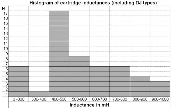
The inductance of the cartridge is a very important element in determining the noise performance, as will shortly be made clear. Figure 9.1 shows the inductance of 51 cartridges, covering both historical and contemporary models. The six types in the “0–300 mH” column are the Grado series. The seven types in the rightmost two columns are DJ types with higher output and inductance than normal hi-fi cartridges; see Chapter 8.
Noise Modelling of RIAA Preamplifiers
The basic noise situation for a series-feedback RIAA stage using an opamp is shown in Figure 9.2. The cartridge is modelled as a resistance Rgen in series with a significant inductance Lgen and is loaded by the standard 47 kΩ resistor Rin; this innocent-looking component causes more mischief than you might think. The amplifier A1 is treated as noiseless, its voltage noise being represented by the voltage generator Vnoise, and the current noise of each input being represented by the current generators Inoise+ and Inoise−, which are uncorrelated. It does not matter to which side of Vnoise the current generator Inoise+ is connected, because Vnoise has no internal resistance and the connections are equivalent. I do not consider 1/f noise and other low- frequency electronic disturbances in detail because there is absolutely nothing you can do about them except choose an appropriately spec’d device or opamp.
Type |
Resistance Ω |
Inductance mH |
|---|---|---|
Audiechnica AT440 |
Not stated |
490 |
Audiechnica AT15SS |
500 |
720 |
CS1 “Carl Cox” |
430 |
400 |
Glanz MFG-31E |
900 |
110 |
Goldring 1006 |
660 |
570 |
Goldring 1012GX |
660 |
570 |
Goldring 1042 |
660 |
570 |
Goldring 2044 |
Not stated |
720 |
Goldring 2100 |
550 |
550 |
Goldring 2200, 2300 |
550 |
680 |
Goldring 2400, 2500 |
550 |
720 |
Goldring Elan |
700 |
560 |
Goldring Elektra |
700 |
560 |
Grado Prestige Green 1, Black 1 |
475 |
45 |
Grado Prestige Red 1, Blue 1 |
475 |
45 |
Grado Reference Sonata 1, Platinum 1 |
475 |
45 |
Ortofon 2M Red, Blue |
Not stated |
700 |
Ortofon 2M Bronze, Black |
Not stated |
630 |
Ortofon OM Super 20 |
1000 |
580 |
Shure ME75-ED Type 2 |
610 |
470 |
Shure ME95-ED |
1500 |
650 |
Shure M97 |
1550 |
700 |
Shure V15V MR |
815 |
330 |
Shure V15V V |
815 |
330 |
Shure V15V IV |
1380 |
500 |
Shure V15V III |
1350 |
500 |
Shure M44G |
650 |
650 |
Stanton 5000 AI |
535 |
400 |
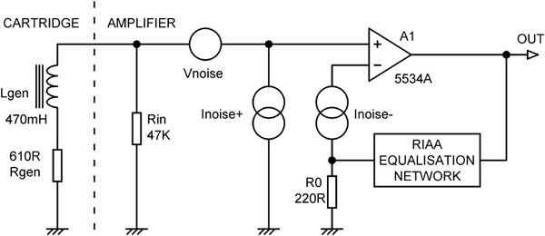
The contributions to the noise at the input of A1 are:
- 1) The Johnson noise of the cartridge resistance Rgen. This sets the ultimate limit to the signal/noise ratio. The proportion of noise from Rgen that reaches the amplifier input falls with frequency as the impedance of Lgen increases. Here the fraction reaching the amplifier falls from 0.99 to 0.48, from 36 Hz to 17.4 kHz. A complication that is not visible in the diagram is that the effective value of Rgen is not simply the resistance of the coils. It increases in value with frequency (while still remaining resistive—we are not talking about inductance here) as a consequence of hysteresis and eddy current magnetic losses in the iron on which the coils are wound, and possibly skin effect.[8] These losses are sometimes modelled by a frequency-dependent resistance placed across Lgen, as by Hallgren,[9] or by a fixed resistance across part of a tapped Lgen.[10] According to Gevel,[11] the losses have little effect on noise issues, and they are not modelled here, not least because of a sad lack of data.
- 2) The Johnson noise of the 47 kΩ input load Rin. Some of the Johnson noise generated by Rin is shunted away from the amplifier input by the cartridge, the amount decreasing with frequency due to the inductance Lgen. Here the fraction reaching the amplifier rises from 0.013 to 0.52, from 36 Hz to 17.4 kHz.
- 3) The opamp voltage noise Vnoise. This contribution is unaffected by other components.
- 4) The noise voltage generated by Inoise+ flowing through the parallel combination of the cartridge impedance and Rin. This impedance increases with frequency due to Lgen. Here it increases from 619 Ω at 36 Hz to 24.5 kΩ at 17.4 kHz; the increase at the top end is moderated by the shunting effect of Rin. This increase has a major effect on the noise behaviour. For the lowest noise you must design for a higher impedance than you might think, and Gevel[11] quotes 12 kΩ as a suitable value for noise optimisation; this assumes A-weighting, inclusion of the IEC amendment, and cartridge parameters of 1000 Ω and 494 mH.
- 5) The Johnson noise of R0. For the values shown, and with A1 assumed to be 5534A, ignoring the Johnson noise of R0 improves the calculated noise performance by only 0.35 dB. The other resistors in the RIAA feedback network are ignored, as R0 has a much lower value, but the RIAA frequency response must of course be modelled. More details of the very limited effect that R0 has on noise performance are given in Chapter 7.
- 6) The noise voltage generated by Inoise− flowing through R0. For normal values of R0, say up to 1000 Ω, this contribution is negligible, affecting the total noise output by less than 0.01 dB.
Contributions 1, 2, and 4 are significantly affected by the rising impedance of the cartridge inductance Lgen with frequency. On top of this complicated frequency-dependent behaviour is overlaid the effect of the RIAA equalisation. This would reduce the level of white noise by 4.2 dB, but we are not dealing with white noise—the HF part of the spectrum has been accentuated by the effects of Lgen, and with the cartridge parameters given, RIAA equalisation actually reduces the noise amplitude by 10.4 dB.
The model as shown does not include the input DC-blocking capacitor Cin. This needs to be 47 uF, or preferably 100uF, so that the voltage produced by the transistor noise current flowing through it is negligible—see Chapter 7.
Clearly this model has some quite complex behaviour. It could be analysed mathematically, using a package such as MathCAD, or it could be simulated by SPICE. The solution I chose is a spreadsheet mathematical model of the cartridge input. The basic method is described by Sherwin.[12] The audio spec- trum is divided into a number of octave bands so RIAA equalisation factors can be applied, and Vnoise, Inoise, and Rgen can be varied with frequency if desired. I extended the Sherwin scheme by using ten octave bands covering 22 Hz to 22 kHz; ten bands are enough to make the process accurate. An advantage of the spreadsheet method is that it is very simple to turn off various noise contributions, so you can experiment with noiseless amplifiers or other flights from physical reality. For example, the noise generated by the 47 kΩ resistor Rin is modelled separately from its loading effects, so they can be switched off independently (see load synthesis later in this chapter). It is also possible to switch off the bottom four octave bands to make the results comparable with real cartridge measurements that require a steep 400 Hz highpass filter to remove the hum. A-weighting can also be switched on and off. The RIAA IEC Amendment can be switched on and off too, but since it only has an effect on very low frequencies the effect on the noise is negligible. The results match well with my 5534, 5532, and TL072 measurements, and experience shows the model is a usable tool. While it is no substitute for careful measurements, it gives a good physical insight and allows noise comparisons at the LF end, where hum is very difficult to exclude completely.
Table 9.2 shows some interesting cases; output noise, EIN, and signal-to-noise ratio for a 5 mV rms input at 1 kHz are calculated for gain of +30.0 dB at 1 kHz. The IEC amendment is included. The cartridge parameters were set to 610 Ω + 470 mH, the measured values for the Shure M75ED 2. Bandwidth is 22 Hz–22 kHz, no A-weighting is used, and 1/f noise is not considered. Be aware that the 5534A is a low-noise version of the 5534, with a typical voltage noise density of 3.5 rather than 4 nV√Hz, and a typical current noise density of 0.4 rather than 0.6 pA/√Hz. There is also an A-version of the 5532, but curiously the data sheets show no noise advantage. The voltage noise and current noise densities used here are the manufacturer’s “typical” figures. I am not aware of any data on how much they vary around the quoted values in practice.

First let us see how quiet the circuit of Figure 9.2 would be if we had miraculously noise-free electronics.
Case 0: We will begin with a completely theoretical situation with no amplifier noise and an MM cartridge with no resistance Rgen. Lgen is 470 mH. Rin is set to 1000 MΩ; the significance of that will be seen shortly. The noise out is a subterranean and completely unrealistic −136.8 dBu, and that is after +30 dB of amplification. This noise comes wholly from Rin and can be reduced without limit if Rin is increased without limit. Thus if Rin is set to 1000 GΩ the noise out is −166.8 dBu.
You may ask why the noise is going up as the resistance goes down, whereas it is usually the other way around. This is because of the high cartridge inductance, which means the Johnson noise of Rin acts as a current rather than a voltage, and this goes up as the Rin resistance goes down.
Case 1: We now switch on the Johnson noise from Rgen (610 Ω). We will continue to completely ignore the cartridge loading requirements and leave Rin at 1000 MΩ, at which value it now has no effect on noise. The output noise with these particular cartridge parameters is then −98.8 dBu (Case 1a). This is the quietest possible condition (if you can come up with a noiseless amplifier), but you will note that right from the start the signal/noise ratio of 85 dB compares badly with the 96 dB of a CD, a situation that merits some thought. And there is, of course, no groove noise on CDs. All of this noise comes from Rgen, the resistive component of the cartridge impedance. The only way to improve on this would be to select a cartridge with a lower Rgen but the same sensitivity, or start pumping liquid nitrogen down the tone arm. (As an aside, if you did cool your cartridge with liquid nitrogen at −196 °C, the Johnson noise from Rgen would only be reduced by 5.8 dB, and if you are using a 5534A in the preamplifier, as in Case 6a below, the overall improvement would only be 0.75 dB. And, of course, the compliant materials would go solid and the cartridge wouldn’t work at all. Hold the cryostats!)
With lower, but still high, values of Rin the noise increases; with Rin set to 10 MΩ (Case 1b) the EIN is −128.7 dBu, a bare 0.1 dB worse. With Rin set to 1 MΩ (Case 1c) the EIN is now −128.2 dBu, 0.8 dB worse than the best possible condition. (Case 1a)
Case 2: It is however a fact of life that MM cartridges need to be properly loaded, and when we set Rin to its correct value of 47 kΩ things deteriorate sharply, the EIN rising by 3.2 dB (compared with Case 1a) to −125.6 dBu. That 47 kΩ resistor is not innocent at all. This case still assumes a noiseless amplifier and appears to be the appropriate noise reference for design, so the noise figure is 0 dB. (However, see the section on load synthesis later in this chapter, which shows how the effects of noise from Rin can be reduced by some non-obvious methods.) Cases 1a,b,c therefore have negative noise figures, but this has little meaning.
Case 3: We leave the amplifier noise switched off but add in the Johnson noise from R0 and the effect of Inoise− to see if the value of 220 Ω is appropriate. The noise only worsens by 0.7 dB, so it looks like R0 is not the first thing to worry about. Its contribution is included in all the cases that follow. The noise figure is now 0.7 dB.
We will now take a deep breath and switch on the amplifier noise.
Case 4: Here we use a single J310 FET, a device often recommended for this application.[11] With the drain current Id set to 10 mA, the voltage noise is about 2 nV√Hz; the current noise is negligible, which is why it is overall slightly quieter than the 2SB737 despite having more voltage noise.
Case 5: In these cases a single discrete bipolar transistor is used as an input device, not a differential pair. This can give superior noise results to an opamp. The transistor may be part of a fully discrete RIAA stage, or the front end to an opamp. If we turn a blind eye to supply difficulties and use the remarkable 2SB737 transistor (with Rb only 2 Ω typical), then some interesting results are possible. We can decide the collector current of the device, so we can to some extent trade off voltage noise against current noise, as described in Chapter 1. We know that current noise is important with an MM input, and so we will start off with quite a low Ic of 200 uA, which gives Case 5c in Table 9.2. The result is very slightly worse than the 5534A (Case 6a). Undiscouraged, we drop Ic to 100 uA (Case 5b), and voltage noise increases but current noise decreases, the net result being that things are now 0.9 dB quieter than the 5534A. If we reduce Ic again to 70 uA (Case 5a), we gain another 0.2 dB, and we have an EIN of −123.6 and a noise figure of only 2.0 dB.
Voltage noise is now increasing fast, and there is virtually nothing to be gained by reducing the collector current further.
We therefore must conclude that even an exceptionally good single discrete BJT with appropriate support circuitry will only gain us a 1.1 dB noise advantage over the 5534A, while the J310 FET gives only a 1.7 dB advantage, and it is questionable if the extra complication is worth it. You are probably wondering why going from a single transistor to an opamp does not introduce a 3 dB noise penalty, because the opamp has a differential input with two transistors. The answer is that the second opamp transistor is connected to the NFB network and sees much more favourable noise conditions; a low and resistive source impedance in the shape of R0.
The 2SB737 is now obsolete. For information on replacements see Chapter 11.
Case 6: Here we have a 5534A as the amplifying element, and using the typical 1 kHz specs for the A-suffix part, we get an EIN of −122.5 dBu and an NF of 3.1 dB. (Case 6a with R0 = 220 Ω) Using thoroughly standard technology, and one of the cheapest opamps about, we are within 3 decibels of perfection; the only downside is that the opportunities for showing off some virtuoso circuit design with discrete transistors appear limited. Case 6a is useful as a standard for comparison with other cases, as in the rightmost column of Table 9.2.
First, how does the value of R0 affect noise? In Case 6b R0 is increased to 470 Ω, and the noise is only 0.4 dB worse; if you can live with that, the increase in the impedance of the RIAA feedback network allows significant savings in expensive precision capacitors. Reducing R0 from 220 Ω to 100 Ω is doable at some cost in capacitors but only reduces the noise output by 0.2 dBu. In Chapter 7 the value of R0 can be manipulated to get convenient capacitor values in the RIAA network, because it has only a weak effect on the noise performance.
Second, we have seen that the presence of Lgen has a big effect on the noise contributions. In Case 6a, if we reduce Lgen to zero the noise out drops from −92.5 to −94.7 dBu. Halving it gives −93.8 dBu. Minimum cartridge inductance is a good thing.
Third, what about Rgen? With the original value of Lgen, setting Rgen to zero only reduces the noise from −92.5 to −93.5 dBu; the cartridge inductance has more effect than its resistance.
Case 7: The OPA1642 is a relatively new JFET input opamp with noise densities of 5.1 nV/√Hz for voltage and a startlingly low 0.0008 pA/√Hz for current. This modern JFET technology gives another way to get low MM noise—accept a higher en in order to get a very low in. The OPA1642 gives an EIN of −121.8 dBu, beating the 5532 but not the 5534A with R0 = 220 Ω. At the time of writing the OPA1642 is something like 20 times more expensive than the 5532.
Case 8: We go back to the 5534A, with R0 now raised substantially further to 1000 Ω, and the noise is now 1.1 dB worse than the 5534A 220 Ω case. This is a good demonstration that the value of R0 is not critical.
Case 9: It is well-known that the single 5534A has somewhat better noise specs than the dual 5532A, with both en and in being significantly lower, but does this translate into a significant noise advantage in the RIAA application? Case 7 shows that on plugging in a 5532A the noise output increases by 2.0 dB, the EIN increasing to −120.5 dBu. The NF is now 5.1 dB, which looks a bit less satisfactory. If you want good performance, then the inconvenience of a single package and an external compensation capacitor are well worth putting up with. If your circuit design ends up with an odd number of half-5532s per channel, a 5534A can be placed in the MM stage, where its lower noise is best used.
Case 10: Here we try out the FET-input OPA2134, which is a good opamp when DC accuracy and low bias currents are required; we find the en is much higher at 8 nV√Hz, but in is very low indeed at 3 fA√Hz. It looks like we might be in with a chance, but the greater voltage noise does more harm than the lower current noise does good, and the EIN goes up to −119.3 dBu. The OPA2134 is therefore 3.2 dB noisier than the 5534A and 2.5 dB noisier than the 5532A; and it is not cheap. The noise figure is now 6.3 dB, which to a practised eye would show that something had gone amiss in the design process.
Case 11: The LM4562 BJT input opamp gives significant noise improvements over the 5534/5532 when used in low-impedance circuitry, because its en is lower at 2.7 nV√Hz. However, the impedances we are dealing with here are not low, and the in, at 1.6 pA√Hz, is four times that of the 5534A, leading us to think it will not do well here. We are sadly correct, with EIN deteriorating to −117.9 dBu and the noise figure an unimpressive 7.7 dB. The LM4562 is almost 5 dB noisier than the 5534A and at the time of writing is a lot more expensive. Measurements confirm a 5 dB disadvantage.
Case 12: The LME49720 is a recent BJT input opamp with the same voltage and current densities as the LM4562, and so gives the same EIN of −117.9 dBu, 5 dB noisier than the 5534A.
Case 13: The OPA604 is a FET-input opamp that is often recommended for MM applications by those who have not studied the subject very deeply. It has noise densities of 10 nV/√Hz for voltage and a low 0.004 pA/√Hz for current. This different balance of voltage and current noise results again in the same EIN of 117.9 dBu, 5 dB noisier than the 5534A.
Case 14: The OP275 has both BJT- and FET-input devices. Regrettably this appears to give both high voltage noise and high current noise, resulting in a discouraging EIN of −117.3 dBu and a noise figure of 8.2 dB. It is 5.2 dB noisier than a 5534A in the same circuit conditions. Ad material claims “excellent sonic characteristics”, perhaps in an attempt to divert attention from the noise. It is expensive.
Case 15: The AD797 has very low voltage noise because of its large BJT input transistors, but current noise is correspondingly high, and it is noisy when used with an MM cartridge. And it is expensive, especially so since it is a single opamp with no dual version. Definitely not recommended for MM; allegedly useful in submarines.
Case 16: The TL072 with its FET-input has very high voltage noise at 18 nV√Hz but low current noise. We can expect a poor performance. We duly get it, with EIN rising to −113.4 dBu and a very indifferent noise figure of 12.2 dB. The TL072 is 9.1 dB noisier than a 5534A and 8.4 dB noisier than a 5532A. The latter figure is confirmed (within experimental error, anyway) by the data listed in the later section on noise measurements. There is now no reason to use a TL072 in an MM preamp; it must be one of the worst you could pick.
Case 17: Just for historical interest I tried out the LM741. The voltage noise measures about 20 nV√Hz. I have no figures for the current noise, but I think it’s safe to assume it won’t be better than a 5532, so I have used 0.7 pA√Hz. Predictably the noise is the highest yet, with an EIN of −112.4 dBu, but it is a matter for some thought that despite using a really ancient part it is only 10 dB worse than the 5534A. The noise figure is 13 dB.
Opamps with Bias Cancellation
You may be wondering what has happened to other well-known opamps, particularly the OP-27 and the LT1028. Both are sometimes recommended for audio use because of their low voltage noise density (en), but this ignores a serious problem. The OP-27 has a low en of 3 nV/√Hz and in of 0.4 pA/√Hz and from these figures alone gives a calculated EIN of −123.0 dB, which beats the 5532A noise, but … when you measure it in real life it is actually several dB noisier; I have confirmed this several times. This is due to extra noise generated by bias- current cancellation circuitry. Correlated noise currents are fed into both inputs and will only cancel if both inputs see the same impedance. In this MM RIAA application the impedances are wildly different, and the result is much increased noise. This problem with the OP-27 was originally pointed out to me by Marcel van de Gevel.[13]
The LT1028 gives a poor performance in MM applications because, while it has an appealingly low en of 0.85 nV√Hz, its in is high at 1 pA√Hz as a result of running big input BJTs at high collector currents. The EIN is by calculation −120.9 dBu, making it a shade quieter than the 5532A. But … the LT1028 also has bias-current cancellation circuitry, and the data sheet explicitly states: “The cancellation circuitry injects two correlated current noise components into the two inputs.” According to Gevel,[11] the effective voltage noise in a typical MM application is about 39 nV/√Hz, so even the LM741 would be a better choice.
A relatively new addition to this group is the OP2227, which has promising noise densities of 3 nV/√Hz for voltage and 0.4 pA/√Hz for current, the same as the OP27, which figures give the same calculated EIN of −123.0 dB. It has however bias-current cancellation, and while I have no practical experience with this opamp, there seems no reason why it should not have the same excess noise problem as the OP27 and LT1028.
Hybrid Phono Amplifiers
In Table 9.2 the noise results are shown for single discrete devices as well as opamps. These cannot of course be used alone in a phono amplifier because of the need for both substantial open-loop gain and good load-driving ability. The discrete device can be used as the first stage of a discrete amplifier, as described in Chapter 10, but it is more convenient to combine the discrete device with an opamp, which will give both the open-loop gain and the load-driving ability required at lower cost and using less PCB area. The 5532 or 5534 is once again very suitable.
Figure 9.3 shows a basic arrangement. For optimal noise the Ic of Q1 will probably be in the range 50–200 uA, and most of this is supplied through R8. While there is always a DC path through the RIAA network because of the need to define the LF gain, trying to put all of the Ic through it would lead to an excessive voltage drop, which would appear as a big offset at the output. Instead the DC flowing through R1 is just used for fine tuning of Q1 operating conditions by negative feedback. This means that if R8 and Vbias are correctly chosen, there might be a few 100mV of offset either way at the opamp output. This is not large enough to significantly affect the output swing, but it needs blocking; C5 is shown as nonpolar to emphasise the point that the offset might go either way.
C7 gives dominant-pole compensation of the loop; the RIAA usually causes the closed-loop gain to fall to unity at high frequencies (but see the section on switched-gain phono amps in Chapter 7), and achieving HF stability may require some experimentation with its value. The two supply rails are heavily filtered by R6, C5 and R7, C6 to keep out ripple and noise; no fancy low-noise supply is needed, 78/79 series regulators work just fine.
A more sophisticated hybrid amplifier is demonstrated by the MC amplifier in Chapter 11, where R0 is 3.3 Ω and C0 would be inconveniently large at 4700 uF. To avoid this the negative feedback network has the same gain at DC as AC, and the standing output voltage is controlled by a DC servo.
Noise in Balanced MM Inputs
So far all the MM amplifiers considered have been of the usual unbalanced input type. There is a reason for this.
There is some enthusiasm out there for balanced MM inputs, on a “me-too!” basis, because they are almost universally used in professional audio for excellent reasons. However, an MM cartridge and its short connecting lead (short to control shunt capacitance) are nothing like the average professional connection that links two pieces of powered equipment and so is likely to have nasty currents flowing through its ground wire. The internals of an MM cartridge are shown in Figure 6.1; the coils are floating. How might common-mode interference, which is what balanced inputs reject, get into the cartridge or lead?

- 1) Electrical fields into the cartridge. Any sensible cartridge is electrically shielded, so balancing is not required. For electrically unscreened cartridges (there is one brand that is globally famous for humming), the coupling will not be identical for the two ends of the coil, so it won’t be a true common-mode signal; I dare say you could have a “balanced” input in which you set the gain of hot and cold inputs separately so you could try to null the hum. Good luck getting that to stay nulled as the arm moves across the disc; this not an idea to pursue.
- 2) Magnetic fields into the cartridge. These will cause a differential voltage across the floating cart coil, just as for the signal, and will not be rejected in any way by a balanced input.
- 3) Electrical or magnetic coupling into the cable. Negligible with usual cable lengths and even half-sensible cable layout; i.e. keep it away from mains wiring and transformers. A balanced input is therefore not required.
These points were debated at length on DIYaudio, and no evidence was offered that they were wrong. For this reason balanced MM inputs receive only limited attention in this book.
When dealing with line inputs, a balanced input is much noisier than an unbalanced input. The conditions for an MM balanced input are quite different, but it still seems highly likely that it will be noisier because two (or more) amplifiers are used rather than one, and we don’t want a noise penalty if there are no countervailing benefits. Let’s find out …
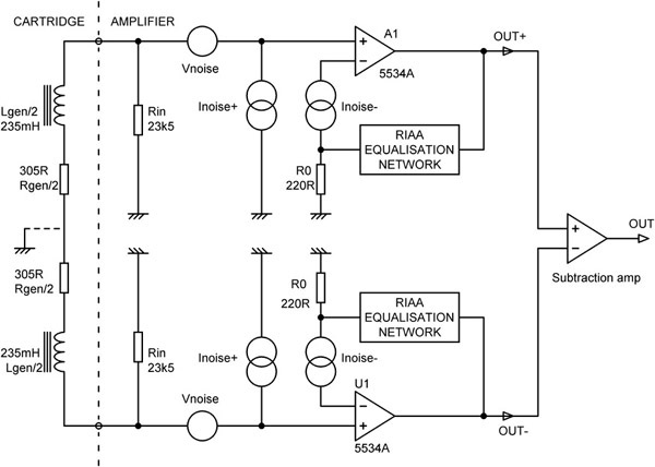
Figure 9.4 depicts a balanced MM input made up of two 5534A stages with their outputs subtracted (or “phase-summed”). All the noise sources are shown. The equal loading on each cartridge pin makes the coil appear balanced to the amplifiers; the “ground” at the midpoint of the cartridge is purely notional, with no physical connection there.
Therefore the 47 kΩ load is split into two 23.5 kΩ resistances; these give less Johnson noise by a factor of √2, and also the voltage produced by Inoise+ will be halved. The Vnoise is unaffected, and we now have two uncorrelated sources of it.
The unweighted noise output for a standard unbalanced 5534A amplifier in a +30 dB (1 kHz) amplifier is −92.51 dBu, as in Table 9.2. Cartridge parameters are 610 Ω + 470 mH. Reducing Rin to 23.5 kΩ and changing the cartridge parameters to 305 Ω + 235 mH, as we are only dealing with half of the cartridge, reduces the noise output to −94.36 dBu. We then have to subtract the outputs of the two sides, which is equivalent to summing their noise. Neglecting the noise of the subtracting amplifier, which is quite realistic given the relatively high noise output of the input stages, the result is −91.36 dBu. This is only 1.1 dB noisier than an unbalanced input, and would be quite acceptable if a balanced input solved other problems, but as noted earlier I’ve yet to hear any convincing argument that it does.
The arrangement of Figure 9.4 is an illustration of principle and is not claimed to be optimal. For one thing, there are two RIAA networks, and they are very likely the most expensive part of the circuit. They will have to be accurate for accurate RIAA, and that may well be enough to give a good practical CMRR, if you can find a use for it.
Figure 9.4 uses two opamps, which effectively puts four input devices in series in the input circuit, though the two on the opamp inverting inputs see benign noise conditions in the shape of the low resistance of R0. This could be addressed by using an instrumentation amplifier IC, but the possible noise advantage is small.
Noise Weighting
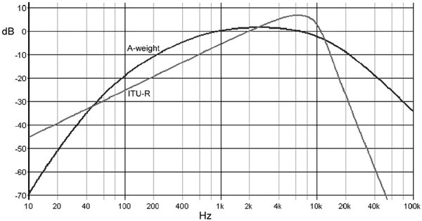
The frequency response of human hearing is not flat, especially at lower listening levels. Some commentators therefore feel it is appropriate to use psychoacoustic weighting when studying noise levels. This is almost invariably ANSI A-weighting despite the fact that it is generally considered inaccurate, as it undervalues low frequencies. ANSI B-, C-, and D-weightings also exist but are not used in audio. The ITU-R ARM 468 weighting (CCIR-468) is a later development and generally considered to be much better but is only rarely used in audio (ARM stands for Average-Responding Meter). I prefer unweighted measurements, as you are one step closer to the original data.
A-Weighting
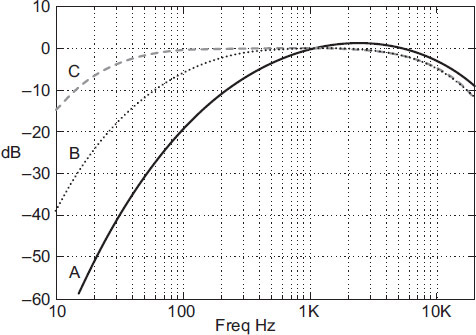
The A-weighting curve is shown in Figure 9.5. It approximately follows the Fletcher-Munson 40-phon line. It passes through 0 dB at 1 kHz and has a maximum gain of 1.3 dB at 2.5 kHz. The low-frequency roll-off steadily steepens as frequency falls, while the high-frequency roll-off is at 12 dB/octave (−3 dB at 12 kHz).
A-weighting is defined in the ANSI S1.42 standard. The required filter design is based on direct implementation of the filter’s transfer function based on poles and zeros; no standard circuit is given. The EU version of the standard is IEC 61672–1, which does not even give the poles and zeros; it simply requires that the filter magnitudes fall within a specified error mask. This accounts for the extraordinarily wide variation in circuitry that appears if you do an image search on Google for “A-weighting schematics”. Their accuracy is a matter for speculation, so I present my version in Figure 9.6; awkward component values abound, here implemented as 2xE24 resistors and E12-series capacitors. E6 capacitors could be used, but it would mean a lot more paralleling to get suitably accurate values. The filter is accurate to the A-weighting spec within ±0.1 dB over 80 Hz–20 kHz. Below 80 Hz the error slowly grows to 0.5 dB, but since this is at filter attenuations of more than 20 dB the effect on measurements will be negligible.
The wholly passive weighting network has a loss at 1 kHz of −18.37 dB, and the A1 stage simply brings the overall gain at this frequency back up to 0 dB. It is assumed that the noise being measured has already been brought up to a suitable level (say 0 dBu) and so is immune to contamination by any normal opamp circuit noise.
A-weighting reduces the level of white noise by 4.4 dB, but as noted earlier we are not dealing with white noise here, as the spectrum is altered by the effects of the cartridge Lgen and the RIAA equalisation. Useful information on this and the effects of A-weighting on the result are given by Hallgren.[9]
You may therefore be wondering how the unweighted results described earlier will be affected by the application of A-weighting. Will the order of merit in Table 9.2 be upset?
Table 9.3 shows the effects of A-weighting on selected cases from Table 9.2. The noise level drops by between 2 and 4 dB, depending on the magnitude of voltage noise compared to current noise. A-weighting does not introduce any revolutionary changes into the order of merit of the various amplifiers in Table 9.2.
Case |
Amplifier type |
Unweighted noise out dBu |
A-weighted noise out dBu |
A-weighting difference dB |
|---|---|---|---|---|
5a |
2SB737 70uA |
−93.6 |
−96.3 |
2.7 |
5b |
2SB737 100uA |
−93.4 |
v96.0 |
2.6 |
5c |
2SB737 200uA |
−92.7 |
−95.1 |
2.4 |
6a |
5534A |
−92.5 |
−95.4 |
2.9 |
7 |
5532A |
−90.5 |
−93.3 |
2.8 |
8 |
OPA2134 |
−89.3 |
−92.8 |
3.5 |
9 |
LM4562 |
−87.9 |
−89.9 |
2.0 |
11 |
TL072 |
−83.4 |
−87.1 |
3.7 |
ITU-R Weighting
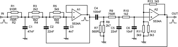
The ITU-R ARM weighting is compared with A-weighting in Figure 9.7. The specification for the ITU-R ARM 468 weighting differs in that the circuit of a standard passive filter is given; unfortunately this requires two unwelcome inductors, and every value is awkward. Not even the 600 Ω terminating resistor can be found in the E96 series. It is therefore more commonly implemented as an active filter. The LF side of the ITU curve has a 6 dB/octave slope, while the HF roll-off has a much steeper 30 dB/octave slope, indicating that a 5th-order lowpass filter is required. The ITU-R is normally implemented to give 0 dB at 2 kHz rather than 1 kHz, as this reduces the amount of gain around 5 kHz and reduces the likelihood of headroom problems. My version is shown in Figure 9.8. This is accurate to within ±0.1 dB over 10 Hz–31 kHz.
In Figure 9.8 the 5th-order lowpass is composed of the 3rd-order lowpass stage using A1, which has no gain peaking above 0dB and no internal headroom issues, and the 2nd-order lowpass stage around A2, whose gain is chosen to give the desired Q. The 6dB/octave LF roll-off is implemented by C4 and R7, R8. A low-impedance drive is required to the input, as with all the filters described in this book.
RIAA Noise Measurements
In the past, many people who should have known better have recommended that MM input noise should be measured with a 1 kΩ load, presumably thinking that this emulates the resistance Rgen, which is the only parameter in the cartridge actually generating noise—the inductance is of course noiseless. This overlooks the massive effect that the inductance has in making the impedance seen at the preamp input rise very strongly with frequency, so that at higher frequencies most of the input noise actually comes from the 47 kΩ loading resistance. I am grateful to Marcel van de Gevel for drawing my attention to some of the deeper implications of this point.[13]
The importance of using a real cartridge load is demonstrated in Table 9.4, where the noise performance of a TL072 and a 5532 are compared. The TL072 result is 0.8 dB too low, and 5532 result 4.9 dB too low—a hefty error. In general results with the 1 kΩ resistor will always be too low, by a variable amount. In this case you still get the right overall answer—i.e. you should use a 5532 for least noise—but the dB difference between the two has been exaggerated by almost a factor of two by undervaluing the 5532 current noise.
These tests were done with an amplifier gain of +29.55 dB at 1 kHz. Bandwidth was 400 Hz–22 kHz to remove hum, rms sensing, no weighting, cartridge parameters were 610 Ω + 470 mH.
Zsource |
TL072 |
5532 |
5532 benefit |
5532 EIN |
|---|---|---|---|---|
1 kΩ resistor |
−88.0 |
−97.2 dBu |
+9.8 dB |
−126.7 dBu |
Shure M75ED 2 |
−87.2 |
−92.3 dBu |
+5.1 dB |
−121.8 dBu |
The 1 kΩ recommendation was perhaps made because the obvious measurement method of loading the input with a MM cartridge has serious difficulties with hum from the ambient magnetic fields. To get useful results it is essential to enclose the cartridge completely in a grounded mumetal can—I use a can from a redundant microphone transformer, and it works very well. I suppose the ideal load would be a toroidal inductor, but it would be an expensive custom part. It is also necessary to use complete electrostatic screening of the amplifier itself. If it has a 22 uF input coupling capacitor and the input is short-circuited, the impedance downstream of the capacitor is 145 Ω at 50 Hz, which is enough to make it susceptible to electrostatic hum pickup.
RIAA Amps Driven from an MC Head Amp
All the discussion above deals with an RIAA preamplifier driven by an MM cartridge. As we noted at the start, the MM RIAA stage may also be driven from an MC head amp. The noise conditions for the RIAA amplifier are quite different, as it is now fed from a very low impedance, plus probably a series resistor in series with the MC amp output to give stability against stray capacitances. My current MC head amp design (see Chapter 12) has an EIN of −141.5 dBu with a 3.3 Ω input source resistance. Its gain is +30 dB, so the output noise is −111.5 dBu. The series output resistor is 47 Ω; its Johnson noise at −135 dBu is negligible, and likewise the effect of the RIAA stage input current noise flowing in it. The noise at the output of the RIAA stage is then −85.7 dBu, which is higher than any of the figures in Table 9.2 except those for TL072 and LM741. In this situation the value of R0 is relatively unimportant.
Cartridge Load Synthesis for Lower Noise
Going back to Table 9.2, you will recall that when we were examining the situation with the amplifier and feedback network noise switched off, adding in the Johnson noise from the 47 kΩ loading resistor Rin caused the output noise to rise by 3.2 dB. In real conditions with amplifier noise included the effect is obviously less dramatic, but it is still significant. For the 5534A (Case 6a) the removal of the noise from Rin (but not the loading effect of Rin) reduces the noise output by 1.3 dB. Table 9.5 summarises the results for various amplifier options; the amplifier noise is unaffected, so the noisier the technology used, the less the improvement.
This may appear to be utterly academic, because the cartridge must be loaded with 47 kΩ to get the correct response. This is true, but it does not have to be loaded with a physical 47 kΩ resistor. An electronic circuit that has the V/I characteristics of a 47 kΩ resistor, but lower noise, will do the job very well. Such a circuit may seem like a tall order—it will after all be connected at the very input, where noise is critical, but unusually, the task is not as difficult as it seems.
Figure 9.9a shows the basic principle. The 47 kΩ Rin is replaced with a 1 MΩ resistor whose bottom end is driven with a voltage that is phase-inverted and 20.27 times that at the top end. If we conceptually split the 1 MΩ resistor into two parts of 47 kΩ and 953 kΩ, a little light mathematics shows that with −20.27 times Vin at the output of A2, the voltage at the 47 kΩ–953 kΩ junction A is zero, and so as far as the cartridge is concerned it is looking at a 47 kΩ resistance to ground. However, the physical component is 1 MΩ, and the Johnson current noise it produces is less than that from a 47 kΩ (Johnson current noise is just the usual Johnson voltage noise applied through the resistance in question). The point here is that the apparent resistor value has increased by 21.27 times, but the Johnson noise has only increased by 4.61 times because of the square root in the Johnson equation; thus the current noise injected by Rin is also reduced by 4.61 times. The noise reduction gained with a 5534A (Case 6a) is 1.3 dB, which is very close to the 1.5 dB improvement obtained by switching off the Rin noise completely. If a resistor larger than 1 MΩ is used slightly more noise reduction can be obtained, but that would need more gain in A2, and we would soon reach the point where it would clip before A1, restricting headroom. In this case, with a gain of 21 times, we get a very good noise figure of 1.8 dB, though the lowest noise output comes from the 2SB737 at 70 uA.

The implementation made known by Gevel[11] is shown in Figure 9.9b. This ingenious circuit uses the current flowing through the feedback resistor R0 to drive the A2 shunt-feedback stage. With suitable scaling of R3 (note that here it has an E96 value), the output voltage of A2 is at the right level and correctly phase-inverted. When I first saw this circuit I had reservations about connecting R0 to a virtual ground rather than a real one and thought that extra noise from A2 might find its way back up R0 into the main path. (I hasten to add that these fears may be quite unjustified, and I have not found time so far to put them to a practical test.) The inverting signal given by this circuit is amplified by 20.5 times rather than 20.27, but this has a negligible effect on the amount of noise reduction.

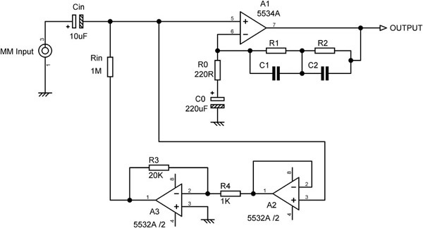
Because of these reservations, I tried out my version of load synthesis as shown in Figure 9.10. This uses the basic circuit of Figure 9.9a; it is important that the inverting stage A3 does not load the input with its 1 kΩ input resistor R4, so a unity-gain buffer A2 is added. The inverting signal is amplified by 20 times, not 20.27, but once again this has negligible effect on the noise reduction.
In practical measurements with a 5534A as amplifier A1, I found that the noise improvement with a real cartridge load (Shure M75ED 2, cartridge parameters 610 Ω + 470 mH) was indeed 1.3 dB, just as predicted, which is as nice a matching of theory and reality as you are likely to encounter in this world. There were no HF stability problems. Whether the 1.3 dB is worth the extra electronics is a good question; I say it’s worth having.
When measuring the effect of load synthesis, it is highly convenient to be able to switch immediately between normal and synthesised modes. This can be done with one link, as shown in Figure 9.11, which uses the basic circuit of Figure 9.10. Adding link J1 loads the input with the physical 47 kΩ resistor Rin1, and at the same time short-circuits the output of A3 to ground. The 953 kΩ resistor Rin2 is made up of two E24 resistors in parallel, which give a combined value only 0.26% below the nominal value.
This technique has been called “electronic cooling”, presumably because it could be regarded as analogous to dipping the loading resistance in liquid nitrogen or whatever to reduce Johnson noise. I must admit I don’t like the term, as it could be understood to mean that thermoelectric elements have been used to cool down the input stage, a technique I do not think has been used in hi-fi yet. I prefer to call it “electronic loading”, “active input impedance”, or “load synthesis”, the last being perhaps the most explicit. It would also be useful for tape head preamplifiers, but they are a bit of a minority interest these days.

The History of Load Synthesis
Yet again we encounter a technique that has a longer history than you might expect. The first appearance of it that is known to me is a paper by W. S. Percival called an “An Electrically ‘Cold’ Resistance”.[14] He used a transformer between the anode and grid of a valve amplifier for the voltage scaling and phase inversion and thus emulated a resistance having an effective temperature of only 70° K. Thus the idea of describing it as “electronic cooling” has been with us from the start.
The same technique was later expanded upon by Strutt and Van der Ziel.[15] It was also briefly summarised by Van der Ziel in his treatise “Noise”.[16]
Load synthesis was referred to by Tomlinson Holman in his famous 1975 paper “New Factors In Phonograph Preamplifier Design”[17] (which is still well worth reading) as a recent innovation:
Two noise reduction techniques have appeared in recent designs. One is to use quite low impedances in the RIAA feedback … The second involves the use of a synthesized input impedance through the use of an extra feedback loop which bootstraps the cartridge termination resistor to reduce its noise contribution. One commercial embodiment of the bootstrap method produced a signal-to-noise ratio of 85 dB re 10 mV, 1 kHz input, ANSI ‘A’ weighted with a cartridge input.
For comparison, assuming the reference level is 10 mV rms, the 5534A in Case 6a gives an unweighted S/N ratio of 84.7 dB without load synthesis and 86.0 dB with it. Clearly it has a better noise performance than whatever was used in the “commercial embodiment”.
Bootstrapping is not really the right term; load synthesis is more “anti-bootstrapping” in that it makes a large impedance look like a small one by applying a voltage in anti-phase, whereas conventional bootstrapping makes a small impedance look like a large one by applying a voltage in phase. I have no idea which “commercial embodiment” he was talking about, and I would be very glad to hear any suggestions. So far I have had none, and I’m sure you all can do better than that.
The technique was analysed by Hoeffelman and Meys in the JAES in 1978.[18] The only relevant patents found so far are US 4 156 859 granted to Robert L. Forward in October 1977, which describes the use of opamps and transformers for voltage scaling and phase inversion, and US 4 232 280 (same guy), which uses FET source-followers instead of opamps.
Noise Gating
We saw earlier in this chapter that there are definite physical limits to how low the noise of a preamplifier driven by an MM cartridge can be. Noise in the quiescent state is particularly noticeable when headphones are in use. So if you want less noise, there is nothing to be done? Ha! In electronics there is almost always something that can be done.
First it has to be recognised that cartridge and preamplifier noise is pretty much irrelevant while a disc is playing. Groove noise will be something like 30 dB higher. So to make an audible difference the only thing to do is reduce the noise when a disc is not playing. This can be done most effectively by the use of a noise gate, which cuts the signal completely when it falls below a certain threshold. You probably think this is a dreadful idea, and under most circumstances it would be, with the noise gate chopping in and out in quiet passages of music. But … the difference between vinyl and all other sources is that it carries subsonic disturbances that are always present, even if the audio signal disappears completely. Even disc pressings of the highest quality produce this subsonic information, at a surprisingly high level, partly due to the RIAA bass boosting. The subsonic component is often less than 20 dB below the total programme level, and this is more than sufficient to keep the gate open (unmuted) for the duration of an LP side. (See Chapter 12.) Therefore all that is required is a noise gate with a response down to around 1 Hz.
The noise gate will have the usual fast-attack, slow- decay characteristic, so the preamplifier is unmuted as soon as the stylus touches the disc, and muted about a second after it has been raised from the run-out groove. This delay can be made short because the relative quiet at the start of the run-out groove is sensed and stored. The rumble performance of the record deck is largely irrelevant because virtually all of the subsonic information is generated by disc irregularities.
A noise gate is composed of a high-gain amplifier to bring low-level signals up to a convenient level, a peak rectifier with fast attack and slow decay, a comparator that switches at a set threshold; this is called the side-chain because signal does not go through it and come out the other end. The comparator controls a muting element. It is often convenient to use the mute relay, which prevents switch-on thumps. The signal pick-off point must clearly be before any subsonic filtering and ideally where the signal has reached its full nominal level. If this is not possible because the subsonic filtering is done at a lower level, then more gain must be built into the side-chain to compensate.
Figure 9.12 shows an early noise gate design that was used in the Advanced Preamplifier of 1976.[19] It worked flawlessly at the time (and indeed it still does) so is worth a look.
The side-chain begins with two amplifiers with gains of 101 times, one for each channel. The inputs are clamped with diodes so that main signal path can use its full voltage swing capability without damaging the opamps. You will note they are shown as the 741 types used at the time. They are elderly but more than adequate for the task here, so this is a good place to use up some vintage parts. They are powered from the +24V and 0V rails. Fed with the nominal signal voltage of 800 mV rms (+0.3 dBu), the opamp outputs move continuously between positive and negative clipping due to the high gain; this keeps the peak-rectifier capacitor C3 fully charged. In the silent-ish passages between LP tracks the subsonic signal is not normally of sufficient amplitude to cause them to clip but will usually produce at least +3 to +4 V across C3, which gives a large margin of safety against unwanted muting.
When the stylus is lowered onto a record, C3 charges rapidly through D3, and when its voltage exceeds the +0.6V reference set up by R5–D5, the output of A2 goes high, switching on Q2, energising the mute relay, and letting signals through to the preamplifier output. This happens very quickly, and you are never going to miss the first note of the music, so long as you put the needle down in the right place.
When the stylus leaves the record surface and the subsonic signals cease, C3 slowly discharges through R4 until A2 output goes low, cutting off the base drive to Q2, and so switches off the relay.
The threshold for unmuting is determined from the gain of A1 and the +0.6V reference; a level of 850 mV rms at A1 output (allowing for the diode forward drop of D3) will switch A2, corresponding to an input level of 8.5 mV rms (equal to −39 dBu). As shown, the noise gate monitors both stereo channels and selects the maximum with D3, D4, but on reflection (and I’ve had 40 years to think it over) monitoring just one channel should work equally well, even if it has a vaguely unsettling feeling of asymmetry about it; a useful number of parts are saved. What you should NOT do is monitor the sum of the two channels, as much of the subsonic information is in anti-phase and will tend to cancel.
The noise gate will only work properly with vinyl inputs, so it is disabled when any other input is selected. An extra wafer on the source-select switch SW1 is arranged to provide permanent unmute when required by pulling the inverting input of A2 low so the output of A2 will stay high even when there is no signal and C3 is fully discharged. Q1 is part of the switch-on delay system—at power-up Q1 was turned on to prevent Q2 switching on; there is a bit of a trap here because it is essential to get Q1 turned on fast before the relay has time to close. The original circuit worked reliably, but it would be much safer to rearrange things so that the switch-on delay supplies an enable rather than a disable for the relay circuit. This will be essential if a microcontroller is providing the switch-on delay, as they take a little time to initialise themselves when the power is applied.

One rough edge of this design is the side-chain amplifier, which spends most of its time clipping hard. The currents drawn from the supplies and put into the ground have sharp edges, and the connections must be arranged to keep them out of the audio supplies and ground. There are also large square-wave-ish voltages on the opamp outputs which must not be allowed to couple capacitively into the audio path.
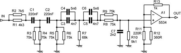
There are more sophisticated ways to deal with these problems. Figure 9.13 shows a side-chain designed originally for a signal activation system to bring a power amplifier out of standby when a signal appeared at the input; it has been adapted for use as a subsonics- activated noise gate by extending the LF response. The first amplifier stage U1:A has a mid-band gain of +38 dB and uses shunt feedback in the usual way to generate a virtual-earth at Pin 2. The feedback network R2, R3, R4 is in the form of a T-network to give high gain without excessively high resistor values. C2 across R2 provides an HF roll-off of −3 dB at 16 kHz to discriminate against HF noise. C3 reduces the gain to unity at DC to minimise offset voltages and gives an LF roll-off at 0.5 Hz. D1 and D2 are 2V4 Zener diodes that provide output clamping by increasing the negative feedback when the output exceeds about 3V peak in either direction; the opamp is always under feedback control and so does not generate sharp edges by clipping.
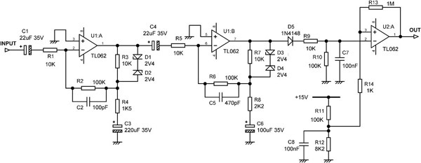
The second amplifier stage, U1:B, is a similar shunt-feedback stage with a virtual-earth at Pin 2 and a mid-band gain of +35 dB. It is fed from the first stage via capacitor C4 and input resistor R5, which create a roll-off −3 dB at 0.7 Hz. R8 and C6 give an LF roll-off of −3 dB at 0.7 Hz, while R6 and C5 give an HF roll-off −3 dB at 3.4 kHz to prevent false triggering from noise pulses. D3 and D4 are 2V4 Zener diodes that provide output clamping.
D5 and C7 are the peak rectifier, with a slow attack time set by R9 (to further discriminate against noise pulses) and the decay time set by R10. The stored voltage on C7 is applied to comparator U2:A; R13 and R14 provide a small amount of positive feedback to introduce a touch of hysteresis and so give clean comparator switching. TL062 opamps, rather than the more familiar TL072, are used because of their lower input offset voltage.
The comparator reference of +1.2 V is set by the divider R11, R12. Allowing for a 0.6 V forward drop in D5, a peak voltage of 1.8V is therefore required at the output of U1:B to trip the comparator, equivalent to +4.3 dBu. This is given by 4.3 − (38 + 35) = −68.7 dBu, which is 284 uV. This is a much lower trip level than the first design in Figure 9.12 (which is −39 dBu) because it is intended to derive its input from before any subsonic filtering. I have recommended that a phono input stage should not have a greater gain than +30 dB at 1 kHz if a really good overload margin is desired, and so the nominal output for 5 mV rms in is only 158 mV rms, (both at 1 kHz) which is −13.8 dBu. Therefore more amplification is required and two stages are used. The difference between the nominal output and the noise gate trip point is 40 dB for the original design and 55 dB for the later design, and both have worked reliably for many years.
If lower sensitivity is required for the circuitry of Figure 9.13, the gain of either or both amplifier stages can be reduced. If higher sensitivity is sought then the best way is to leave the amplifiers alone and instead reduce the reference voltage set by R11, R12. I have tested it down to +260 mV from +1.2 V, increasing the sensitivity by another 13 dB. Beyond this you are on your own, and care will be required in layout and grounding to prevent positive feedback and false triggering. This circuitry was used in a large number of amplifiers, starting about 14 years ago; it is still in production at the time of writing.
Before we leave this subject, I would like to emphasise that foolproof noise gating which never cuts off a wanted signal is feasible only for a vinyl signal, with its inevitable background of subsonic disturbances. It will not work so well with line sources that do not have a subsonic accompaniment.
Distortion in MM RIAA Amplifiers
An RIAA stage with a gain of +30 dB at 1 kHz will have a gain of about +50 dB at 20 Hz; that is high for a single-opamp stage. The closed-loop gain at HF is about +10 dB, so the feedback factor can be maintained there without problems; fortunately, the RIAA curve roughly follows the 6 dB/octave fall in open-loop gain. The CM voltage is very small and should not cause distortion.
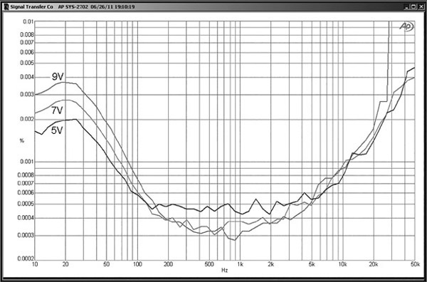
Figure 9.14 shows the distortion of a 5534A +30 dB RIAA stage at 5 V, 7 V, and 9 Vrms out. The distortion at LF is mainly second harmonic; it was checked that this was not coming from C0; increasing it from 220uF to 1000/6V3 gave no improvement. It must be coming from the opamp. The sudden increase in distortion at about 27 kHz for the 9 Vrms case occurs when the current drawn by the RIAA network reaches the limits of the output capability of the 5534A. Note that 9 Vrms is a whole 36 dB above the nominal operating level of 150 mV rms out.
The distortion will be aggravated by external loading. Here we have just the HF correction pole, which only places an extra load on the opamp at HF. If it is removed, the distortion at low and middle frequencies is completely unchanged, but the sudden increase in distortion for the 9 Vrms case now occurs at the higher frequency of 36 kHz.
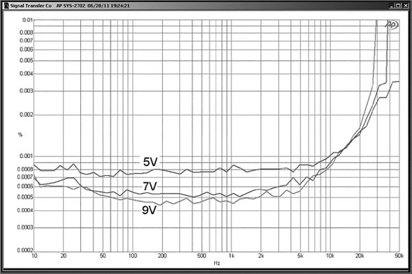
It is clear that the 5534A is not distortion free in this application. The LM4562 has superior linearity and load-driving capabilities in general, though we know that the noise performance with an MM cartridge will be inferior due to its higher current noise. The results for the LM4562 in Figure 9.15 are convincing.
The rise in distortion at LF has been completely eliminated, but disappointingly the HF distortion is barely improved at all. It is disconcerting that the opamp output is no more effective at driving the RIAA feedback network, given the excellent drive capabilities of the LM4562 into resistive loads. I suspect the reason is that the output stage uses VI limiting for overload protection, as opposed to the simple current-limiting used in the 5532, and this makes it more likely to come into action when driving a highly reactive load like an RIAA network, which above 1 kHz looks pretty much like a capacitance in series with a low-value resistor (R0) connected to ground. The use of a “helper” opamp to assist in driving the RIAA network would be likely to reduce the distortion; see Chapter 1. Figure 9.15 confirms that the LF distortion is wholly from the 5534 opamp and is nothing to do with capacitor distortion.
Conclusions
While MM RIAA cartridge noise is a complicated business, the clear result is that the 5534A is the cheapest and easiest way to get within 3 dB of the theoretical best noise performance. This is because it not only has low noise in general but also a favourable balance between its voltage noise and current noise for an MM source. It is a happy chance that it is inexpensive. To get within 2 dB of perfection, another 5532 can be added to implement load synthesis.
Money can be saved by using a 5532, but you are then 5 dB from theoretical best noise, and running two channels through the same package is very likely to compromise crosstalk.
For these reasons the 5534A is used in all the opamp designs in this book.
References
1. Lipshitz, S. P. “On RIAA Equalisation Networks” Journal of Audio Engineering Society, June 1979, p. 458, onwards.
2. Vogel, B. The Sound of Silence. 2nd edition. Springer, 2011, p. 523. ISBN 978-3-642-19773-d.
3. Langford-Smith, F. Radio Designer’s Handbook. 1953, Newnes reprint 1999, Chapter 17, p. 705. ISBN 0 7506 3635 1.
4. Vogel, B. Radio Designer’s Handbook. 1953, pp. 201–224.
5. Crossley, D. Personal Communication, Nov 2016.
6. Francis, E. H. “Moving Iron Pickups” Wireless World, Aug 1947, p. 285.
7. Vogel, B. “Adventure: Noise” (Calculating RIAA noise) Electronics World, May 2005, p. 28.
8. Al-Asadi et al. “A Simple Formula for Calculating the Frequency-Dependent Resistance of a Round Wire” Microwave and Optical Technology Letters, Volume 19, No. 2, Oct 5 1998, pp. 84–87.
9. Hallgren, B. “On the Noise Performance of a Magnetic Phonograph Pickup” Journal of Audio Engineering Society, Sept 1975, p. 546.
10. Elliot, Rod Elliott Sound Products: Sound.whsites.net/articles/cartridge-loading.html Accessed Nov 2016.
11. de Gevel van, M. “Noise and Moving-Magnet Cartridges” Electronics World, Oct 2003, p. 38.
12. Sherwin, J. “Noise Specs Confusing?” National Semiconductor Application Note AN-104” Linear Applications Handbook, 1991.
13. de Gevel van, M. Private Communication, Feb 1996.
14. Percival, W. S. “An Electrically ‘Cold’ Resistance” Wireless Engineering, Volume 16, May 1939, pp. 237–240.
15. Strutt, M. J. O., and Van der Ziel, A. “Suppression of Spontaneous Fluctuations in Amplifiers and Receiver for Electrical Communication and For Measuring Devices,” Physica, Volume 9, No. 6, June 1942, pp. 513–527.
16. Van der Ziel, A. Noise. New York: Prentice-Hall, 1954, pp. 262 et seq.
17. Holman, T. “New Factors in Phonograph Preamplifier Design” Journal of Audio Engineering Society, Volume 24, No. 4, May 1975, p. 263.
18. Hoeffelman, J. M., and Meys, Rene P. “Improvement of the Noise Characteristics of Amplifiers for Magnetic Transducers” Journal of Audio Engineering Society, Volume 26, No. 12, Dec 1978, p. 935.
19. Self, D. “Advanced Preamplifier Design” Wireless World, Nov 1976, pp. 41–46.