
Chapter 1
The Basics
Signals
An audio signal can be transmitted either as a voltage or a current. The construction of the universe is such that almost always the voltage mode is more convenient; consider for a moment an output driving more than one input. Connecting a series of high-impedance inputs to a low-impedance output is simply a matter of connecting them in parallel, and if the ratio of the output and input impedances is high there will be negligible variations in level. To drive multiple inputs with a current output it is necessary to have a series of floating current-sensor circuits that can be connected in series. This can be done,[1] as pretty much anything in electronics can be done, but it requires a lot of hardware and probably introduces performance compromises. The voltage-mode connection is just a matter of wiring.
Obviously, if there’s a current, there’s a voltage, and vice versa. You can’t have one without the other. The distinction is in the output impedance of the transmitting end (low for voltage mode, high for current mode) and in what the receiving end responds to. Typically, but not necessarily, a voltage input has a high impedance; if its input impedance was only 600 Ω, as used to be the case in very old audio distribution systems, it is still responding to voltage, with the current it draws doing so a side issue, so it is still a voltage amplifier. In the same way, a current input typically, but not necessarily, has a very low input impedance. Current outputs can also present problems when they are not connected to anything. With no terminating impedance, the voltage at the output will be very high, and probably clipping heavily; the distortion is likely to crosstalk into adjacent circuitry. An open-circuit voltage output has no analogous problem.
Current-mode connections are not common. One example is the Krell Current Audio Signal Transmission, (CAST) technology, which uses current-mode to interconnect units in the Krell product range. While it is not exactly audio, the 4–20 mA current loop format is widely used in instrumentation. The current-mode operation means that voltage drops over long cable runs are ignored, and the zero offset of the current (i.e. 4 mA = zero) makes cable failure easy to detect: if the current suddenly drops to zero, you have a broken cable.
The old DIN interconnection standard was a form of current-mode connection in that it had voltage output via a high output impedance, of 100 kΩ or more. The idea was presumably that you could scale the output to a convenient voltage by selecting a suitable input impedance. The drawback was that the high output impedance made the amount of power transferred very small, leading to a poor signal-to-noise ratio. The concept is now wholly obsolete.
Amplifiers
At the most basic level, there are four kinds of amplifier, because there are two kinds of signal (voltage and current) and two types of port (input and output). The handy word “port” glosses over whether the input or output is differential or single ended. Amplifiers with differential input are very common—such as all opamps and most power amps—but differential outputs are rare and normally confined to specialised telecoms chips.
Table 1.1 summarises the four kinds of amplifier:
| Amplifier type | Input | Output | Application |
|---|---|---|---|
Voltage amplifier |
Voltage |
Voltage |
General amplification |
Transconductance amplifier |
Voltage |
Current |
Voltage control of gain |
Current amplifier |
Current |
Current |
??? |
Transimpedance amplifier |
Current |
Voltage |
Summing amplifiers, DAC interfacing |
Voltage Amplifiers
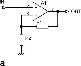
These are the vast majority of amplifiers. They take a voltage input at a high impedance and yield a voltage output at a low impedance. All conventional opamps are voltage amplifiers in themselves, but they can be made to perform as any of the four kinds of amplifier by suitable feedback connections. Figure 1.1a shows a high-gain voltage amplifier (e.g. opamp) with series voltage feedback. The closed-loop gain is (R1 + R2)/R2.
Transconductance Amplifiers
The name simply means that a voltage input (usually differential) is converted to a current output. It has a transfer ratio A = IOUT/VIN, which has dimensions of I/V or conductance, so it is referred to as a transconductance amplifier. It is possible to make a very simple, though not very linear, voltage-controlled amplifier with transconductance technology; differential-input operational transconductance amplifier (OTA) ICs have an extra pin that gives voltage control of the transconductance, which when used with no negative feedback gives gain control. Performance falls well short of that required for quality hi-fi or professional audio. Figure 1.1b shows an OTA used without feedback; note the current-source symbol at the output.
Current Amplifiers
These accept a current in and give a current out. Since, as we have already noted, current-mode operation is rare, there is not often a use for a true current amplifier in the audio business. They should not be confused with current-feedback amplifiers (CFAs) which have a voltage output, the “current” bit referring to the way the feedback is applied in current-mode.[2] The bipolar transistor is sometimes described as a current amplifier, but it is nothing of the kind. Current may flow in the base circuit, but this is just an unwanted side effect. It is the voltage on the base that actually controls the transistor. I have seen it stated that the Hall-effect multiplier is a current amplifier; this is wholly untrue, as the output is a voltage. A true current amplifier can be built by following a transimpedance amplifier with a transconductance amplifier, but this uses two separate stages, with a voltage as an intermediate quantity.

Transimpedance Amplifiers
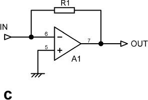
A transimpedance amplifier accepts a current in (usually single ended) and gives a voltage out. It is sometimes called an I-V converter. It has a transfer ratio A = VOUT/IIN, which has dimensions of V/I or resistance. That is why it is referred to as a transimpedance or transresistance amplifier. Transimpedance amplifiers are usually made by applying shunt voltage feedback to a high-gain voltage amplifier. The voltage amplifier stage (VAS) in most power amplifiers is a transimpedance amplifier. They are used for I-V conversion when interfacing to DACs with current outputs. Transimpedance amplifiers are sometimes incorrectly described as “current amplifiers”.
Figure 1.1c shows a high-gain voltage amplifier (e.g. opamp) transformed into a transimpedance amplifier by adding the shunt voltage feedback resistor R1. The transimpedance gain is simply the value of R1, though it is normally expressed in V/mA rather than ohms.
Negative Feedback
Negative feedback is one of the most useful and omnipresent concepts in electronics. It can be used to control gain, to reduce distortion, and improve frequency response, and to set input and output impedances, and one feedback connection can do all these things at the same time. Negative feedback comes in four basic modes, as in the four basic kinds of amplifier. It can be taken from the output in two different ways (voltage or current feedback) and applied to the amplifier input in two different ways (series or shunt). Hence there are four combinations.
However, unless you’re making something exotic like an audio constant-current source, the feedback is always taken as a voltage from the output, leaving us with just two feedback types, series and shunt, both of which are extensively used in audio. When series feedback is applied, as in Figure 1.1a, the following statements are true:
- Negative feedback reduces voltage gain.
- Negative feedback increases gain stability.
- Negative feedback increases bandwidth.
- Negative feedback increases amplifier input impedance.
- Negative feedback reduces amplifier output impedance.
- Negative feedback reduces distortion.
- Negative feedback does not directly alter the signal- to-noise ratio.
If shunt feedback is applied to a voltage amplifier to make a transimpedance amplifier, as in Figure 1.1c, all the above statements are still true, except since we have applied shunt rather than series negative feedback, the input impedance is reduced.
The basic feedback relationship is Equation 1.1 is dealt with at length in any number of textbooks, but it is of such fundamental importance that I feel obliged to include it here. The open-loop gain of the amplifier is A, and β is the feedback fraction, such that if in Figure 1.1a R1 is 2 kΩ and R2 is 1 kΩ, β is 1/3. If A is very high, you don’t even need to know it; The 1 on the bottom becomes negligible, and the A’s on top and bottom cancel out, leaving us with a gain of almost exactly three.
| 1.1 |
Negative feedback can however do much more than stabilising gain. Anything unwanted occurring in the amplifier, be it distortion or DC drift, or almost any of the other ills that electronics is heir to, is also reduced by the negative-feedback factor. (NFB factor for short) This is equal to:
| 1.2 |
What negative feedback cannot do is improve the noise performance. When we apply feedback the gain drops, and the noise drops by the same factor (or less), leaving the signal-to-noise ratio the same (or worse). Negative feedback and the way it reduces distortion is explained in much more detail in one of my other books.[3]
Nominal Signal Levels and Dynamic Range
The absolute level of noise in a circuit is not of great significance in itself—what counts is how much greater the signal is than the noise—in other words the signal to noise ratio. An important step in any design is the determination of the optimal signal level at each point in the circuit. Obviously a real signal, as opposed to a test sine wave, continuously varies in amplitude, and the signal level chosen is purely a nominal level. One must steer a course between two evils:
- If the signal level is too low, it will be contaminated unduly by noise.
- If the signal level is too high there is a risk it will clip and introduce severe distortion.
The wider the gap between them the greater the dynamic range. You will note that the first evil is a certainty, while the second is more of a statistical risk. The consequences of both must be considered when choosing a level. If the best possible signal-to-noise is required in a studio recording, then the internal level must be high, and if there is an unexpected overload you can always do another take. In live situations it will often be preferable use a lower nominal level and sacrifice some noise performance to give less risk of clipping.
If you seek to increase the dynamic range, you can either increase the maximum signal level or lower the noise floor. The maximum signal levels in opamp-based equipment are set by the voltage capabilities of the opamps used, and this usually means a maximum signal level of about 10 Vrms or +22 dBu. Discrete-transistor technology removes the absolute limit on supply voltage and allows the voltage swing to be at least doubled before the supply rail voltages get inconveniently high. For example, ±40V rails are quite practical for small-signal transistors and permit a theoretical voltage swing of 28 Vrms or +31 dBu. However, in view of the complications of designing your own discrete circuitry and the greater space and power it requires, those nine extra dB of headroom are dearly bought. You must also consider the maximum signal capabilities of stages downstream—they might get damaged.
The dynamic range of human hearing is normally taken as 100 dB, ranging from the threshold of hearing at 0 dB SPL to the usual “Jack hammer at 1 m” at +100 dB SPL; however, hearing damage is generally reckoned to begin with long exposures to levels above +80 dB SPL. There is, in a sense, a physical maximum to the loudest possible sound. Since sound is composed of cycles of compression and rarefaction, this limit is reached when the rarefaction creates a vacuum, because you can’t have a lower pressure than that. This corresponds to about +194 dB SPL. I thought this would probably be instantly fatal to a human being, but a little research showed that stun grenades generate +170 to +180 dB SPL, so maybe not. It is certainly possible to get asymmetrical pressure spikes higher than +194 dB SPL, but it is not clear that this can be defined as sound.
Compare this with the dynamic range of a simple piece of cable. Let’s say it has a resistance of 0.5 Ω; the Johnson noise from that will be −155 dBu. If we comply with the European Low Voltage Directive the maximum voltage will be 50 Vpeak = 35 Vrms = +33 dBu, so the dynamic range is 155 + 33 = 188 dB, which purely by numerical coincidence is close to the maximum sound level of 194 dB SPL.
Gain Structures
There are some very basic rules for putting together an effective gain structure in a piece of equipment. Like many rules, they are subject to modification or compromise when you get into a tight corner. Breaking them reduces the dynamic range of the circuitry, either by worsening the noise or restricting the headroom; whether this is significant depends on the overall structure of the system and what level of performance you are aiming at. Three simple rules are:
- 1) Don’t amplify then attenuate.
- 2) Don’t attenuate then amplify.
- 3) The signal should be raised to the nominal internal level as soon as possible to minimise contamination with circuit noise.
There are rare exceptions. For an example, see Chapter 11 on moving-coil disc inputs, where attenuation after amplification does not compromise headroom because of a more severe headroom limit downstream.
Amplification Then Attenuation
Put baldly it sounds too silly to contemplate, but it is easy to thoughtlessly add a bit of gain to make up for a loss somewhere else, and immediately a few dB of precious and irretrievable headroom are gone for good. This assumes that each stage has the same power rails and hence the same clipping point, which is usually the case in opamp circuitry.
Figure 1.2a shows a system with a gain control designed to keep 10 dB of gain in hand. In other words, the expectation is that the control will spend most of its working life set somewhere around its “0 dB” position, where it introduces 10 dB of attenuation, as is typically the case for a fader on a mixer. To maintain the nominal signal level at 0 dBu we need 10 dB of gain, and a +10 dB amplifier (Stage 2) has been inserted just before the gain control. This is not a good decision. This amplifier will clip 10 dB before any other stage in the system and introduces what one might call a headroom bottleneck.
There are exceptions. The moving-coil phono head amp described in Chapter 11 appears to flagrantly break this rule, as it always works at maximum gain even when this is not required. But when considered in conjunction with the following RIAA stage, which also has considerable gain, it makes perfect sense, for the stage gains are configured so that the second stage always clips first, and there is actually no loss of headroom.
Attenuation Then Amplification
In Figure 1.2b the amplifier is now after the gain control, and noise performance rather than headroom suffers. If the signal is attenuated, any active device will inescapably add noise in restoring the level. Every conventional gain-control block has to address this issue. If we once more require a gain variable from +10 dB to off, i.e. minus infinity dB, as would be typical for a fader or volume control, then usually the potentiometer is placed before the gain stage, as in Figure 1.2b, because as a rule some loss in noise performance is more acceptable than a permanent 10 dB reduction in system headroom. If there are options for the amplifier stages in terms of a noise/cost trade-off (such as using the 5532 versus a TL072) and you can only afford one low-noise stage, then it should be Stage 2.


If all stages have the same noise performance this configuration is 10 dB noisier than the previous version when gain is set to 0 dB.
Raising the Input Signal to the Nominal Level
Getting the incoming signal up to the nominal internal level right away in one jump is almost always preferable as it gives the best noise performance. Sometimes when large amounts of gain are required it is better done in two amplifier stages; typical examples are microphone preamps with wide gain ranges and phono preamps that insist on performing the RIAA equalisation in several goes. (The latter are explored in Chapter 5.) In these cases the noise contribution of the second stage may be significant.
Consider a signal path which has, say, an input of −10 dBu and a nominal internal level of 0 dBu, and so needs an overall gain of +10 dB:
- 1) The first version in Figure 1.3a has an input amplifier, Amp 1, with +10 dB of gain followed by two unity-gain circuit blocks, A and B. These might for example be lowpass and highpass Sallen and Key filters for bandwidth definition; see Chapter 13. All circuit blocks are assumed to have equivalent input noise at −100 dBu, so the first stage in Figure 1.3a has a noise output of −100 + 10 = −90 dBu. At the output of A the noise is the rms-sum of the −90 dBu input and the −100 dBu from A, giving −89.6 dBu. At the output of B another −100 dBu has been rms-added, so the final noise output is −89.2 dBu. It is clear that A and B have contributed little to the final noise, due to the raised level of the signal when it passes through them.
- 2) Now take a second version of the signal path that has an input amplifier Amp 1 with +5 dB of gain, followed by block A, another amplifier with 5 dB of gain, then block B. See Figure 1.3b. The noise output is now −87.6 dB, 1.6 dB worse, because the noise from A has now been amplified by +5 dB in Amp 2. There are also more parts, and the second version appears to be clearly an inferior design. Usually it would be, but there can be good reasons for splitting up gain into two stages; if the distortion performance is critical, then using two stages with +5 dB of closed-loop gain rather than +10 dB means that each stage has 5 dB more negative feedback and lower distortion. This approach can be refined by not splitting the gain in half but putting more in the first stages where the signal levels and hence the distortion will be lower. This technique was used very successfully in my multitude-of-opamps power amplifier, published in Elektor;[4] the first stage had a gain of +11 dB and the second +6 dB. If amplification is done in two stages, then for the lowest noise they should come first in the signal path and not have block A put between them.
- 3) Third version in Figure 1.3c puts both A and B unity- gain stages between Amp 1 and Amp 2. The noise from both A and B is now amplified by +5 dB by Amp 2, and so the noise output is increased to −87.1 dBu. This is only 0.5 dB worse than Case 2, as a consequence of how rms-addition works; putting A before Amp 2 has already done most of the damage.
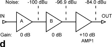
- 4) It is now fairly clear that putting A and B first, and then following them with a single +10 dB amplifier stage, as in Figure 1.3d, will give the highest output noise yet, and so it does, as the noise from both A and B is amplified by +10 dB. The noise out is now −84.0 dBu, 5.2 dB worse than Case 1. And all we have done is alter the order of the stages.
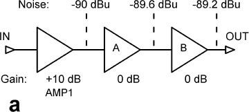


I think this demonstrates effectively that signals should always be amplified to their nominal internal level as soon as possible.
Active Gain Controls
The previous section should not be taken to imply that noise/headroom performance must always be sacrificed when a gain control is included in the signal path. This is not so. If we move beyond the idea of a fixed-gain block and recognise that the amount of gain present can be varied, then less gain when the maximum is not required will reduce the noise generated. For volume-control purposes it is essential that the gain can be reduced to near zero, though it is not necessary for it to be as firmly “off ” as the faders or sends of a mixer.
An active volume-control stage gives lower noise at lower volume settings because there is less gain. The Baxandall active configuration also gives excellent channel balance because it depends solely on the mechanical alignment of a dual linear pot—all mismatches of its electrical characteristics are cancelled out, and there are no quasi-log dual slopes to induce anxiety.
Active gain controls are looked at in depth in Chapter 4.
Noise and Its Colours
Noise here refers only to the random noise generated by resistances and active devices. The term is sometimes used to include mains hum, spurious signals from demodulated RF, and other nonrandom sources, but this threatens confusion, and I prefer to call the other unwanted signals “interference”. In one case we strive to minimise the random variations arising in the circuit itself, in the other we are trying to keep extraneous signals out, and the techniques are wholly different.
When noise is referred to in electronics it means white noise unless it is specifically labelled as something else, because that is the form of noise that most electronic processes generate. There are two elemental noise mechanisms which make themselves felt in all circuits and active devices. These are Johnson noise and Shot noise, which are both forms of white noise. Both have Gaussian probability density functions. These two basic mechanisms generate the noise in both BJTs and FETs, though in rather different ways.
There are other forms of noise that originate from less fundamental mechanisms such as device processing imperfections, which do not have a white spectrum; examples are 1/f (flicker) noise and popcorn noise. These noise mechanisms are described later in this chapter.
Nonwhite noise is given a colour which corresponds to the visible spectrum; thus red noise has a larger low-frequency content than white noise, while pink is midway between the two.
White noise has equal power in equal absolute bandwidth, i.e. with the bandwidth measured in Hz. Thus there is the same power between 100 and 200 Hz as there is between 1100 and 1200 Hz. It is the type produced by most electronic noise mechanisms.[5]
Pink noise has equal power in equal ratios of bandwidth, so there is the same power between 100 and 200 Hz as there is between 200 and 400 Hz. The energy per Hz falls at 3 dB per octave as frequency increases; i.e. the power density is proportional to 1/f. Pink noise is widely used for acoustic applications like room equalisation and loudspeaker measurement as it gives a flat response when viewed on a third-octave or other constant-percentage-bandwidth spectrum analyser.[6]
Red noise has energy per Hz falling at 6 dB per octave rather than 3, the power density proportional to 1/f2. It is important in the study of stochastic processes and climate models, but has little application in audio. The only place you are likely to encounter it is in the oscillator section of analogue synthesisers. It is sometimes called Brownian noise as it can be produced by Brownian motion, hence its alternative name of random-walk noise. Brown here is a person and not a colour.[7]
Blue noise has energy per Hz rising at 3 dB per octave. The power density is proportional to f. Blue noise is used for dithering in image anti-aliasing, but has, as far as I am aware, no application to audio. The spectral density of blue noise is proportional to the frequency. It appears that the light-sensitive cells in the retina of the mammalian eye are arranged in a pattern that resembles blue noise.[8] Great stuff, this evolution.
Violet noise has energy per Hz rising at 6 dB per octave. (I imagine you saw that one coming.) The power density is proportional to f 2. It is also known as “differentiated white noise” as a differentiator circuit has a frequency response rising at 6 dB per octave. Sometimes called purple noise. A real-life source of violet noise is the acoustic thermal noise of water; at high frequencies it dominates hydrophone reception.
Grey noise is pink noise modified by a psychoacoustic equal loudness curve, such as the inverse of the A-weighting curve, to give the perception of equal loudness at all frequencies.
Green noise really does exist, though not in the audio domain. It is used for stochastic half-toning of images and consists of binary dither patterns composed of homogeneously distributed minority pixel clusters. Another definition is pink noise with increased levels around 500 Hz; for background noise generators and the like, this is supposed to more closely resemble the noise of the natural environment (i.e. without man-made noise like road traffic, aeroplanes, etc.).
Black noise also has some kind of existence. One definition of black noise is the absence of noise, i.e. silence; I do not think this is very useful. Another definition is noise with the spectrum of black-body radiation; it has nothing to do with audio.
Johnson Noise
Johnson noise is produced by all resistances, including those real resistances hiding inside transistors (such as rbb, the base spreading resistance). It is not generated by the so-called intrinsic resistances, such as re, which are an expression of the Vbe/Ic slope and not a physical resistance at all. Given that Johnson noise is present in every circuit and often puts a limit on noise performance, it is perhaps a bit surprising that it was not discovered until 1928 by John B. Johnson at Bell Labs.[9] The likely reason is that the valves of the day were very much noisier than the resistors.
The rms amplitude of Johnson noise is easily calculated with the classic formula:
| 1.3 |
Where:
vn is the rms noise voltage
T is absolute temperature in °K
B is the bandwidth in Hz
k is Boltzmann’s constant
R is the resistance in Ohms
The only thing to be careful with here (apart from the usual problem of keeping the powers of ten straight) is to make sure you use Boltzmann’s constant (1.380662 × 10⁻²³), and NOT the Stefan-Boltzmann constant (5.67 10−08), which relates to black-body radiation and will give some spectacularly wrong answers. Often the voltage noise is left in its squared form for ease of summing with other noise sources. Table 1.2 gives a feel for how resistance affects the magnitude of Johnson noise. The temperature is 25 °C and the bandwidth is 22 kHz.
Johnson noise theoretically goes all the way to daylight, and presumably even further up to gamma-ray frequencies, but in the real world is ultimately band-limited by the shunt capacitance of the resistor. Johnson noise is not produced by circuit reactances—i.e. pure capacitance and inductance. In the real world, however, reactive components are not pure, and the winding resistances of transformers can produce significant Johnson noise; this is an important factor in the design of moving-coil cartridge step-up transformers. Capacitors with their very high leakage resistances approach perfection much more closely, and the capacitance has a filtering effect. They usually have no detectable effect on noise performance, and in some circuitry it is possible to reduce noise by using a capacitive potential divider instead of a resistive one.[10]
The noise voltage is of course inseparable from the resistance, so the equivalent circuit is of a voltage source in series with the resistance present. While Johnson noise is usually represented as a voltage, it can also be treated as a Johnson noise current, by means of the Thevenin-Norton transformation, which gives the alternative equivalent circuit of a current source in shunt with the resistance. The equation for the noise current is simply the Johnson voltage divided by the value of the resistor it comes from in = vn/R.
| Resistance Ohms Ω | Noise voltage uV | Noise voltage dBu | Application |
|---|---|---|---|
1 |
0.018 |
−152.2 dBu |
Movinoil cartridge impedance (low output) |
3.3 |
0.035 |
−147.0 dBu |
Movinoil cartridge impedance (medium output) |
10 |
0.060 |
−142.2 dBu |
Movinoil cartridge impedance (high output) |
47 |
0.13 |
−135.5 dBu |
Line output isolation resistor |
68 |
0.16 |
−133.9 dBu |
Line output isolation resistor |
100 |
0.19 |
−132.2 dBu |
Output isolation or feedback network |
150 |
0.23 |
−130.4 dBu |
Dynamic microphone source impedance |
200 |
0.27 |
−129.2 dBu |
Dynamic microphone source impedance (older) |
250 |
0.30 |
−128.2 dBu |
Worsase output impedance of 1 kΩ pot |
300 |
0.33 |
−127.4 dBu |
Typical value in lompedance design |
400 |
0.38 |
−126.2 dBu |
Typical value in lompedance design |
500 |
0.43 |
−125.2 dBu |
Worsase output impedance of 2 kΩ pot |
600 |
0.47 |
−124.4 dBu |
The ancient matcheine impedance |
700 |
0.50 |
−123.7 dBu |
Typical MM cartridge resistance |
800 |
0.54 |
−123.2 dBu |
Typical value in lompedance design |
1000 |
0.60 |
−122.2 dBu |
A nice round number |
1200 |
0.66 |
−121.4 dBu |
Typical value in lompedance design |
1250 |
0.67 |
−121.2 dBu |
Worsase output impedance of 5 kΩ pot |
1500 |
0.74 |
−120.4 dBu |
Typical value in lompedance design. E12 |
2000 |
0.85 |
−119.2 dBu |
Typical value in lompedance design. E24 |
2500 |
0.95 |
−118.2 dBu |
Worsase output impedance of 10 kΩ pot |
5000 |
1.35 |
−115.2 dBu |
Worsase output impedance of 20 kΩ pot |
12500 |
2.13 |
−111.2 dBu |
Worsase output impedance of 50 kΩ pot |
25000 |
3.01 |
−108.2 dBu |
Worsase output impedance of 100 kΩ pot |
1 mega (106) |
19.0 |
−92.2 dBu |
Another nice round number |
1 giga (109) |
601 |
−62.2 dBu |
As used in capacitor microphone amplifiers |
1 tera (1012) |
1900 |
−32.2 dBu |
Insulation testers read in terhms |
1 peta (1015) |
601,281 |
−2.2 dBu |
OK, it’s getting silly now |
When it is first encountered, this ability of resistors to generate electricity from out of nowhere seems deeply mysterious. You wouldn’t be the first person to think of connecting a small electric motor across the resistance and getting some useful work out—and you wouldn’t be the first person to discover it doesn’t work. If it did, then by the First Law of Thermodynamics (the law of conservation of energy) the resistor would have to get colder, and such a process is flatly forbidden by … the Second Law of Thermodynamics. The Second Law is no more negotiable than the First Law, and it says that energy cannot be extracted by simply cooling down one body. If you could, it would be what thermodynamicists call a Perpetual Motion Machine of the Second Kind, and they are no more buildable than the more familiar Perpetual Motion Machine of the First Kind, which if it existed would make energy out of nowhere.
It is interesting to speculate what happens as the resistor is made larger. Does the Johnson voltage keep increasing, until there is a hazardous voltage across the resistor terminals? Obviously not, or picking up any piece of plastic would be a lethal experience. Johnson noise comes from a source impedance equal to the resistor generating it, and this alone would prevent any problems. Table 1.2 ends with a couple of silly values to see just how this works; the square root in the equation means that you need a petaohm resistor (1 × 10¹⁵ Ω) to reach even 600 mV rms of Johnson noise. Resistors are made up to at least 100 GΩ, but petaohm resistors (PΩ?) would really be a minority interest.
Shot Noise
It is easy to forget that an electric current is not some sort of magic fluid but is actually composed of a finite though usually very large number of electrons, so current is in effect quantised. Shot noise is so called because it allegedly sounds like a shower of lead shot being poured onto a drum, and the name emphasises the discrete nature of the charge carriers. Despite the picturesque description the spectrum is still that of white noise, and the noise current amplitude for a given steady current is described by a surprisingly simple equation (as Einstein said, the most incomprehensible thing about the universe is that it is comprehensible) that runs thus:
| 1.4 |
Where:
q is the charge on an electron (1.602 × 10⁻¹⁹ coulomb)
Idc is the mean value of the current
B is the bandwidth examined
As with Johnson noise, often the shot noise is left in its squared form for ease of summing with other noise sources. Table 1.3 helps to give a feel for the reality of shot noise. As the current increases, the shot noise increases too, but more slowly as it depends on the square root of the DC current; therefore the percentage fluctuation in the current becomes less. It is the small currents which are the noisiest.
The actual level of shot noise voltage generated if the current noise is assumed to flow through a 100 ohm resistor is rather low, as the last column shows. Certainly there are many systems which will be embarrassed by an extra noise source of −99 dBu, but to generate this level of shot noise requires 1 amp to flow through 100 ohms, which naturally means a voltage drop of 100 V and 100 watts of power dissipated. These are not often the sort of circuit conditions that exist in preamplifier circuitry. This does not mean that shot noise can be ignored completely, but it can usually be ignored unless it is happening in an active device where the shot noise is amplified.
1/f Noise (Flicker Noise)
This is so called because it rises in amplitude proportionally as the frequency examined falls. Unlike Johnson noise and shot noise, it is not a fundamental consequence of the way the universe is put together, but the result of imperfections in device construction. Flicker noise appears in all kinds of active semiconductors, and also in some types of resistor. When 1/f noise exists, as frequency falls the total noise density stays level down to the 1/f corner frequency, after which it rises at 6 dB/octave. This can frequently be seen in opamp spec-sheets. For a discussion of flicker noise in resistors see Chapter 2.
Popcorn Noise
This form of noise is named after the sound of popcorn being cooked, not eaten. It is also called burst noise or bistable noise and is a type of low-frequency noise that is found primarily in integrated circuits, appearing as low-level step changes in the output voltage, occurring at random intervals. Viewed on an oscilloscope this type of noise shows bursts of changes between two or more discrete levels. The amplitude stays level up to a corner frequency, at which point it falls at a rate of 1/f2. Different burst-noise mechanisms within the same device can exhibit different corner frequencies. The exact mechanism is poorly understood, but is known to be related to the presence of heavy-metal ion contamination, such as gold. As for 1/f noise, the only measure that can be taken against it is to choose an appropriate device. Like 1/f noise, popcorn noise does not have a Gaussian amplitude distribution.

Summing Noise Sources
When random noise from different sources is summed, the components do not add in a 2 + 2 = 4 manner. Since the noise components come from different sources, with different versions of the same physical processes going on, they are uncorrelated and will partially reinforce and partially cancel, so root-mean-square (rms) addition holds, as shown in Equation 1.5. If there are two noise sources with the same level, the increase is 3 dB rather than 6 dB. When we are dealing with two sources in one device, such as a bipolar transistor, the assumption of no correlation is slightly dubious, because some correlation is known to exist, but it does not seem to be enough to cause significant calculation errors.
| 1.5 |
Any number of noise sources may be summed in the same way by simply adding more squared terms inside the square root, as shown by the dotted lines. When dealing with noise in the design process, it is important to keep in mind the way that noise sources add together when they are not of equal amplitude. Table 1.4 shows how this works in decibels. Two equal voltage noise sources give a sum of +3 dB, as expected. What is notable is that when the two sources are of rather unequal amplitude, the smaller one makes very little contribution to the result.
| Source 1 dB | Source 2 dB | dB sum |
|---|---|---|
0 |
0 |
+3.01 |
0 |
−1 |
+2.54 |
0 |
−2 |
+2.12 |
0 |
−3 |
+1.76 |
0 |
−4 |
+1.46 |
0 |
−5 |
+1.19 |
0 |
−6 |
+0.97 |
0 |
−10 |
+0.41 |
0 |
−15 |
+0.14 |
0 |
−20 |
+0.04 |
If we have a circuit in which one noise source is twice the rms amplitude of the other, (a 6 dB difference) then the quieter source only increases the rms-sum by 0.97 dB, a change barely detectable on critical listening. If one source is 10 dB below the other, the increase is only 0.4 dB, which in most cases could be ignored. At 20 dB down, the increase is lost in measurement error. This mathematical property of uncorrelated noise sources is exceedingly convenient, because it means that in practical calculations we can neglect all except the most important noise sources with minimal error. Since all semiconductors have some variability in their noise performance, it is rarely worthwhile to make the calculations to great accuracy.
Noise in Amplifiers
There are basic principles of noise design that apply to all amplifiers, be they discrete or integrated, single ended or differential. Practical circuits, even those consisting of an opamp and two resistors, have multiple sources of noise. Typically one source of noise will dominate, but this cannot be taken for granted and it is essential to evaluate all the sources and the ways that they add together if a noise calculation is going to be reliable. Here I add the complications one stage at a time.
Figure 1.4 shows that most useful of circuit elements, the perfect noiseless amplifier (these seem to be unaccountably hard to find in catalogues). It is assumed to have a definite gain A, without bothering about whether it is achieved by feedback or not, and an infinite input impedance. To emulate a real amplifier noise sources are concentrated at the input, combined into one voltage noise source and one current noise source. These can represent any number of actual noise sources inside the real amplifier. Figure 1.4 shows two ways of drawing the same situation.
It does not matter on which side of the voltage source the current source is placed; the “perfect” amplifier has an infinite input impedance, and the voltage source a zero impedance, so either way all of the current noise flows through whatever is attached to the input.
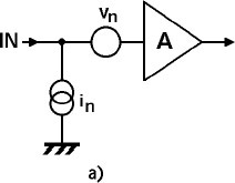
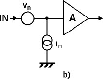
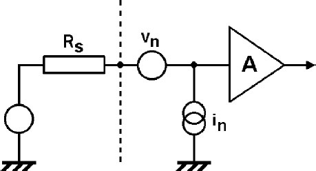
Figure 1.5 shows the first step to a realistic situation, with a signal source now connected to the amplifier input. The signal source is modelled as a perfect zero-impedance voltage source, with added series resistance Rs. Many signal sources are modelled accurately enough for noise calculations in this way. Examples are low-impedance dynamic microphones, moving-coil phono cartridges, and most electronic outputs. In others cases, such as moving-magnet phono cartridges and capacitor microphone capsules, there is a big reactive component which has a major effect on the noise behaviour and cannot be ignored or treated as a resistor. The magnitude of the reactances tends to vary from one make to another, but fortunately the variations are not usually large enough for the circuit approach for optimal noise to vary greatly. It is pretty clear that a capacitor microphone will have a very high source impedance at audio frequencies and will need a special high-impedance preamplifier to avoid low-frequency roll-off. It is perhaps less obvious that the series inductance of a moving-magnet phono cartridge becomes the dominating factor at the higher end of the audio band, and designing for the lowest noise with the 600 Ω or so series resistance alone will give far from optimal results. This is dealt with in Chapter 11.
There are two sources of voltage noise in the circuit of Figure 1.5.
- 1) The amplifier voltage noise source vn at the input.
- 2) The Johnson noise from the source resistance Rs.
These two voltage sources are in series and sum by rms-addition because they are uncorrelated.
There is only one current noise component; the amplifier noise current source in across the input. This generates a noise voltage when its noise current flows through Rs. (It cannot flow into the amplifier input because we are assuming an infinite input impedance.) This third source of voltage noise is also added in by rms-addition, and the total is amplified by the voltage gain A and appears at the output. The noise voltage at the input is the equivalent input noise (EIN). This is impossible to measure, so the noise at the amplifier output is divided by A to get the EIN. Having got this, we can compare it with the Johnson noise from the source resistance Rs; with a noiseless amplifier there would be no difference, but in real life the EIN will be higher by a number of dB, which is called the noise figure (NF). This gives a concise way of assessing how noisy our amplifier is and if it is worth trying to improve it. Noise figures very rarely appear in hi-fi literature, probably because most of them wouldn’t look very good; some would look the utter rubbish that they are. For the fearless application of noise figures to phono cartridge amplifiers see Chapters 9 and 11.
Noise in Phono Amplifiers
There are two basic noise situations in phono circuitry. A moving-magnet (MM) cartridge has high inductance, and as a result at HF much of the noise is generated by input device current noise and Johnson noise from the 47 kΩ loading resistor Rin rather than the resistance of the cartridge. The frequency-dependent impedance of the inductance makes things complicated. A reasonable rule is to design for minimum noise using the cartridge impedance at 3852 Hz, which will give near-optimal RIAA-equalised noise.[11] At this frequency a typical MM cartridge will have an impedance of around 10 kΩ. Chapter 9 gives much more detail on MM phono amplifier noise.
In contrast, moving-coil (MC) cartridges generally act as low-value resistances with minimal series inductance, and so the design approach for low noise is quite different. Voltage noise is all-important, and the effect of current noise and Johnson noise from any loading resistor is usually negligible. Chapter 11 gives much more detail on MC phono amplifier noise.
All the other parts of a phono amplifier system, such as flat amplification or subsonic filtering, usually operate under favourable impedance conditions comparable with MC inputs.
Noise in Bipolar Transistors
An analysis of the noise behaviour of discrete bipolar transistors can be found in many textbooks, so this is something of a quick summary of the vital points. Two important transistor parameters for understanding noise are rbb, the base spreading resistance, and re, the intrinsic emitter resistance. The first, rbb, is a real physical resistance—what is called an extrinsic resistance. The second parameter, re, is an expression of the Vbe/Ic slope and not a physical resistance at all, so it is called an intrinsic resistance.
Noise in bipolar transistors, as in amplifiers in general, is best dealt with by assuming a noiseless transistor with a theoretical noise voltage source in series with the base and a theoretical noise current source connected from base to emitter. These sources are usually described simply as the “voltage noise” and the “current noise” of the transistor.
Bipolar Transistor Voltage Noise
The voltage noise vn is made up of two components:
- The Johnson noise generated in the base spreading resistance rbb.
- The collector current (Ic) shot noise creating a noise voltage across re, the intrinsic emitter resistance.
These two components can be calculated from the equations given earlier and rms-summed thus:
| 1.6 |
Where:
k is Boltzmann’s constant (1.380662 × 10⁻²³)
q is the charge on an electron (1.602 × 10⁻¹⁹ coulomb)
T is absolute temperature in °K
Ic is the collector current
rbb is the base resistance in ohms
The first part of this equation is the usual expression for Johnson noise and is fixed for a given transistor type by the physical value of rbb, so the lower this is the better. The only way you can reduce this is by changing to another transistor type with a lower rbb or using paralleled transistors. The absolute temperature is a factor; running your transistor at 25 °C rather than 125 °C reduces the Johnson noise from rbb by 1.2 dB. Input devices usually run cool, but this may not be the case with moving-coil preamplifiers, where a large Ic is required, so it is not impossible that adding a heatsink would give a measurable improvement in noise.
The second (shot noise) part of the equation decreases as collector current Ic increases; this is because as Ic increases, re decreases proportionally, following re = 25/Ic where Ic is in mA. The shot noise however is only increasing as the square root of Ic, and the overall result is that the total vn falls—though relatively slowly—as collector current increases, approaching asymptotically the level of noise set by first part of the equation. There is an extra voltage noise source resulting from flicker noise produced by the base current flowing through rbb; this is only significant at high collector currents and low frequencies due to its 1/f nature and is not usually included in design calculations unless low-frequency quietness is a special requirement.
Bipolar Transistor Current Noise
The current noise, in, is mainly produced by the shot noise of the steady current Ib flowing through the transistor base. This means it increases as the square root of Ib increases. Naturally Ib increases with Ic. Current noise is given by
| 1.7 |
Where:
q is the charge on an electron
Ib is the base current
So, for a fixed collector current, you get less current noise with high-beta transistors because there is less base current.
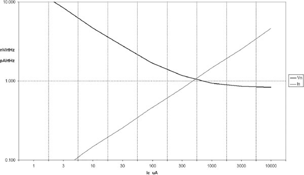
The existence of current noise as well as voltage noise means it is not possible to minimise transistor noise just by increasing the collector current to the maximum value the device can take. Increasing Ic reduces voltage noise, but it increases current noise, as in Figure 1.6. There is an optimum collector current for each value of source resistance, where the contributions are equal. Because both voltage and current noise are proportional to the square root of Ic, they change slowly as it alters, and the combined noise curve is rather flat at the bottom. There is no need to control collector current with great accuracy to obtain optimum noise performance.
I must emphasise that this is a simplified noise model. In practice both voltage and current noise densities vary with frequency. I have also ignored 1/f noise. However, it gives the essential insight into what is happening and leads to the right design decisions, so we will put our heads down and press on.
A quick example shows how this works. In a voltage amplifier we want the source impedances seen by the input transistors to be as low as possible, to minimise Johnson noise from them and to minimise the effects of input device current noise flowing through them. In a typical bit of circuitry using low-impedance design it may be 100 Ω. How do we minimise the noise from a single transistor faced with a 100 Ω source resistance?
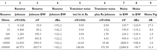
We assume the temperature is 25 °C, the bandwidth is 22 kHz, the rbb of our transistor is 40 Ω and its hfe (beta) is a healthy 150. Set Ic to 1 mA, which is plausible for an amplifier input stage, step the source resistance from 1 to 100,000 Ω in decades, and we get Table 1.5.
Column 1 shows the source resistance, and Column 2 the Johnson noise density it generates by itself. Factor in the bandwidth, and you get Columns 3 and 4, which show the voltage in nV and dBu respectively.
Column 5 is the noise density from the transistor, the rms-sum of the voltage noise and the voltage generated by the current noise flowing in the source resistance. Column 6 gives total noise density when we sum the source resistance noise density with the transistor noise density. Factor in the bandwidth again, and the resultant noise voltage is given in Columns 7 and 8. The final column (9) gives the noise figure (NF), which is the amount by which the combination of transistor and source resistance is noisier than the source resistance alone. In other words, it tells how close we have got to perfection, which would be a noise figure of 0 dB. The results for the 100 Ω source show that the transistor noise is less than the source resistance Johnson noise; there is little scope for improving things by changing transistor type or operating conditions.
The results for the other source resistances are worth looking at. The lowest source resistance considered is 1 Ω, representing a low-output MC cartridge. This gives the lowest noise output, (−134.9 dBu) as you would expect, but the NF is very poor at 17.3 dB, because the rbb at 40 Ω is generating a lot more noise than the 1 Ω source. This gives you some idea why it is hard to design quiet moving-coil head amplifiers. The best noise figure and the closest approach to theoretical perfection is with a 1000 Ω source, attained with a greater noise output than 100 Ω; it is essential to remember that the lowest NF does not mean the lowest noise output. As source resistance increases further, NF worsens again; a transistor with Ic = 1 mA has relatively high current noise and performs poorly with high source resistances.
Since Ic is about the only thing we have any control over here, let’s try altering it. If we increase Ic to 3 mA we find that for a 100 Ω source resistance, our amplifier is only a marginal 0.2 dB quieter. See Table 1.6, which skips the intermediate calculations and just gives the output noise and NF.
At 3 mA the noise with a 1 Ω source is 0.7 dB better, due to slightly lower voltage noise, but with 100 kΩ noise is higher by no less than 9.8 dB as the current noise is much increased.
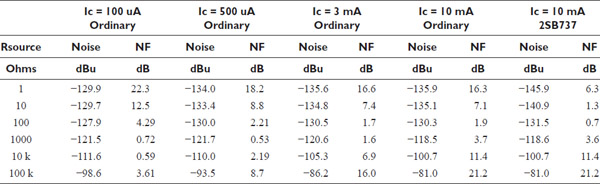
If we increase Ic to 10 mA, this makes the 100 Ω noise worse again, and we have lost that slender 0.2 dB improvement.
At 1 Ω the noise is 0.3 dB better, which is not exactly a breakthrough, and for the higher source resistances things worse again, the 100 kΩ noise increasing by another 5.2 dB. It therefore appears that a collector current of 3 mA is actually pretty much optimal for noise with our 100 Ω source resistance.
If we now pluck out our “ordinary” transistor and replace it with a specialised low-rbb part like the much-lamented 2SB737, with its a superbly low rbb of 2 Ω, the noise output at 1 Ω plummets by 10 dB, showing just how important low rbb is for moving-coil head amplifiers. The improvement for the 100 Ω source resistance is much less at 1.0 dB.
If we go back to the ordinary transistor and reduce Ic to 100 uA, we get the last two columns in Table 1.6. Compared with Ic = 3 mA, noise with the 1 Ω source worsens by 5.7 dB, and with the 100Ω source by 2.6 dB, but with the 100 kΩ source there is a hefty 12.4 dB improvement, due to reduced current noise. Quiet BJT inputs for high source impedances can be made by using low collector currents, but JFETs usually give better noise performance under these conditions.
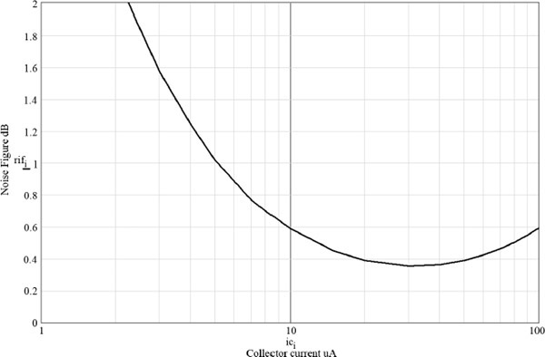
Finally we will look at a source impedance of around 10 kΩ, which is a reasonable design target for noise optimisation with most MM cartridges. Our ordinary transistor with Ic = 3 mA (Note no RIAA equalisation is being applied to any of these calculations—see Chapter 9 for that) gives −105.3 dBu, with an NF of 6.9 dB; not quiet. Reducing Ic to 500 uA drops the NF to a more respectable 2.2 dB, and reducing it drastically to 100uA drops it again to 0.6 dB. Obviously you have to have some collector current, but it looks as though reducing it even further might be rewarding. Figure 1.7 shows how the calculated noise figure for 10 kΩ source resistance reaches a shallow minimum just below 0.4 dB around collector currents of 20–50 uA. It is clear that MM cartridges running into BJT input devices require low collector currents.
The transistor will probably be the major source of noise in the circuit, but other sources may need to be considered. The transistor may have a collector resistor of high value, to optimise the stage gain, and this naturally introduces its own Johnson noise. Most discrete- transistor amplifiers have multiple stages, to get enough open-loop gain for linearisation by negative feedback, and an important consideration in discrete noise design is that the gain of the first stage should be high enough to make the noise contribution of the second stage negligible. This can complicate matters considerably. Precisely the same situation prevails in an opamp, but here someone else has done the worrying about second- stage noise for you, and the noise is specified for the complete part.
Noise in JFETs
JFETs operate completely differently from bipolar transistors, and noise arises in different ways. The voltage noise in JFETs arises from the Johnson noise produced by the channel resistance, the effective value of which is the inverse of the transconductance (gm) of the JFET at the operating point we are looking at. An approximate but widely accepted equation for this noise is :
| 1.8 |
Where:
k is Boltzmann’s constant (1.380662 × 10⁻²³)
T is absolute temperature in °K
FET transconductance goes up proportionally to the square root of drain current Id. When the transconductance is inserted into Equation 1.8, it is again square-rooted, so the voltage noise is proportional to the fourth root of drain current and varies with it very slowly. There is thus little point in using high drain currents.
The only current noise source in a JFET is the shot noise associated with the gate leakage current. Because the leakage current is normally extremely low, the current noise is very low, which is why JFETs give a good noise performance with high source resistances. However, don’t let the JFET get hot, because gate leakage doubles with each 10 °C rise in temperature; this is why JFETs can actually show increased noise if the drain current is increased to the point where they heat up.
The gm of JFETs is rather variable, but at Id = 1 mA ranges over about 0.5 to 3 mA/V (or mMho) so the voltage noise density varies from 4.7 to 1.9 nV/rtHz. Comparing this with Column 5 in Table 1.5, we can see that the BJTs are much quieter except at high source impedances, where their current noise makes them noisier than JFETs.
However, if you are prepared to use multiple devices, the lowest possible noise may be given by JFETs, because the voltage noise falls faster than the effect of the current noise rises when more devices are added. A low-noise laboratory amplifier design by Samuel Groner achieves a spectacularly low-noise density of 0.39 nV/rtHz by using eight paralleled JFETs.[12]
Noise in Opamps
The noise behaviour of an opamp is very similar to that of a single input amplifier, the difference being that there are now two inputs to consider and usually more associated resistors.
An opamp is driven by the voltage difference between its two inputs, and so the voltage noise can be treated as one voltage vnconnected between them. See Figure 1.8, which shows a differential amplifier.
Opamp current noise is represented by two separate current generators, in+ and in−, one in parallel with each input. These are assumed to be equal in amplitude and not correlated with each other. It is also assumed that the voltage and current noise sources are likewise uncorrelated, so that rms-addition of their noise components is valid. In reality things are not quite so simple and there is some correlation, and the noise produced can be slightly higher than calculated. In practice the difference is small compared with natural variations in noise performance.
Calculating the noise is somewhat more complex than for the simple amplifier of Figure 1.4. You must:
- 1) Calculate the voltage noise from the voltage noise density.
- 2) Calculate the two extra noise voltages resulting from the noise currents flowing through their associated components.
- 3) Calculate the Johnson noise produced by each resistor.
- 4) Allow for the noise gain of the circuit when assessing how much each noise source contributes to the output.
- 5) Add the lot together by rms-addition.
There is no space to go through a complete calculation, but here is a quick example:
Suppose you have an inverting amplifier like that in Figure 1.11a. This is simpler because the noninverting input is grounded, so the effect of in+ disappears, as it has no resistance to flow through and cannot give rise to a noise voltage. This shunt-feedback stage has a “noise gain” that is greater than the signal gain. The input signal is amplified by −1, but the voltage noise source in the opamp is amplified by two times, because the voltage noise generator is amplified as if the circuit was a series-feedback gain stage.

Low-noise Opamp Circuitry
The rest of this chapter deals with designing low-noise opamp circuitry, dealing with opamp selection and the minimisation of circuit impedances. It also shows how adding more stages can actually make the circuitry quieter. This sounds somewhat counterintuitive, but as you will see, it is so.
When you are designing for low noise, it is obviously important to select the right opamp, the great divide being between bipolar and JFET inputs. This chapter concentrates mainly on using the 5532, as it is not only a low-noise opamp with superbly low distortion but also a low-cost opamp, due to its large production quantities. There are opamps with lower noise, such as the AD797 and the LT1028, but these are specialised items and the cost penalties are high. The LT1028 has a bias-cancellation system that increases noise unless the impedances seen at each input are equal, and since audio does not need the resulting DC precision, it is not useful. The new LM4562 is a dual opamp with somewhat lower noise than the 5532, but at present it also is much more expensive.
The AD797 runs its bipolar input transistors at high collector currents (about 1 mA), which reduces voltage noise but increases current noise. The AD797 will therefore only give lower noise for rather low source resistances; these need to be below 1 kΩ to yield benefit for the money spent. There is much more on opamp selection in Chapter 3.
Noise Measurements
There are difficulties in measuring the low-noise levels we are dealing with here. The Audio Precision System 1 test system has a noise floor of −116.4 dBu when its input is terminated with a 47 Ω resistor. When it is terminated in a short circuit, the noise reading only drops to −117.0 dBu, demonstrating that almost all the noise is internal to the AP and the Johnson noise of the 47 Ω resistor is much lower. The significance of 47 Ω is that it is the lowest value of output resistor that will guarantee stability when driving the capacitance of a reasonable length of screened cable; this value will keep cropping up.
To delve below this noise floor, we can subtract this figure from the noise we measure (on the usual rms basis) and estimate the noise actually coming from the circuit under test. This process is not very accurate when circuit noise is much below that of the test system, because of the subtraction involved, and any figure where the testgear noise is more than 6 dB above the derived input noise should be regarded with caution. Cross-checking measurements against the theoretical calculations and SPICE results is always wise; in this case it is essential.
We will now look at a number of common circuit scenarios and see how low-noise design can be applied to them.
How to Attenuate Quietly
Attenuating a signal by 6 dB sounds like the easiest electronic task in the world. Two equal-value resistors to make up a potential divider, and voila! This knotty problem is solved. Or is it?
To begin with, let us consider the signal going into our divider. Wherever it comes from, the source impedance is not likely to be less than 50 Ω. This is also the lowest output impedance setting for most high-quality signal generators (though it’s 40 Ω on my AP SYS-2702). The Johnson noise from 50 Ω is −135.2 dBu, which immediately puts a limit—albeit a very low one—on the performance we can achieve. The maximum signal-handling capability of opamps is about +22 dBu, so we know at once our dynamic range cannot exceed 135 + 22 = 155 dB. This comfortably exceeds the dynamic range of human hearing, which is about 130 dB if you are happy to accept “instantaneous ear damage” as the upper limit.
In the scenario we are examining, there is only one variable—the ohmic value of the two equal resistors. This cannot be too low or the divider will load the previous stage excessively, increasing distortion and possibly reducing headroom. On the other hand, the higher the value, the greater the Johnson noise voltage generated by the divider resistances that will be added to the signal and the greater the susceptibility of the circuit to capacitative crosstalk and general interference pickup. In Table 1.7 the trade-off is examined.
What happens when our signal with its −135.2 dBu noise level encounters our 6 dB attenuator? If it is made up of two 1 kΩ resistors, the noise level at once jumps up to −125.2 dBu, as the effective source resistance from two 1 kΩ resistors effectively in parallel is 500 Ω. We have only deployed two passive components, and 10 dB of signal-to-noise ratio is irretrievably gone already. There will no doubt be more active and passive circuitry downstream, so things can only get worse.
| Divider R’s value | Divider Reff | Johnson noise | Relative noise |
|---|---|---|---|
100 Ω |
50 Ω |
−135.2 dBu |
−27.0 dB |
500 Ω |
250 Ω |
−128.2 dBu |
−20.0 dB |
1 kΩ |
500 Ω |
−125.2 dBu |
−17.0 dB |
5 kΩ |
2.5 kΩ |
−118.2 dBu |
−10.0 dB |
10 kΩ |
5 kΩ |
−115.2 dBu |
−7.0 dB |
50 kΩ |
25 kΩ |
−108.2 dBu |
0 dB reference |
100 kΩ |
50 kΩ |
−105.2 dBu |
+3.0 dB |
However, a potential divider made from two 1 kΩ resistors in series presents an input impedance of only 2 kΩ, which is too low for most applications. Normally, 10 kΩ is considered the minimum input impedance for a piece of audio equipment in general use, which means we must use two 5 kΩ resistors, and so we get an effective source resistance of 2.5 kΩ. This produces Johnson noise at −118.2 dBu, so the signal-to-noise ratio has been degraded by another 7 dB simply by making the input impedance reasonably high.
In some cases 10 kΩ is not high enough, and a 100 kΩ input impedance is sought. Now the two resistors have to be 50 kΩ, and the noise is 10 dB higher again, at −108.2 dBu. That is a worrying 27 dB worse than our signal when it arrived.
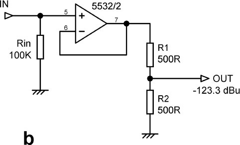
If we insist on an input impedance of 100 kΩ, how can we improve on our noise level of −108.2 dBu? The answer is by buffering the divider from the outside world. The output noise of a 5532 voltage-follower is about −119 dBu with a 50 Ω input termination. If this is used to drive our attenuator, the two resistors in it can be as low as the opamp can drive. The 5532 has a most convenient combination of low noise and good load-driving ability, and the divider resistors can be reduced to 500 Ω each, giving a load of 1 kΩ and a generous safety margin of drive capability. (Pushing the 5532 to its specified limit of a 500 Ω load tends to degrade its superb linearity by a small but measurable amount.) See Figure 1.9.
The noise from the resistive divider itself has now been lowered to −128.2 dBu, but there is of course the extra −119 dBu of noise from the voltage-follower that drives it. This however is halved by the divider just as the signal is, so the noise at the output will be the rms-sum of −125 dBu and −128.2 dBu, which is −123.3 dBu. A 6 dB attenuator is actually the worst case, as it has the highest possible source impedance for a given total divider resistance. Either more or less attenuation will mean less noise from the divider itself.
So, despite adding active circuitry that intrudes its own noise, the final noise level has been reduced from −108.2 to −123.3 dBu, an improvement of 15.1 dB.
How to Amplify Quietly
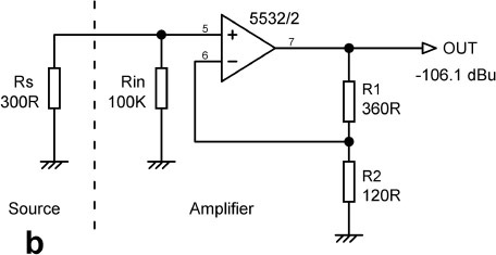
OK, we need a low-noise amplifier. Let’s assume we have a reasonably low source impedance of 300 Ω, and we need a gain of four times (+12 dB). Figure 1.10a shows a very ordinary circuit using half a 5532 with typical values of 3 kΩ and 1 kΩ in the feedback network, and the noise output measures as −105.0 dBu. The Johnson noise generated by the 300 Ω source resistance is −127.4 dBu, and amplifying that by a gain of four gives −115.4 dBu. Compare this with the actual −105.0 dBu we get, and the noise figure is 10.4 dB—in other words the noise from the amplifier is three times the inescapable noise from the source resistance, making the latter essentially negligible. This amplifier stage is clearly somewhat short of noise-free perfection, despite using one of the quieter opamps around.

We need to make things quieter. The obvious thing to do is to reduce the value of the feedback resistances; this will reduce their Johnson noise and also reduce the noise produced in them by the opamp current noise generators. Figure 1.10b shows the feedback network altered to 360 Ω and 120 Ω, adding up to a load of 480 Ω, pushing the limits of the lowest resistance the opamp can drive satisfactorily. This assumes of course that the next stage presents a relatively light load so that almost all of the driving capability can be used to drive the negative-feedback network; keeping tiny signals free from noise can involve throwing some serious current about. The noise output is reduced to −106.1 dBu, which is only an improvement of 1.1 dB and only brings the noise figure down to 9.3 dB, leaving us still a long way from what is theoretically attainable. However, at least it cost us nothing in extra components.
If we need to make things quieter yet, what can be done? The feedback resistances cannot be reduced further unless the opamp drive capability is increased in some way. An output stage made of discrete transistors could be added, but it would almost certainly compromise the low distortion we get from a 5532 alone. For one answer see the next section on ultra-low noise design.
How to Invert Quietly
Inverting a signal always requires the use of active electronics. (OK, you could use a transformer.) Assume that an input impedance of 47 kΩ is required, along with a unity-gain inversion. A straightforward inverting stage as shown in Figure 1.11a will give this input impedance and gain only if both resistors are 47 kΩ. These relatively high-value resistors contribute Johnson noise and exacerbate the effect of opamp current noise. Also the opamp is working at a noise gain of two times, so the noise output is high at −101.4 dBu.

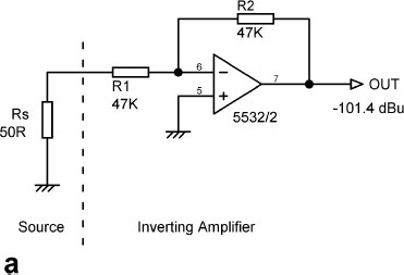

The only way to improve this noise level is to add another active stage. It sounds paradoxical—adding more nonsilent circuitry to reduce noise—but that’s the way the universe works. If a voltage-follower is added to the circuit give Figure 1.11b, then the resistors around the inverting opamp can be greatly reduced in value without reducing the input impedance, which can now be pretty much as high as we like. The “Noise buffered” column in Table 1.8 shows that if R1 and R2 are reduced to 2.2 kΩ the total noise output is lowered by 8.2 dB, which is a very useful improvement. If R1, R2 are further reduced to 1 kΩ, which is perfectly practical with a 5532’s drive capability, the total noise is reduced by 9.0 dB compared with the 47 kΩ case. The “Noise unbuffered” column gives the noise output with specified R value but without the buffer, demonstrating that adding the buffer does degrade the noise slightly, but the overall result is still far quieter than the unbuffered version with 47 kΩ resistors. In each case the circuit input is terminated to ground via 50 Ω.
How to Balance Quietly
The design of low-noise and ultra-low-noise balanced amplifiers using both low impedances and the multipath amplifier technology described here is examined in Chapter 4, “Preamp Architecture”.
Ultra-Low-Noise Design With Multipath Amplifiers
Are the circuit structures described earlier the ultimate? Is this as low as noise gets? No. In the search for low noise, a powerful technique is the use of parallel amplifiers with their outputs summed. This is especially useful where source impedances are low and therefore generate little noise compared with the voltage noise of the electronics.
R1, R2 value Ω |
Noise unbuffered |
Noise buffered |
Noise reduction dB Ref 47k case |
|---|---|---|---|
1 k |
−111.0 dBu |
−110.3 dBu |
9.0 |
2k2 |
−110.1 dBu |
−109.5 dBu |
8.2 |
4k7 |
−108.9 dBu |
−108.4 dBu |
7.1 |
10 k |
−106.9 dBu |
−106.6 dBu |
5.3 |
22 k |
−104.3 dBu |
−104.3 dBu |
3.0 |
47 k |
−101.4 dBu |
−101.3 dBu |
0 dB reference |
If there are two amplifiers connected, the signal gain increases by 6 dB due to the summation. The noise from the two amplifiers is also summed, but since the two noise sources are completely uncorrelated (coming from physically different components) they partially cancel, and the noise level only increases by 3 dB. Thus there is an improvement in signal-to-noise ratio of 3 dB. This strategy can be repeated by using four amplifiers, in which case the signal-to-noise improvement is 6 dB. Table 1.9 shows how this works for increasing numbers of amplifiers.
In practice the increased signal gain is not useful, and an active summing amplifier would compromise the noise improvement, so the output signals are averaged rather than summed, as shown in Figure 1.12. The amplifier outputs are simply connected together with low-value resistors, so the gain is unchanged but the noise output falls. The amplifier outputs are nominally identical, so very little current should flow from one opamp to another. The combining resistor values are so low that their Johnson noise can be ignored.
Obviously there are economic limits on how far you can take this sort of thing. Unless you’re measuring gravity waves or something equally important, 256 parallel amplifiers is probably not a viable choice.
Number of amplifiers |
Noise reduction |
|---|---|
1 |
0 dB ref |
2 |
−3.01 dB |
3 |
−4.77 dB |
4 |
−6.02 dB |
5 |
−6.99 dB |
6 |
−7.78 dB |
7 |
−8.45 dB |
8 |
−9.03 dB |
12 |
−10.79 dB |
16 |
−12.04 dB |
32 |
−15.05 dB |
64 |
−18.06 dB |
128 |
−21.07 dB |
256 |
−24.58 dB |
Be aware that this technique does not give any kind of fault redundancy. If one opamp turns up its toes, the low value of the averaging resistors means the whole stage will stop working.
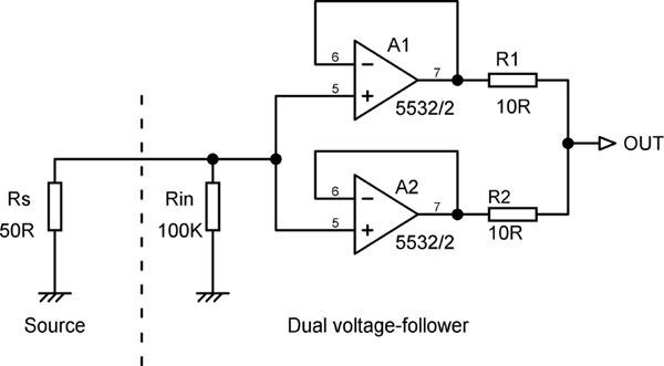
Ultra-Low-Noise Voltage Buffers
The multiple-path philosophy works well even with a minimally simple circuit such as a unity-gain voltage buffer. Table 1.10 gives calculated results for 5532 sections (the noise output is too low to measure reliably even with the best testgear) and shows how the noise output falls as more opamps are added. The distortion performance is not affected.
The 10 Ω output resistors combine the opamp outputs and limit the currents that would flow from output to output as a result of DC offset errors. AC gain errors here will be very small indeed because the opamps have 100% feedback. If the output resistors were raised to 47 Ω they would as usual give HF stability when driving screened cables or other capacitances, but the total output impedance is usefully halved to 23.5 Ω. Another interesting bonus of this technique is that we have doubled the output drive capability; this stage can easily drive 300 Ω. This can be very useful when using low- impedance design to reduce noise in the following stage.
Number of opamps |
Calculated noise out |
|---|---|
1 |
−120.4 dBu |
2 |
−123.4 dBu |
3 |
−125.2 dBu |
4 |
−126.4 dBu |
Ultra-Low-Noise Amplifiers
We now return to the problem studied earlier; how to make a really quiet amplifier with a gain of four times. We saw that the minimum noise output using a single 5532 section and a 300 Ω source resistance was −106.1 dBu, with a not particularly impressive noise figure of 9.3 dB. Since almost all the noise is being generated in the amplifier rather than the source resistance, the multiple-path technique should work well here. And it does.
There is, however, a potential snag that needs to be considered. In the previous section we were combining the outputs of voltage followers, which have gains very close indeed to unity because they have 100% negative feedback and no resistors are involved in setting the gain. We could be confident that the output signals would be near-identical and unwanted currents flowing from one opamp to the other would be small despite the low value of the combining resistors.
The situation here is different; the amplifiers have a gain of four times, so there is a smaller negative feedback factor to stabilise the gain, and there are two resistors with tolerances that set the closed-loop gain for each stage. We need to keep the combining resistors low to minimise their Johnson noise, so things might get awkward. It seems reasonable to assume that the feedback resistors will be 1% components. Considering the two-amplifier configuration in Figure 1.13, the worst case would be to have R1a 1% high and R2a 1% low in one amplifier, while the other had the opposite condition of R1b 1% low and R2b 1% high. This highly unlikely state of affairs gives a gain of 4.06 times in the first amplifier and 3.94 times in the second. Making the further assumption of a 10 Vrms maximum voltage swing, we get 10.15 Vrms at the first output and 9.85 Vrms at the second, both applied to the combining resistors, which here are set at 47 Ω. The maximum possible current flowing from one amplifier output into the other is therefore 0.3V/(47 Ω + 47 Ω) which is 3.2 mA; in practice it will be much smaller. There are no problems with linearity or headroom, and distortion performance is indistinguishable from that of a single opamp.
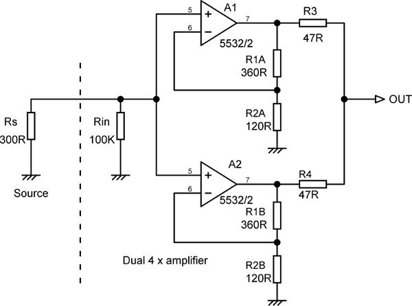
Having reassured ourselves on this point, we can examine the circuit of Figure 1.13, with two amplifiers combining their outputs. This reduces the noise at the output by 2.2 dB. This falls short of the 3 dB improvement we might hope for because of a significant Johnson noise contribution from source resistance, and doubling the number of amplifier stages again only achieves another 1.3 dB improvement. The improvement is greater with lower source resistances; the measured results with 1, 2, 3, and 4 opamps for three different source resistances are summarised in Table 1.11.
Rs Ω |
No of opamps |
Noise out |
Improvement |
|---|---|---|---|
300 |
1 |
−106.1 dBu |
0 dB ref |
300 |
2 |
−108.2 dBu |
2.2 dB |
300 |
3 |
−109.0 dBu |
2.9 dB |
300 |
4 |
−109.6 dBu |
3.5 dB |
200 |
1 |
−106.2 dBu |
0 dB ref |
200 |
2 |
−108.4 dBu |
2.2 dB |
200 |
3 |
−109.3 dBu |
3.1 dB |
200 |
4 |
−110.0 dBu |
3.8 dB |
100 |
1 |
−106.3 dBu |
0 dB ref |
100 |
2 |
−108.7 dBu |
2.4 dB |
100 |
3 |
−109.8 dBu |
3.5 dB |
100 |
4 |
−110.4 dBu |
3.9 dB |
The results for 200 Ω and 100 Ω show that the improvement with multiple amplifiers is greater for lower source resistances, as these resistances generate less Johnson noise of their own.
Multiple Amplifiers for Greater Drive Capability
We have just seen that the use of multiple amplifiers with averaged outputs not only reduces noise but increases the drive capability proportionally to the number of amplifiers employed. This is highly convenient because heavy loads need to be driven when pushing hard the technique of low-impedance design.
Using multiple amplifiers gets difficult when the stage has variable feedback to implement gain control or tone control. In this case the configuration in Figure 1.14 doubles the drive capability in a foolproof manner; I have always called it “mother’s little helper”. A1 may be enmeshed in as complicated a circuit as you like, but unity-gain buffer A2 will robustly carry it its humble duty of sharing the load. This is unlikely to give any noise advantage, as most of the noise will presumably come from the more complex circuitry around A1.

It is assumed that A1 has load-driving capabilities equivalent to those of A2. This approach is more parts-efficient than simply putting a multiple-buffer like that in Figure 1.11 after A1; that would make no use of the drive capability of A1. This technique was used to drive the input of a Baxandall volume control using 1 kΩ pots in the Elektor 2012 preamplifier design.[13]
An interesting point is that any extra distortion contribution from A2 is halved, because its output is averaged with the input signal from A1. Likewise the noise contribution of A2 is halved. Quite a help, really.
References
1. Smith, J. Modern Operational Circuit Design. Wiley-Interscience, 1971, p. 129.
2. Intersil Application Note AN9420.1. Current Feedback Amplifier Theory and Applications. Apr 1995.
3. Self, D. Audio Power Amplifier Design. 6th Edition. Focal Press, 2013, Chapter 3. ISBN 978-0-240-52613-3.
4. Self, D. “The 5532 OpAmplifier” Elektor, Oct and Nov 2010.
5. Wikipedia https://en.wikipedia.org/wiki/White_noise Accessed Nov 2016.
6. Wikipedia https://en.wikipedia.org/wiki/Pink_noise Accessed Nov 2016.
7. Wikipedia https://en.wikipedia.org/wiki/Brownian_noise Accessed Nov 2016.
8. Yellott, J. I. Jr. “Spectral Consequences of Photoreceptor Sampling in the Rhesus Retina” Science, Volume 221, 1983, pp. 382–385.
9. Johnson, J. “Thermal Agitation of Electricity in Conductors” Physical Review, Volume 32, 1928, p. 97.
10. Chong, Z. Y., and Sansen, W. Low-Noise Wideband Amplifiers in Bipolar & CMOS Technologies. Kluwer, 1991, p. 106.
11. de Gevel van, M. “Gramophone Preamplifier Noise Calculations—the 3852 Hz Rule Revisited” Linear Audio, Volume 8, Sept 2014, p. 129.
12. Groner, S. “A Low-Noise Laboratory-Grade Measurement Preamplifier” Linear Audio, Volume 3, Apr 2012, p. 143. ISBN 978-9490929-008.
13. Self, D. “Preamplifier 2012” Elektor, Apr, May, June 2012.