
Chapter 14
Line Outputs
Unbalanced Outputs
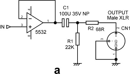
There are only two electrical output terminals for an unbalanced output—signal and ground. However, the unbalanced output stage in Figure 14.1a is fitted with a three-pin XLR connector to emphasise that it is always possible to connect the cold wire in a balanced cable to the ground at the output end and still get all the benefits of common-mode rejection if you have a balanced input. If a two-terminal connector is fitted, the link between the cold wire and ground has to be made inside the connector.
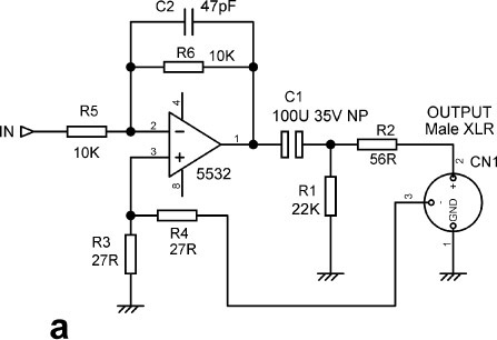
The output amplifier in Figure 14.1a is configured as a unity-gain buffer, though in some cases it will be connected as a series-feedback amplifier to give gain. A non-polarised DC-blocking capacitor C1 is included; 100 uF gives a −3 dB point of 2.6 Hz with one of those notional 600 Ω loads. The opamp is isolated from the line shunt capacitance by a resistor R2, in the range 47–100 Ω, to ensure HF stability, and this unbalances the hot and cold line impedances. A drain resistor R1 ensures that no charge can be left on the output side of C1; it is placed before R2, so it causes no attenuation. In this case the loss would only be 0.03 dB, but such errors can build up to an irritating level in a large system, and it costs nothing to avoid them.
If the cold line is simply grounded as in Figure 14.1a, then the presence of R2 degrades the CMRR of the interconnection to an uninspiring −43 dB even if the balanced input at the other end of the cable has infinite CMRR in itself and perfectly matched 10 kΩ input impedances.
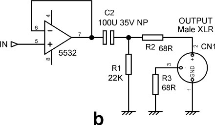
To fix this problem, Figure 14.1b shows what is called an impedance-balanced output. There are now three physical terminals, hot, cold, and ground. The cold terminal is neither an input nor an output but a resistive termination R3 with the same resistance as the hot terminal output impedance R2. If an unbalanced input is being driven, this cold terminal can be either shorted to ground locally or left open circuit. The use of the word “balanced” is perhaps unfortunate, as when taken together with an XLR output connector it implies a true balanced output with anti-phase outputs, which is not what you are getting. The impedance-balanced approach is not particularly cost-effective, as it requires significant extra money to be spent on an XLR connector. Adding an opamp inverter to make it a proper balanced output costs little more, especially if there happens to be a spare opamp half available, and it sounds much better in the specification.
Zero-impedance Outputs
Both the unbalanced outputs shown in Figure 14.1 have series output resistors to ensure stability when driving cable capacitance. This increases the output impedance, which can impair the CMRR of a balanced interconnection and can also lead to increased crosstalk via stray capacitance in some situations. One such scenario that was authoritatively fixed by the use of a so-called “zero-impedance” output is described in my book Small Signal Audio Design in Chapter 22 in the section on mixer insert points.[1] The output impedance is of course not exactly zero, but it is very low compared with the average series output resistor.
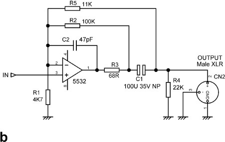
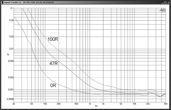
Figure 14.2a shows how the zero-impedance technique is applied to an unbalanced output stage with 10 dB of gain. Feedback at audio frequencies is taken from outside isolating resistor R3 via R2, while the HF feedback is taken from inside R3 via C2, so it is not affected by load capacitance and stability is unimpaired. Using a 5532 opamp, the output impedance is reduced from 68 ohms to 0.24 ohms at 1 kHz—a dramatic reduction that would reduce capacitive crosstalk by 49 dB. Output impedance increases to 2.4 Ohms at 10 kHz and 4.8 Ohms at 20 kHz, as opamp open-loop gain falls with frequency. The impedance-balancing resistor on the cold pin has been replaced by a link to match the near-zero output impedance at the hot pin. More details on zero-impedance outputs are given later in this chapter in the section on balanced outputs.
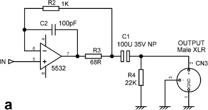

There is no need for the output stage to have voltage gain for this to work, just a way to transfer the negative feedback point from outside to inside the series output resistor. Figure 14.3a shows a version using a unity-gain voltage-follower.
The quickest way to measure normal output impedances is to load each output as heavily as is practical (say with 560 Ω) and measure the voltage drop compared with the unloaded state. From this the output impedance is simply calculated. However, in the case of zero-impedance outputs the voltage drop is very small, and so measurement accuracy is poor.
A more sophisticated technique is the injection of a test signal current into the output and measuring the voltage that results. This is much more informative; the results for the hot output in Figure 14.3a are given in Figure 14.4. A suitable current to inject is 1 mA rms, defined by applying 1 Vrms to a 1 kΩ injection resistor. A 1 Ω output impedance will therefore give an output signal voltage of 1 mV rms (−60 dBV), which can be easily measured, as in Figure 14.4. Likewise, −40 dBV represents 10 Ω, and −80 dBV represents 0.1 Ω; a log scale is useful because it allows a wide range of impedance to be displayed and gives convenient straight lines on the plot. The opamp sections were both LM4562.
Below 3 kHz the impedance increases steadily as frequency falls, doubling with each octave due to the reactance of the output capacitor. This effect can be reduced simply by increasing the size of the capacitor. In Figure 14.4 the results are shown for 220uF, 470uF, and 1000uF output capacitors. For 1000uF a broad null occurs, reaching down to 0.06 Ω, and the output impedance is below 1 Ω between 150 Hz and 20 kHz. Bear in mind that output capacitors should be nonpolarised types, as they may face external DC voltages of either polarity and should be rated at no less than 35 V; this means that a 1000 uF capacitor can be quite a large component.
In Figure 14.4 the modulus of the output impedance falls to below 0.1 Ω between 1 and 5 kHz. It is easy to assume that the steady rise above the latter frequency is due to the open-loop gain of the opamp falling as frequency increases, and indeed I did, until recently. However, an apparent anomaly in some measured results (it was Isaac Asimov who said that most scientific advances start with “hmmm … that’s funny …” rather than “Eureka!”), where a two-times change in noise gain (see the balanced output section later in this chapter) gave identical output impedance plots, led me to dig a little deeper.

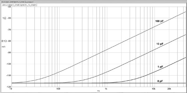
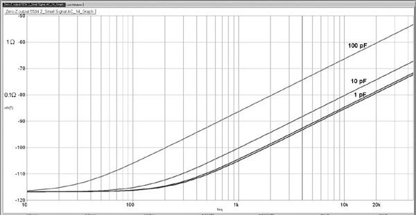
Figure 14.5 shows the output impedance with the output blocking capacitor removed; R2 is 1 kΩ.
I’m not entirely sure that the line at the bottom for no C at all should be dead flat, but at any rate the point is illustrated.
Figure 14.6 shows the effect of adding a 10 pF capacitor across the external compensation pins of the 5534. Now the 0 pF and 1 pF curves are close to that for 10 pF, but the 100 pF curve stays where it was and is still ten times higher. When this simulation is repeated using a TL072 (which has less open-loop gain in the HF region) the curves are much closer together and the 100 pF passes through −60 dB at 10 kHz instead of −68 dB, so here the HF open-loop gain of the opamp really does define the situation. Historically many output amplifiers were built with TL072s, due to the higher cost and power consumption of the 5534/2, but the values used were frequently R2 = 10 kΩ and C2 = 100 pF, so then the transition frequency between the feedback paths was still the defining factor for the HF output impedance.
The voltage-follower in Figure 14.3a is known to be stable with R2 = 1k and C2 = 100 pF; this gives an output impedance of 10 Ω at 20 kHz. While making C2 = 10 pF gives a useful reduction to 0.2 Ω, its stability needs to be checked. We will use 100 pF from here on.
We will now put back the output blocking capacitor and examine the output impedance at the low-frequency end. The situation is simpler at LF because the components are of known value (apart from the usual manufacturing tolerances) and performance is not significantly affected by variable opamp parameters.
Figure 14.7 shows the radical effect; the LF output impedance is now much higher and, as expected, doubles for every halving of frequency. The middle trace is for an output capacitor of 470 uF, which for size reasons (as a nonpolarised electrolytic it is larger than the usual polarised sort) is probably the highest value you would want to use in practice; note how accurately it matches the measured impedance result for 470 uF in Figure 14.4. The 5534 is now uncompensated, as it gives a better match of HF open-loop gain with the 5532s or LM4562s that will be used in practice
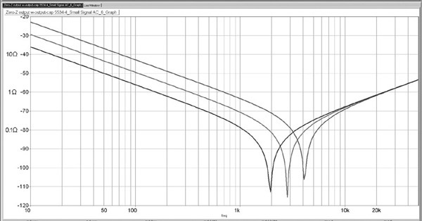
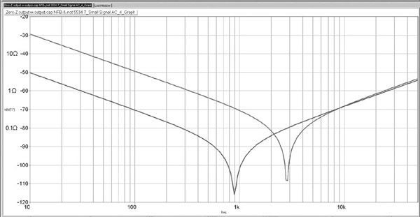
The voltage at 50 Hz, the lowest frequency of interest, is −44 dB, equivalent to an output impedance of 6.3 Ω, which is much higher than the impedance set by the opamp and some way distant from “zero impedance”. We can use a 1000 uF output capacitor instead, which reduces the output impedance at 50 Hz to 3.1 Ω, but the capacitor is now distinctly bulky. From here on we will stick with 470 uF.
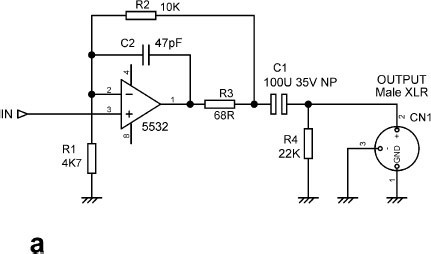
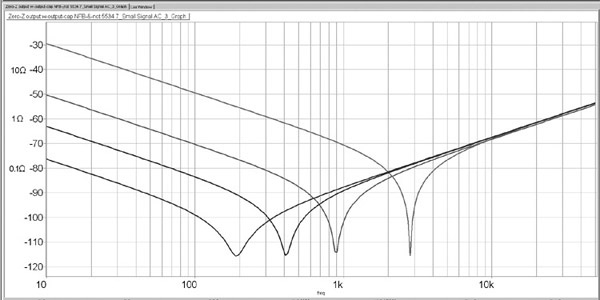
What do we do now if we want a lower LF output impedance? As is so often the case, in electronics as in life, you can use either brawn (big capacitors) or brains. The latter, once again as is so often true, is the cunning application of negative feedback. The essence of the zero impedance technique is to have two NFB paths, with one enclosing the output resistor, which could be called double feedback. If we add a third NFB path, as in Figure 14.3b, then we can enclose the output capacitor as well and reduce the effects of its reactance; we’ll call this triple feedback. Figure 14.8 shows the dramatic results. The output impedance at 50 Hz drops from 6.3 Ω to 0.63 Ω, which has a much better claim to be “zero impedance”. This ten-fold improvement continues up to about 400 Hz, where the triple-feedback output impedance plummets into a cancellation crevasse. We still get a useful reduction up to 2 kHz, but above that the double-feedback circuit has its own crevasse. As expected, the output impedances at HF are the same.
Figure 14.3b shows the outer NFB path R5 as 1 kΩ and the middle path R2 as 10 kΩ, chosen on the grounds that the outer path has to overpower the middle path at low frequencies. There is the snag that the output is no longer DC blocked. The value of R2 has a powerful effect on the output impedance, as illustrated in Figure 14.9.
The triple-feedback method has another advantage; it radically extends the frequency response, as it effectively multiplies the value of the output capacitor. A 470 uF output capacitor with a 600 Ω load (a largely fictitious worst case) has a −3 dB roll-off at 0.58 Hz; this is what we get with double feedback. The roll-off frequency is deliberately made very low to avoid capacitor distortion (see Chapter 3).
With triple feedback as in Figure 14.3b, the −3 dB point drops to 0.035 Hz, which is lower than we need or want. This leads to the interesting speculation that we could reduce the output capacitor to 47 uF and still get satisfactory results for frequency response. I haven’t tried this, and I am not sure what would happen with the capacitor distortion issue.
Since wiring resistances internal to the equipment are likely to be in the region 0.1 to 0.5 Ω, there seems nothing much to be gained by reducing the output impedances any further than is achieved by this simple zero-impedance technique.
You may be thinking that the zero-impedance output is a bit of a risky business; will it always be stable when loaded with capacitance? In my wide experience of this technique, the answer is yes, so long as you design it properly. If you are attempting something different from proven circuitry, it is always wise to check the stability of zero-impedance outputs with a variety of load capacitances. In the example of Figure 14.3, both versions were separately checked using a 5 Vrms sweep from 50 kHz to 10 Hz, with load capacitances of 470 pF, 1 nF, 2n2, 10 nF, 22 nF and 100 nF. At no point was there the slightest hint of instability. A load of 100 nF is of course grossly excessive compared with real use, being equivalent to about 1000 metres of average screened cable, and curtails the output swing at HF due to opamp current-limiting.
Figure 14.3b with its triple feedback paths has another advantage. In Chapter 2 we saw how electrolytic coupling capacitors can introduce distortion even if the time-constant is long enough to give a flat LF response. In Figure 14.3b most of the feedback is now taken from outside C1, via R5, so it can correct capacitor distortion. The DC feedback goes via R2, now much higher in value, and the HF feedback goes through C2 as before to maintain stability with capacitive loads. R2 and R5 in parallel come to 10 kΩ, so the gain is the same. Any circuit with separate DC and AC feedback paths must be checked carefully for frequency response irregularities, which may happen well below 10 Hz. A function generator is useful for this.
Ground-Cancelling Outputs: Basics
This technique, also called a ground-compensated output, appeared in the early 1980s in mixing consoles. It allows ground voltages to be cancelled out even if the receiving equipment has an unbalanced input; it prevents any possibility of creating a phase error by miswiring; and it costs virtually nothing except for the provision of a three-pin output connector.
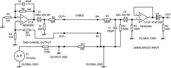
Ground-cancelling (GC) separates the wanted signal from the unwanted ground voltage by addition at the output end of the link rather than by subtraction at the input end. If the receiving equipment ground differs in voltage from the sending ground, then this difference is added to the output signal so that the signal reaching the receiving equipment has the same ground voltage superimposed upon it. Input and ground therefore move together, and the ground voltage has no effect, subject to the usual effects of component tolerances. The connecting lead is differently wired from the more common unbalanced-out balanced-in situation, as now the cold line is be joined to ground at the input or receiving end. This is illustrated in Figure 14.10, which compares a conventional balanced link with a GC link.

An inverting unity-gain ground-cancel output stage is shown in Figure 14.11a. The cold pin of the output socket is now an input and has a unity-gain path summing into the main signal going to the hot output pin to add the ground voltage. This path R3, R4 has a very low input impedance equal to the hot terminal output impedance, so if it is used with a balanced input, the line impedances will be balanced and the combination will still work effectively. The 6dB of attenuation in the R3-R4 divider is undone by the gain of two set by R5, R6. It is unfamiliar to most people to have the cold pin of an output socket as a low-impedance input, and its very low input impedance minimises the problems caused by miswiring. Shorting it locally to ground merely converts the output to a standard unbalanced type. On the other hand, if the cold input is left unconnected then there will be a negligible increase in noise due to the very low resistance of R3.

This is the most economical GC output and is very useful to follow an inverting stage, as it corrects the phase. However, a phase inversion is not always convenient, and Figure 14.11b shows a noninverting GC output stage with a gain of 6.6 dB. R5 and R6 set up a gain of 9.9 dB for the amplifier, but the overall gain is reduced by 3.3 dB by attenuator R3, R4. The cold line is now terminated by R7, and any signal coming in via the cold pin is attenuated by R3, R4 and summed at unity gain with the input signal. The stage must be fed from a very low impedance, such as an opamp output, for the summation to be accurate and thus the ground-cancelling to work properly. There is a slight compromise on noise performance here because attenuation is followed by amplification.
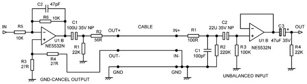
Figure 14.12 shows the complete circuit of a GC link using an inverting ground-cancel output stage. EMC filtering and DC blocking are included for the unbalanced input stage.
Ground-Cancelling Outputs: CMRR
In a balanced link, the CMRR is a measure of how accurately the subtraction is performed at the receiving end and so of how effectively ground noise is nulled. A GC link also has an equivalent CMRR that measures how accurately the addition is performed at the sending end. Figure 14.13 shows (for the first time, I think) how to measure the CMRR of a ground-cancelling link. It is slightly more complicated than for the balanced case.
In Figure 14.13, a 10 Ω resistor R17 is inserted into the ground of the interconnection. This allows the signal generator V1 to move the output ground of the sending amplifier up and down with respect to the global ground, via R18. Quite a lot of power has to be supplied so that R17 can be kept low in value. Normally the input to the GC output stage is via R5; for this test the input is grounded, as shown. If the send amplifier is working properly, the signal applied to OUT will cancel the signal on the output ground, so that as far as the input of the receiving amplifier is concerned, it does not exist. Be clear that here we are measuring the CMRR of the sending amplifier, not the receiving amplifier.
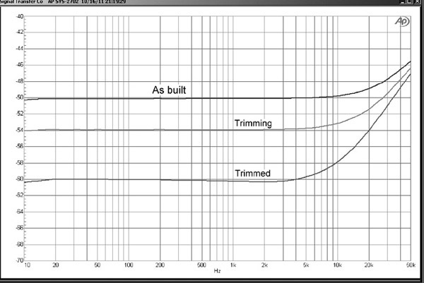
Just as the CMRR of a balanced link depends on the accuracy of the resistors and the open-loop gain of the opamp in the receiving amplifier, the same parameters determine the CMRR of a ground-cancel send amplifier. The measured results from the arrangement in Figure 14.13 are given in Figure 14.14; the CMRR as built (with 1% resistors) was −50 dB, flat up to 10 kHz. The two lower traces were obtained by progressively trimming the value of R6 to minimise the output. If high CMRR is required a preset adjustment can be used, just as in balanced line input amplifiers.
Ground-cancelling outputs are an economical way of making ground loops innocuous when there is no balanced input, and it is rather surprising they are not more popular; perhaps it is because people find the notion of an input pin on an output connector unsettling. In particular GC outputs would appear to offer the possibility of a quieter interconnection than the standard balanced interconnection because a relatively noisy balanced input is not required. Ground-cancelling outputs can also be made zero impedance using the techniques described earlier.
Ground-Cancelling Outputs: Send Amplifier Noise
In Figures 14.12 and 14.13, the gain-setting resistors R5 and R6 have the relatively high value of 10 kΩ, for comparison with the “standard” balanced input amplifier made with four 10 kΩ resistors. Reducing their value in accordance with the principles of low-impedance design gives useful reductions in noise, as shown by the measurements in Table 14.1. A 5532 opamp was used.
A very useful 4.3 dB reduction in noise is gained by reducing R5 and R6 to 2k2, at zero cost, but after that the improvements become smaller, for while Johnson noise and the effects of current noise are reduced, the voltage noise of the opamp is unchanged.
It is instructive to compare the signal/noise ratio with that of a balanced link. We will put 1 Vrms (+2.2 dBu) down a balanced link. The balanced output stage raises the level by 6 dB, so we have +8.2 dBu going down the cable. A conventional unity-gain balanced input made with 10 kΩ resistors and a 5532 section has a noise output of −104.8 dBu, so the signal/noise ratio is 8.2 + 104.8 = −113.0 dB.
In the ground-cancel case, if we use 1 kΩ resistors as in the third row of Table 14.1, the noise from the ground-cancel output stage is −112.2 dBu. Adding the noise of the 5532 buffer at the receiving end in Figure 14.12, which is −125.7 dBu, we get −112.0 dBu as the noise floor. The signal/noise ratio is therefore 2.2 + 112.0 = −114.2 dB. This is 1.2 dB quieter than the conventional balanced link, and it only uses two opamp sections instead of three.
Value of R5, R6 |
Noise output |
Improvement |
|---|---|---|
10 kΩ |
−107.2 dBu |
0.0 dB |
2k2 |
−111.3 dBu |
−4.3 dB |
1 kΩ |
−112.2 dBu |
−5.0 dB |
560 Ω |
−112.6 dBu |
−5.4 dB |
The noise situation could easily be reversed by using a low-impedance balanced input with buffers to make the input impedance acceptably high, as described in Small Signal Audio Design,[2] but we are then comparing a ground-cancel link using two opamp sections with a balanced link using four of them.
Balanced Outputs: Basics
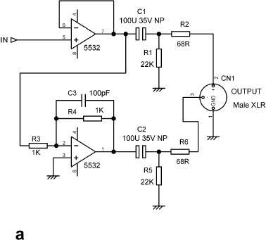
Figure 14.15a shows a balanced output, where the cold terminal carries the same signal as the hot terminal but phase-inverted. This can be arranged simply by using an opamp stage to invert the normal in-phase output. The resistors R3, R4 around the inverter should be as low in value as possible to minimise Johnson and input-current noise, because this stage is working at a noise gain of two, but bear in mind that R3 is effectively grounded at one end, and its loading, as well as the external load, must be driven by the first opamp. A unity-gain follower is shown for the first amplifier, but this can be any other shunt or series-feedback stage, as convenient. The inverting output if not required can be ignored; it must not be grounded, because the inverting opamp will then spend most of its time clipping in current-limiting, probably injecting unpleasant distortion into the grounding system. Both hot and cold outputs must have the same output impedances (R2, R6) to keep the line impedances balanced and the interconnection CMRR maximised.
A balanced output has the advantage that the total signal level on the line is increased by 6 dB, which will improve the signal-to-noise ratio if a balanced input amplifier is being driven, as they are relatively noisy. It is also less likely to crosstalk to other lines even if they are unbalanced, as the currents injected via the stray capacitance from each line will tend to cancel; how well this works depends on the physical layout of the conductors. All balanced outputs give the facility of correcting phase errors by swapping hot and cold outputs. This is however a two-edged sword, because it is probably how the phase got wrong in the first place.
There is no need to worry about the exact symmetry of level for the two output signals; ordinary tolerance resistors are fine. Such gain errors only affect the signal-handling capacity of the interconnection by a small amount. This simple form of balanced output is the norm in hi-fi balanced interconnection but is less common in professional audio, where the quasi-floating output described here gives more flexibility.
Balanced Outputs: Output Impedance
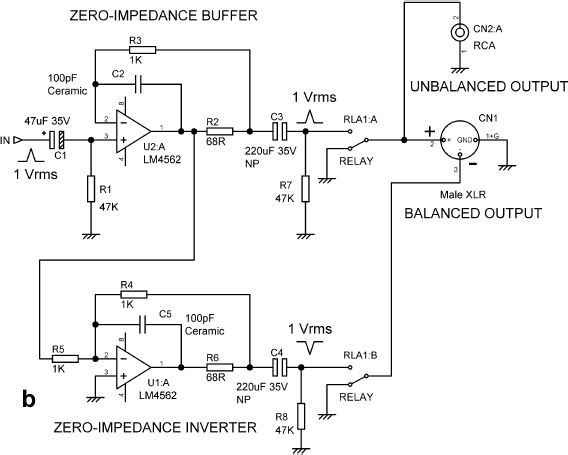
The balanced output stage of Figure 14.15a has an output impedance of 68 Ω on both legs because this is the value of the series output resistors; however, as noted earlier, the lower the output impedance the better, so long as stability is maintained. This balanced output configuration can be easily adapted to have two zero- impedance outputs, as shown in Figure 14.15b. The unity- gain buffer that drives the hot output is as described earlier. The zero-impedance inverter that drives the cold output works similarly, but with shunt negative feedback via R4.
The output impedance plot for the cold output was identical to Figure 14.4. This came as rather a surprise because the inverter works at a noise gain of two times, as opposed to the buffer, which works at a noise gain of unity, and so I expected it to show twice the output impedance above 5 kHz. This observation prompted me to investigate the effect of the feedback capacitor value, as described earlier.
Balanced Outputs: Noise
The noise output of the zero-impedance balanced output of Figure 14.15b was measured with 0 Ω source resistance, rms response, unweighted and measured at two bandwidths to demonstrate the absence of hum; the opamp sections were both LM4562. See Table 14.2.
Table 14.2 shows that reading the noise between the hot and cold outputs gives results 3 dB higher. This does not mean balanced operation is inferior; the total signal level is twice as high, and so the signal-to-noise ratio is in fact 3 dB better. This calculation does not take account of the noise added at the receiving amplifier end of a balanced link.
Transformer Balanced Outputs
If true galvanic isolation between equipment grounds is required, this can only be achieved with a line transformer, sometimes called a line isolating transformer. You don’t use line transformers unless you really have to because the much-discussed cost, weight, and performance problems are very real, as you will see shortly. However they are sometimes found in big sound reinforcement systems (for example in the mic-splitter box on the stage) and in any environment where high RF field strengths are encountered.
Output |
Noise out |
Bandwidth |
|---|---|---|
Hot output only |
−113.5 dBu |
(22–22 kHz) |
Hot output only |
−113.8 dBu |
(400–22 kHz) |
Balanced output (hot & cold) |
−110.2 dBu |
(22–22 kHz) |
Balanced output (hot & cold) |
−110.5 dBu |
(400–22 kHz) |
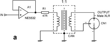
A basic transformer balanced output is shown in Figure 14.16a; in practice A1 would probably be providing gain rather than just buffering. In good-quality line transformers there will be an inter-winding screen, which should be earthed to minimise noise pickup and general EMC problems. In most cases this does not ground the external can, and you have to arrange this yourself, possibly by mounting the can in a metal capacitor clip. Make sure the can is grounded, as this definitely does reduce noise pickup.
Be aware that the output impedance will be higher than usual because of the ohmic resistance of the transformer windings. With a 1:1 transformer, as normally used, both the primary and secondary winding resistances are effectively in series with the output. A small line transformer can easily have 60 Ω per winding, so the output impedance is 120 Ω plus the value of the series resistance R1 added to the primary circuit to prevent HF instability due to transformer winding capacitances and line capacitances. The total can easily be 160 Ω or more, compared with, say, 47 Ω for nontransformer output stages. This will mean a higher output impedance and greater voltage losses when driving heavy loads.
DC flowing through the primary winding of a transformer is bad for linearity, and if your opamp output has anything more than the usual small offset voltages on it, DC current flow should be stopped by a blocking capacitor.
Output Transformer Frequency Response
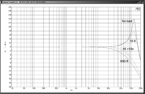
Line input transformers give a nastily peaking high- frequency response if the secondary is not loaded properly, due to resonance between the leakage inductance and the stray winding capacitances. Exactly the same problem afflicts output transformers, as shown in Figure 14.17; with no output loading there is a frightening 14 dB peak at 127 kHz. This is high enough in frequency to have very little effect on the response at 20 kHz, but this high-Q resonance isn’t the sort of horror you want lurking in your circuitry. It could easily cause some nasty EMC problems.
The transformer measured was a Sowter 3292 1:1 line isolating transformer. Sowter are a highly respected company, and this is a quality part with a mumetal core and housed in a mumetal can for magnetic shielding. When used as the manufacturer intended, with a 600 Ω load on the secondary, the results are predictably quite different, with a well-controlled roll-off that I measured as −0.5 dB at 20 kHz.
The difficulty is that there are very few if any genuine 600 Ω loads left in the world, and most output transformers are going to be driving much higher impedances. If we are driving a 10 kΩ load, the secondary resonance is not much damped, and we still get a thoroughly unwelcome 7 dB peak above 100 kHz, as shown in Figure 14.17. We could of course put a permanent 600 Ω load across the secondary, but that will heavily load the output opamp, impairing its linearity, and will give us unwelcome signal loss due in the winding resistances. It is also a profoundly inelegant way of carrying on.
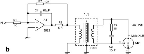
A better answer, as in the case of the line input transformer, is to put a Zobel network, i.e. a series combination of resistor and capacitor, across the secondary, as in Figure 14.16b. The capacitor required is quite small and will cause very little loading except at high frequencies, where signal amplitudes are low. A little experimentation yielded the values of 1 kΩ in series with 15 nF, which gives the much improved response shown in Figure 14.17. The response is almost exactly 0.0 dB at 20 kHz, at the cost of a very gentle 0.1 dB rise around 10 kHz; this could probably be improved by a little more tweaking of the Zobel values. Be aware that a different transformer type will require different values.
Output Transformer Distortion
Transformers have well-known problems with linearity at low frequencies. This is because the voltage induced into the secondary winding depends on the rate of change of the magnetic field in the core, and so the lower the frequency, the greater the change in magnetic flux must be for transformer action.[3] The current drawn by the primary winding to establish this field is nonlinear because of the well-known nonlinearity of iron cores. If the primary had zero resistance and was fed from a zero source impedance, as much distorted current as was needed would be drawn, and no one would ever know there was a problem. But … there is always some primary resistance, and this alters the primary current drawn so that third-harmonic distortion is introduced into the magnetic field established and so into the secondary output voltage. Very often there is a series resistance R1 deliberately inserted into the primary circuit, with the intention of avoiding HF instability; this makes the LF distortion problem worse, and a better means of isolation is a low-value inductor of say 4 uH in parallel with a low-value damping resistor of around 47 Ω. This is more expensive and is only used on high-end consoles.
An important point is that this distortion does not appear only with heavy loading—it is there all the time, even with no load at all on the secondary; it is not analogous to loading the output of a solid-state power amplifier, which invariably increases the distortion. In fact, in my experience transformer LF distortion is slightly better when the secondary is connected to its rated load resistance. With no secondary load, the transformer appears as a big inductance, so as frequency falls the current drawn increases, until, with circuits like Figure 14.11a, there is a sudden steep increase in distortion around 10–20 Hz as the opamp hits its output current limits. Before this happens, the distortion from the transformer itself will be gross.
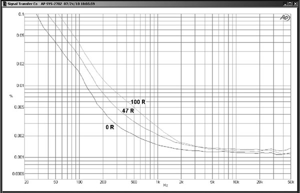
To demonstrate this I did some distortion tests on the same Sowter 3292 transformer that was examined for frequency response. The winding resistance for both primary and secondary is about 59 Ω. It is quite a small component, 34 mm in diameter and 24 mm high and weighing 45 gm, and is obviously not intended for transferring large amounts of power at low frequencies. Figure 14.18 shows the LF distortion with no series resistance, driven directly from a 5532 output, (there were no HF stability problems in this case, but it might be different with cables connected to the secondary) and with 47 and 100 Ω added in series with the primary. The flat part to the right is the noise floor.
Taking 200 Hz as an example, adding 47 Ω in series increases the THD from 0.0045% to 0.0080%, figures which are in exactly the same ratio as the total resistances in the primary circuit in the two cases. It’s very satisfying when a piece of theory slots right home like that. Predictably, a 100 Ω series resistor gives even more distortion, namely 0.013 % at 200 Hz, and once more proportional to the total primary resistance.
If you’re used to the near-zero LF distortion of opamps, you may not be too impressed with Figure 14.18, but this is the reality of output transformers. The results are well within the manufacturer’s specifications for a high-quality part. Note that the distortion rises rapidly to the LF end, roughly tripling as frequency halves. It also increases fast with level, roughly quadrupling as level doubles. Having gone to some pains to make electronics with very low distortion, this nonlinearity at the very end of the signal chain is distinctly irritating. The situation is somewhat eased in actual use, as signal levels in the bottom octave of audio are normally about 10–12 dB lower than the maximum amplitudes at higher frequencies.
Reducing Output Transformer Distortion
In audio electronics, as in so many other areas of life, there is often a choice between using brains or brawn to tackle a problem. In this case “brawn” means a bigger transformer, such as the Sowter 3991, which is still 34 mm in diameter but 37 mm high, weighing in at 80 gm. The extra mumetal core material improves the LF performance, but you still get a distortion plot very much like Figure 14.18, (with the same increase of THD with series resistance), except now it occurs at 2 Vrms instead of 1 Vrms. Twice the metal, twice the level—I suppose it makes sense. You can take this approach a good deal further with the Sowter 4231, a much bigger open-frame design tipping the scales at a hefty 350 gm. The winding resistance for the primary is 12 Ω and for the secondary 13.3 Ω, both a good deal lower than the previous figures.
Figure 14.19 shows the LF distortion for the Sowter 4231 with no series resistance and with 47 and 100 Ω added in series with the primary. The flat part to the right is the noise floor. Comparing it with Figure 14.13 the basic distortion at 30 Hz is now 0.015%, compared with about 0.10% for the 3292 transformer. While this is a useful improvement it is gained at considerable expense. Now adding 47 Ω of series resistance has dreadful results—distortion increases by about five times. This is because the lower winding resistances of the 4231 mean that the added 47 Ω has increased the total resistance in the primary circuit to five times what it was. Predictably, adding a 100 Ω series resistance approximately doubles the distortion again. In general bigger transformers have thicker wire in the windings, and this in itself reduces the effect of the basic core nonlinearity, quite apart from the improvement due to more core material. A lower winding resistance also means a lower output impedance.
The LF nonlinearity in Figure 14.19 is still most unsatisfactory compared with that of the electronics. Since the “My policy is copper and iron!”[4] approach does not really solve the problem, we’d better put brawn to one side and try what brains we can muster.
We have seen that adding series resistance to ensure HF stability makes things definitely worse, and a better means of isolation is a low-value inductor of say 4 uH paralleled with a low-value damping resistor of around 47 Ω. However, inductors cost money, and a more economic solution is to use a zero-impedance output as shown in Figure 14.15b. This gives the same results as no series resistance at all but with wholly dependable HF stability. However, the basic transformer distortion remains because the primary winding resistance is still there, and its level is still too high. What can be done?
The LF distortion can be reduced by applying negative feedback via a tertiary transformer winding, but this usually means an expensive custom transformer, and there may be some interesting HF stability problems because of the extra phase-shift introduced into the feedback by the tertiary winding; this approach is discussed in Interfacing Electronics and Transformers.[5] However, what we really want is a technique that will work with off-the-shelf transformers.
A better way is to cancel out the transformer primary resistance by putting in series an electronically-generated negative resistance; the principle is shown in Figure 14.20, where a zero-impedance output is used to eliminate the effect of the series stability resistor. The 56 Ω resistor R4 senses the current through the primary and provides positive feedback to A1, proportioned so that a negative output resistance of twice the value of R4 is produced, which will cancel out both R4 itself and most of the primary winding resistance. As we saw earlier, the primary winding resistance of the 3292 transformer is approx 59 Ω, so if R4 was 59 Ω we should get complete cancellation. But …
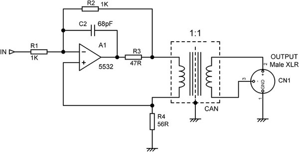
It is always necessary to use positive feedback with caution. Typically it works, as here, in conjunction with good old-fashioned negative feedback, but if the positive exceeds the negative (this is one time you do not want to accentuate the positive) then the circuit will typically latch up solid, with the output jammed up against one of the supply rails. R4 = 56 Ω in Figure 14.20 worked reliably in all my tests, but increasing it to 68 Ω caused immediate problems, which is precisely what you would expect. No input DC-blocking capacitor is shown in Figure 14.20, but it can be added ahead of R1 without increasing the potential latch-up problems. The small Sowter 3292 transformer was used.
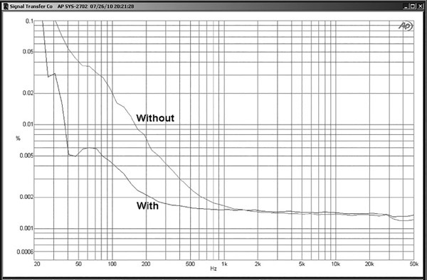
This circuit is only a basic demonstration of the principle of cancelling primary resistance, but as Figure 14.21 shows it is still highly effective. The distortion at 100 Hz is reduced by a factor of five, and at 200 Hz by a factor of four. Since this is achieved by adding one resistor, I think this counts as a definite triumph of brains over brawn, and indeed confirmation of the old adage that size is less important than technique.
The method is sometimes called “mixed feedback”, as it can be looked at as a mixture of voltage and current feedback. The principle can also be applied when a balanced drive to the output transformer is used. Since the primary resistance is cancelled, there is a second advantage as the output impedance of the stage is reduced. The secondary winding resistance is however still in circuit, and so the output impedance is usually only halved.
If you want better performance than this—and it is possible to make transformer nonlinearity effectively invisible down to 15 Vrms at 10 Hz—there are several deeper issues to consider. The definitive reference is Bruce Hofer’s patent, which covers the transformer output of the Audio Precision measurement systems.[6] There is also more information in the Analog Devices Opamp Applications Handbook.[7]
References
1. Self, D. Small Signal Audio Design. 2nd edition. Focal Press, 2015, pp. 607–608. ISBN: 978-0-415-70974-3 (hbk) ISBN: 978-0-415-70973-6 (pbk) ISBN: 978-1-315-88537-7 (ebk).
2. Self, D. Small Signal Audio Design. 2nd edition. Focal Press, 2015, pp. 527–535.
3. Sowter, G. A. V. “Soft Magnetic Materials for Audio Transformers: History, Production, and Applications” Journal of Audio Engineering Society, Volume 35, #10, Oct 1987, P. 769.
4. Otto von Bismarck Speech, 1862. (Actually, he said blood and iron).
5. Finnern, T. Interfacing Electronics and Transformers. Hamburg: AES preprint #2194 77th AES Convention, Mar 1985.
6. Hofer, B. Low-Distortion Transformer-Coupled Circuit. US Patent 4,614,914, 1986.
7. Jung, W., ed. Opamp Applications Handbook. Newnes, 2004. Chapter 6, pp. 484–491. ISBN 13: 978-0-7506-7844-5.