
Chapter 10
Moving-Magnet Inputs
Discrete Circuitry
Discrete MM Input Stages
Moving-magnet (MM) input stages constructed from discrete transistors have certain advantages. They are not limited to opamp supply rail voltages. They do not produce complex distortion products or crossover distortion like some opamps. The circuit operation is completely under the designer’s control, and every parameter, such as each transistor’s collector current, can be chosen by the designer. This chapter examines how to use that freedom of design and at the same time gives an historical overview of MM phono stages.
Discrete moving-magnet (MM) input amplifiers were almost universal until the early 1970s. For a long time opamps had, quite deservedly, a poor reputation for noise when used in this application.
When the first bipolar transistor MM inputs were designed, active components were still expensive, and adding another transistor to a circuit was not something to be done lightly. The circuitry from that era therefore looks to us very much cut-to-the-bone, but before disrespecting it we need to remember that it was designed under very different economic constraints.
A major problem with early discrete MM amplifiers was a simple lack of open-loop gain to give an accurate RIAA response network in the low-frequency region, even if the RIAA network was accurate, which it rarely was. Another problem was that an RIAA feedback network, particularly one designed for low closed-loop gain, and/or a relatively low RIAA network impedance to reduce noise, presents a heavy load at high frequencies because the impedance of the capacitors becomes low. Heavy loading at HF was commonly a major cause of increased distortion and headroom-limitation in discrete RIAA stages that had either common-collector or emitter-follower output topologies with asymmetrical clipping behaviour; an NPN emitter-follower is much better at sourcing current than sinking it. The 20 kHz output capability, and thus the overload margin, was often brought down by 6 dB or even more. Replacing the emitter resistor of an emitter-follower with a current source gives a much better HF output current capability, and this can be further doubled for the same quiescent dissipation by using a simple push-pull Class-A output structure.
One-Transistor MM Input Stages
I will say at once that the one-transistor MM input stage is purely an historical curiosity. Its performance cannot be expected to be anything other than dreadful by today’s standards. Nevertheless, the idea is worth looking at. Figure 10.1b shows a one-transistor MM input stage designed by Jack Dinsdale (of whom more later) in 1961.[1] At that time transistors were very expensive, and using two in a single stage would have been thought highly extravagant.
If you have but one transistor to play with, there are only three possible configurations; common-collector, (i.e. emitter-follower) common-base, and common-emitter. The first gives no voltage gain, and the second has a low input impedance that looks unpromising. That leaves the common-emitter configuration, as in both halves of Figure 10.1. Since it inherently inverts, the only possibility is shunt feedback, which as we saw in Chapters 7 and 9 is inherently much noisier than its series-feedback equivalent. The standard approach at the time, derived from valve designs, was that in Figure 10.1a, which had an input resistor R1 of 47 kΩ to give the correct cartridge loading, with the RIAA equalisation performed by the negative feedback network C1, R2, C2 in conjunction with the impedance of the collector load R3.

This arrangement is bound to give a poor noise performance. Dinsdale’s solution, in Figure 10.1b, was to make the input impedance low and implement the LF part of the RIAA equalisation by the interaction of the cartridge inductance with it, giving a 6 dB/octave slope. As frequency falls, the impedance of the inductance falls and the current into the input increases. He described this method as more “efficient”, which presumably means a greater transfer of energy through R1 and hence a better signal/noise ratio. Components R5 and C3 set the DC conditions, with base bias provided through R4.
The idea of loading the MM cartridge inductance with a low input resistance to achieve the LF boost section of the RIAA equalisation has come back to haunt us many times since then. The terrible snag is that since the LF equalisation is set by the cartridge inductance, changing the cartridge type almost certainly means you have to change the loading resistor too. You can of course add a control marked “cartridge inductance”, but this assumes you actually know the cartridge inductance, and know it precisely. Inaccuracy in the inductance setting will give errors in the RIAA response. You will have to rely on the manufacturer’s technical specification for the value of the inductance—which is usually given in suspiciously round figures—unless you plan to measure it yourself. That means acquiring an expensive precision component bridge and taking great care that you do not apply an excessive test signal. The two channels are unlikely to be identical, so you will need custom values for each channel. This is not a route many people are going to want to take, and for this reason, throughout this book you will find that the idea of using the cartridge inductance as a critical part of the RIAA equalisation receives very little sympathy.
Two-Transistor MM Input Stages
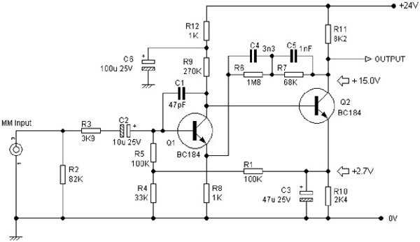
Figure 10.2 shows a typical two-transistor MM input amplifier from the late ’60s. The configuration is generally considered to have been introduced by Jack Dinsdale in 1965, in a classic preamplifier design[2] that was one of the first to deal effectively with the new RIAA equalisation requirements for microgroove records. It is a two-stage series-feedback amplifier composed of two common-emitter stages. R3 and C1 make up an RF filter; note R3 is 3k9; this is considerably greater than the DC resistance of most MM cartridges and looks like it would introduce unnecessary Johnson noise and unhelpfully convert the current noise of Q1 into voltage noise. The RIAA network is R6, R7, C4, C5, and it has a high impedance to reduce loading on the stage output. Since R6 has the high value of 1M8, the RIAA network cannot be used for the DC feedback that is required to set the quiescent conditions. There is a separate DC feedback network comprising R1, R4, R5, R10, and C3 which establishes the appropriate voltage across R10. C3 keeps signal frequencies out of this path. The RIAA network is in Configuration-A (see Chapter 7). No attempt is made to implement the IEC Amendment, as it was not introduced until 1976.

Because of its simplicity, this stage inevitably contains compromises. The second collector resistor, R11, needs to be high in value to maximise open-loop gain but low to adequately drive the RIAA network and any external loading.
An MM preamp has to deliver a maximum low-frequency boost of nearly 20 dB, on top of the gain required to get the desired output level at 1 kHz. If the cartridge output is taken as 5 mV rms at 1 kHz and the amplifier output is 150 mV rms (which is about as low as you could hope to get away with then if you were sending this signal to the outside world), then a total closed-loop gain of 20 + 34 = 54 dB is required at low frequencies. The open-loop gain obviously needs to be considerably higher than this, for a decent feedback factor is required not only to reduce distortion but also to ensure that the RIAA equalisation is accurately rendered by the feedback network. By 1970 it had become clear that the two-transistor configuration was really not up to the job, and more sophisticated circuits using three transistors or more were developed, aided by falling semiconductor cost. While the two-transistor MM preamplifier must now be regarded as of purely historical interest, it is highly instructive to see just what can be done with it by modification.
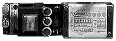
The circuit shown in Figure 10.2 was deliberately chosen as representative of contemporary practice in its era, and it has not been modified or optimised in any way. It is closely based on a small RIAA preamplifier PCB called the “Lenco VV7”, which was intended for upgrading systems to use MM cartridges where the amplifier had only a ceramic pickup input; see Figure 10.3. It was a Swiss product distributed in Britain by Goldring in the early 1970s. It had an integral mains PSU (see the tiny transformer on the left) with half-wave rectification and RC smoothing. What the proximity of that transformer did to the hum levels I do not know, but it looks awfully close to the preamp, which is in the screening can to the right. You will note that the single-rail supply is by modern standards low, at +15V; opamp-based preamplifiers today normally run from ±15V or ±17V, giving them a 6 dB headroom advantage at once. The gain is +39 dB at 1 kHz.
I built up Figure 10.2 with BC184 transistors, using an external DC supply. I found that the first-stage (Q1) collector current was 42 uA, and the second-stage (Q2) collector current was 0.63 mA. On measuring it I was not exactly surprised that the performance was mediocre. There was a high level of hum at the output: −66 dBu at 50 Hz. Carefully screening the whole circuit only reduced this to −68 dBu, so electrostatic pickup was clearly not the only or even the major problem.
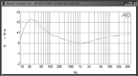
The RIAA equalisation accuracy, shown in Figure 10.4, is not good, which is only to be expected when you look at the standard component values in the RIAA network. Accurate RIAA networks cannot have more than one preferred value. The errors reach +2.3 dB at 20 Hz and +0.7 dB at 20 kHz; the IEC amendment is not implemented; it would have given an extra attenuation of −3.0 dB at 20 Hz and −1.0 dB at 40 Hz. The roll-off below 20 Hz is caused by C3. Increasing it from 47uF to 100uF much reduces the roll-off and slightly improves RIAA accuracy between 20 and 200 Hz.

The preamplifier was being powered from a perfectly respectable bench PSU, but it still seemed possible that hum was getting in from the supply rail, as there is absolutely no filtering in the supply to Q1 collector. Inserting a 1 kΩ–22 uF RC filter in the supply to R9 dropped the noise output from −68 to −73.4 dBu. (This figure is the average of six readings, to reduce the tendency of a noise reading to jump about when there is significant low-frequency content. Measurement bandwidth is always 22 Hz–22 kHz unless otherwise stated.) A bandpass sweep of the noise output showed that there was now very little extra 50 Hz or 100 Hz content. The RC filter gives an attenuation of −16.9 dB at 50 Hz and −22.8 dB at 100 Hz. Increasing the filter capacitance to 100uF however did give a slight improvement, so this was adopted; the attenuation at 50 Hz is now −29.9 dB.
Maximum output with a +15V supply rail was 3.4 Vrms at 1 kHz, (1% THD) so the maximum input was 38 mV rms, giving an overload margin of only 17.6 dB. It is noticeable that clipping is not symmetrical, occurring first on the positive peaks. When this clipping does occur, there is a shift in the DC conditions of the circuit due to the way the biasing works through the filtering action of C3.
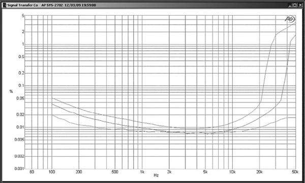
The THD at 1 Vrms out (1 kHz) was 0.010%, which by modern standards is a lot for such a low level. Figure 10.5 shows the distortion performance with a +15V rail, at 1, 2, and 3 Vrms out. The input signal was inverse RIAA equalised so that the output level remains constant with frequency. It was necessary to use the 100 Hz filter on the AP to get consistent results, despite having got rid of the 50 Hz problem with the RC filter, as there is still a large LF noise component due to the RIAA LF boost.
You can see that for 1 Vrms, the mid-band distortion is around 0.01%, but there is a steady rise below 1 kHz. This is caused by the falling negative feedback factor as the RIAA curve demands more gain at lower frequencies. The other area of concern is at high frequencies; at 1 Vrms nothing too bad happens in the audio band, though THD has reached 0.02% at 20 kHz.
At the higher output level of 2 Vrms, the mid-band THD is tripled. The output stage starts to clip around 15 kHz, as Q2 can no longer drive the RIAA network, which has a falling impedance at high frequencies. Things are pretty gross at 3 Vrms out, with THD around 0.1% mid-band and HF clipping starting at 4 kHz.
Clearly this historical RIAA preamp could use a bit of improvement, starting with linearity and headroom. Let’s see what can be done with it; the process will reveal a lot about how discrete circuitry works.
Two Transistors: Increasing Supply Voltage to +24 V
A pretty sure bet for improving both the linearity and headroom of a discrete amplifier is simply to increase the supply voltage. We will start by turning it up to +24 V, a voltage that can conveniently be obtained from a 7824 IC regulator. Figure 10.6 shows the results; distortion is somewhat reduced overall, and the HF overload problem has been pushed to slightly higher frequencies, but the effect is not as dramatic as we might have hoped. The maximum output has only increased to 3.8 Vrms at 1 kHz (1% THD), which is not much of a return for increasing the supply voltage by 60%.

Casting a suspicious eye over the circuit, it’s clear that it is still clipping asymmetrically. There is +18.4V on Q2 collector, whereas for a symmetrical output swing we would expect something more like +12 V. Improving the bias conditions by changing R10 from 3k9 to 2k4 reduces Q2 collector volts to +15.0V and gives much more output voltage swing capability, as well as increasing the standing current in Q2, which improves load-driving capability. The maximum output is now 6.0 Vrms at 1 kHz, an improvement of +4 dB. The input overload margin is raised to 23 dB. While this rebiasing does not give exact symmetry of clipping, it does seem to be close to optimal biasing for linearity. A good indication of this is that the distortion residual at 1 kHz is third harmonic, which suggests that some cancellation of second-harmonic distortion is going on.
The distortion performance is transformed; 3 Vrms out (1 kHz) gave 0.06% in Figure 10.6. After rebiasing it has fallen to 0.014%, as in Figure 10.7. The HF overload effect has also been pushed out to above 20 kHz, even for the 3 Vrms case. Not bad for modifications that essentially cost nothing.
The distortion improvement at lower output voltages in the mid-band is barely visible even with 100 Hz AP filtering because of the high noise output from a circuit with +39 dB of gain at 1 kHz.
The modified circuit, with the added RC filter for the first stage, supply increased to +24 V, and biasing adjusted by changing R10, is shown in Figure 10.8. The Ic of Q1 is now 75 uA, and the Ic of Q2 is 1.1 mA.
Two Transistors: Increasing Supply Voltage to +30V
Since increasing the supply to +24 V gave considerable benefits (after rebiasing), we will increase it further to +30 V. This increases the maximum output to 6.8 Vrms at 1 kHz (1% THD), which is 6 dB up on the original circuit. The input overload margin is raised to 24 dB. R10 has been changed again to 2k2 to optimise the biasing. The results are seen in Figure 10.9. The THD for the 1 Vrms case is now completely submerged in low-frequency noise, so I used the 400 Hz AP filter, which shows the THD at 1 Vrms (1 kHz) is about 0.0055%. This number however still contains a significant amount of noise.
HF overload behaviour has improved again, but HF distortion is somewhat worse at all three output levels. The LF distortion is notably improved, being more than halved.
As a side issue, we might consider how to generate the supply rail required. The 7824 IC regulator will accept a maximum input of 40 V, so it is feasible to use that with the ADJ pin elevated by some means, as described in Chapter 16. For output voltages above +30V this does not leave enough regulator headroom, and we might need to use the TL783 high-voltage regulator. This is a favourite device for generating +48 V supplies for microphone phantom power and can definitely be relied on up to this voltage.
Two Transistors: Gain Distribution
At this point I began wondering what else could be done to reduce the distortion. There are practical limits to raising the supply voltage; power dissipation increases, and there is a danger that the circuit could generate turn-on or turn-off transients that would damage stages downstream.
At this point it’s worth considering what the sources of nonlinearity are. The two transistors, obviously, but the RIAA capacitors could also be contributing, as I used ordinary polyester types, and if you’ve read the chapter on components, you will know that these are not wholly linear, and in this application there is a significant signal voltage across them. However, the distortion generated by polyester caps is typically of the order of 0.001% at 10 Vrms, and the signal levels we are using here are much lower than that, so the capacitor contribution is almost certainly negligible. At the time of writing I haven’t got round to proving the point by substituting polypropylene capacitors, which are linear.
The configuration is made up of two cascaded voltage amplifiers, and it seemed to be a good idea to find out how the open-loop gain is distributed between them. The high value of the Q1 collector load suggests that it is intended to give a high-voltage gain.
Measurement showed that the signal on Q1 collector was −49 dB with reference to that on the output at Q2 collector, at 1 kHz. This was confirmed by SPICE simulation, which gave −45 dB on Q1 collector between 100 Hz and 10 kHz. Note however that the emitter of Q2 is connected to AC ground via C3, which suggests that the second stage has a low input impedance and perhaps the first stage is working as a transconductance stage, feeding a current into the base of Q1 rather than a voltage, if you see what I mean. SPICE gives the error voltage, i.e. that between the base and emitter of Q1, as 38 dB below the output voltage, so the voltage on Q1 collector is less than that going into the first stage, and this indicates that Q1 is indeed feeding a current to Q2. This is an important finding as it means that the open-loop gain, and hence the feedback factor, cannot be increased by bootstrapping the collector load of Q1, which was the idea I had at the back of my mind all along.
The low impedance at Q2 base will be further reduced by Miller feedback through the Cbc of Q2, though how significant that is is uncertain at present. Since Cbc is a function of collector voltage, this is another potential source of nonlinearity.
Two Transistors: Dual Supply Rails
The question arises as to how easy it would be to convert this stage to run off dual supply rails, i.e. ±V and 0V. The answer appears to be—not easy at all, because the input transistor Q1 that performs the input-NFB subtraction is sitting very near the bottom rail.
Two Transistors: The Historical Dinsdale MM Circuit
The first two-transistor MM stage is generally accepted to have been put forward by J. Dinsdale, in an article “Transistor High-Quality Audio Amplifier” in Wireless World for January 1965. This article may be 45 years old, but it is still worth reading if you can got hold of it, not least because it discusses how to make an MM preamplifier using just one transistor; see the start of this chapter to find how to do it and why not to do it.
You will note at once from Figure 10.10 that the circuit is upside-down to modern eyes, with a negative supply rail at the top. I find the electrolytics particularly unsettling. This was common in circuits of the era and stemmed from the fact that most germanium transistors were PNP, so if you drew the emitter at the bottom (which is where people were used to drawing valve cathodes) then inevitably you end up with a negative supply rail at the top. When silicon transistors came in, they were more commonly NPN, so a sigh of relief went up all round as we reverted to the more logical approach of having the most positive rail at the top.
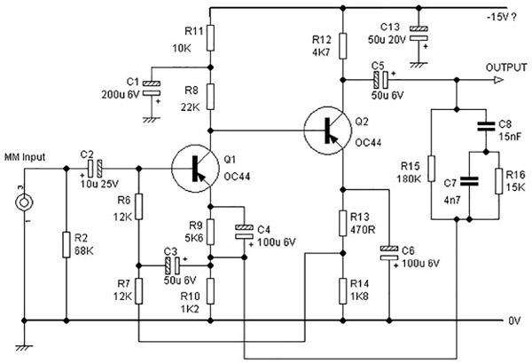
I have not so far tried building this circuit, due to the difficulty of obtaining the transistors. The OC44 was a PNP germanium transistor made by Mullard. Remarkably, it is still in much demand—in fact it has achieved iconic status—as it is held to give a unique sound in vintage-style fuzz boxes.[3], [4], [5]
Comparing this circuit with Figure 10.2 you can see that there are the characteristic two separate feedback loops, with DC feedback through R13, R14, and R7 and AC feedback to Q1 emitter via the RIAA network R15, C8, R16, C7. The DC path through this network is blocked by C3. The RIAA network is in Configuration-B (see Chapter 7). There is no IEC Amendment.
C3 bootstraps R6 to raise the input impedance high enough to give 47 kΩ in conjunction with loading resistor R2; disconcertingly Dinsdale refers to this as “feedback” in his article, which it is not.
The supply rail voltage is not precisely known, as in the complete preamplifier circuit the MM stage is fed through a network of RC filters that leave the final voltage in some doubt. It clearly is not greater than −20V, judging by the rating of C13, and it seems pretty safe to assume it was around −15V. However the OC44 had a collector breakdown voltage of only 15V, so the rail might have been lower—perhaps −12V.
This circuit uses more parts than the two-transistor circuit of Figure 10.2, largely as a result of the different DC bias arrangements. Apart from the transistors, it has twelve resistors and five electrolytic capacitors. Figure 10.2 has (ignoring EMC filtering) ten resistors and two electrolytic capacitors and is the more economical solution.
Three-Transistor MM Input Stages
Adding an extra transistor improves the possible performance remarkably. An early three-transistor configuration was introduced by Arthur Bailey in 1966,[6] though his version had a rather awkward level-shift between the first and second transistors. Figure 10.11 shows a much improved version from the early ’70s, designed by H. P. Walker[7] and later enhanced by my own good self.[8] It consists of two voltage amplifier stages as before, but an emitter-follower Q3 is added to buffer the collector of the second transistor from the load of the RIAA network and any external load. This means that the second transistor collector can be operated at a much higher impedance, generating more open-loop gain.

The original Walker design had a simple 22 kΩ resistor as a collector load for Q2; when I was using this configuration[8] I split this into two 12 kΩ resistors, bootstrapping their central point from the emitter of Q3, as shown in Figure 10.11; this further increased the open-loop gain and reduced the distortion by a factor of three. With the wisdom of hindsight I strongly suspect that C6 should be increased in size; its LF roll-off in conjunction with R10 (R12 is not involved) is at 6 Hz, but that misses the point. For bootstrapping to work properly the signal voltage at the top capacitor terminal must be identical to that at the bottom, which needs a very low roll-off frequency. If C6 is increased to at least 47uF, the LF distortion should be reduced. Dominant-pole compensation is applied to Q2 by C1. Once again, the RIAA network has a high impedance, and a separate path for DC feedback must be provided by R1; there is in fact no DC feedback at all through the RIAA network because it is connected to the outside of C9. R3 and C8 are the input RF filter. The supply to the first stage is heavily filtered by R8 and C5.
The RIAA network is in Configuration-A. There is no IEC Amendment, as it was not introduced until 1976.
The added emitter-follower Q3, running at a much higher collector current than Q2 (5 mA versus 500 uA), much increases the output voltage swing into a load and so improves the input overload margin. However, a simple emitter-follower output stage has an asymmetrical output current capability, and so this is less effective at high frequencies where the impedance of the RIAA network is falling. Low-gain versions of this circuit may have the overload margin compromised by several dB at 20 kHz. This can be overcome by making the output stage more sophisticated—replacing the emitter resistor R4 with a current source greatly improves matters, and using a push-pull Class-A output doubles the output current capability again.
While this stage is a great improvement on the two-transistor configuration, it also is not well-adapted to dual supply rails, for the same reason; Q1 is still referenced to the bottom rail.
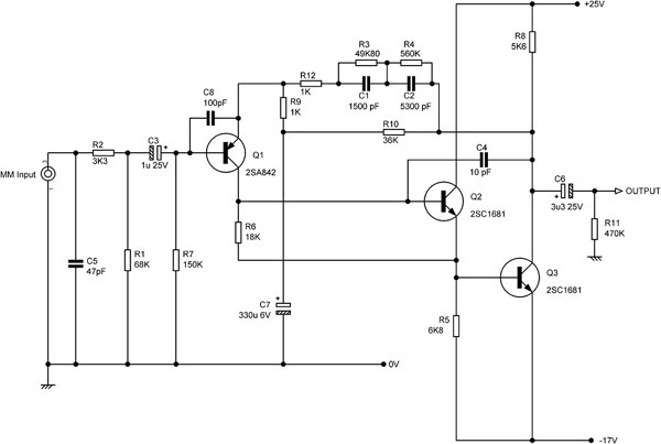
Figure 10.12 demonstrates another way to use three transistors in an RIAA amplifier; this configuration consists of a voltage amplifier stage, an emitter-follower, and then another voltage amplifier stage. The RIAA network is in Configuration-A. The first transistor is now a PNP type, its collector bootstrapped for increased gain by connecting the lower end of collector load R6 to the emitter-follower Q2. R2 and C8 make up an RF filter, and once more there is a high value of series resistance. Q2 drives the output transistor Q3, which is now a common-emitter voltage amplifier with collector load R8. Note the asymmetrical supply voltages; the positive rail is 8 V greater than the negative rail, and this is almost certainly intended to increase the positive-swing capabilities of the Q3 stage. Once again note the high impedances in the RIAA network to reduce the loading on the output and the consequent need for a separate DC feedback path via R10, the AC content being filtered out by C7. Versions of this configuration were used by Pioneer and Sonab.
Four-Transistor MM Input Stages
All of the amplifiers described so far have conventional output stages and so have trouble driving their RIAA network at high frequencies. Going from three transistors to four gives much greater freedom of design and allows us to use a markedly more capable output stage. Since Q1 is no longer connected to the bottom rail, the use of dual supplies is possible. The design in Figure 10.13 is closely based on the MM input stage of my “High-Performance Preamplifier” published in Wireless World in 1979.[9] By my own internal labelling system this was the MRP4. A slightly modified version (the MRP6) was used a year later in a preamplifier design for a consultancy client.
The MRP4 was the first “conventional” preamplifier design, insofar as my designs are ever conventional, that I published. It was my own reaction to the considerable complexity of the Advanced Preamplifier of 1976,[8] with its multiple discrete opamps. Back then the available IC opamps were looked at with entirely justified suspicion; they were relatively noisy and prone to crossover distortion in their output stages. Crossover might be inescapable in power amplifiers of the day, but it was definitely not acceptable in a preamplifier. Thus discrete Class-A circuitry was used throughout the preamplifier. (The 5534 opamp was just becoming available at the time but was horribly expensive.)
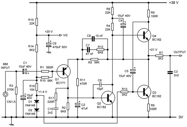
This design was intended to showcase a very large overload margin, and so its gain at 1 kHz was only 10 times (+20 dB), and the output was only 50 mV rms nominal. Obviously, further downstream amplification (of variable gain) was required to get the signal up to a level that could be applied to a power amplifier. The configuration is much the same as many power amplifiers of the day, and if the singleton input transistor was replaced by a differential pair, it would look very much like the “model amplifiers” used so extensively in my book Audio Power Amplifier Design.[10]
I used a single-transistor input because I was worried about the noise contribution from the second transistor in a differential pair. That this might create a relatively large amount of second-harmonic distortion was considered of less importance, given the 50 mV rms nominal output of the stage. The RIAA network is an example of Configuration-C, which is preferred because of its lower capacitor values for the same gain and impedance, as described in Chapter 7. It has capacitor values similar to those used in the +30 dB gain opamp MM inputs in that chapter, but R0 (which in Figure 10.13 is actually labelled R11) is larger, so the gain is 10 dB less. The stage could accept an input of 1.1 V rms at 1 kHz, an overload margin of no less than 47 dB, and 3.8 Vrms at 10 kHz. The low gain made an HF correction pole (R7, C3) essential. No attempt was made to implement the IEC Amendment.
The whole preamplifier ran off a single +38 V rail that was not regulated; instead it had a post-reservoir RC filter that reduced the supply ripple to about 50 mV rms. This low-cost approach was combined with heavy RC decoupling of the bias network for each stage, and this was very effective at getting low hum figures.
The biasing network R14, R15, R16, D1, D2 provides three voltages. The +20 V “V/2” bias rail was used throughout the rest of the preamplifier; it is heavily filtered by the large value of C9. The bias voltage at the top of R16 was lower to allow for the voltage drop of Q1 collector current through R5. This voltage-shift is an inherent problem with singleton inputs. D1, D2 provide the bias for the push-pull output stage and were shared between the left and right inputs without any crosstalk problems.
The input impedance is defined by resistors R10 and R1 in series, in parallel with DC drain R3; this comes to 46.8 kΩ. You will note that all the resistors in the stage (including those in the RIAA network) are E12, because E24 value resistors were specialised and expensive parts back in those days and rarely if ever used in audio work. With the clarity of hindsight, I should have made C1 larger, say 47 or 100 uF, to minimise the effect of LF current noise.
The collector current of Q1 is set by the Vbe of Q2 maintained across R2 and is here 53 uA. The signal is passed as a current from Q1 to the VAS Q2, on whose collector the full output swing is developed. Q2 collector load was a bootstrapped resistor rather than a current source, as this still gave an economic advantage at the time. This is then buffered by the push-pull emitter-follower Q4 with its driven current source Q3; R9 senses the current through Q4, and when it increases the voltage on Q3, base is reduced via C5. Since this is effectively a negative-feedback loop with a gain of unity and 100% feedback, the current variations are halved for a given load, and so the peak output current is doubled.
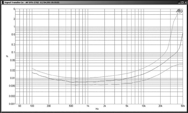
Stability is an issue here because the amplifier is working with a closed-loop gain close to unity at HF. The Miller dominant-pole capacitor, C6, is made as small as possible to maximise the slew rate, and stability is assisted by the lead-lag network R17, C10 across Q1 collector resistor. This stage was followed by a 3rd-order subsonic filter using a current-source emitter-follower, and the only THD figure I have to hand is for both stages together. THD was below 0.004 % at 6 Vrms out, from 1 kHz to 10 kHz, the input signal being inverse RIAA equalised to give constant output with frequency.
This design could be relatively easily converted to run off dual supply rails, as the first transistor is not referenced to the bottom rail. However, the voltage drop through R5 is a problem, for if Q1 is biased from 0V, the output standing voltage will be several volts positive.
Five-Transistor MM Input Stages
A good number of phono amplifiers that were considered advanced in their day used five transistors. One example that comes to mind was in the Lecson AC-1 preamp (1975), though perhaps it doesn’t really count, as one of the devices is used for electronic switching. A famous five-transistor example is from the Radford ZD22 (1973) shown in Figure 10.14; this was considered one of the most advanced preamplifiers of its day. Interestingly, the designer (according to John Widgery, that was Jens Landvard, a Scandinavian freelance designer who also designed the Radford ZD100 and other products) chose exactly the same Ic for the input transistor that I did.
You are probably looking at the output stage and muttering about Class-B and how crossover distortion is absolutely impermissible in a preamplifier. In fact, the output stage really is in AB mode, unlike power amplifiers that claim to be. Since there are only two transistors and not the driver-output combination of a power amplifier, the transition of conduction from one transistor is much smoother and there is no crossover distortion as such, though the stage is less linear than a Class-A version; see Small Signal Audio Design[11] for more on this. The output stage has excellent drive capabilities and a low-impedance RIAA network in the capacitor-efficient Configuration-C is used, with precision components (for their day) used in the critical positions.

The single +50V supply rail permits a maximum output of about 17 Vrms. The gain is +33.9 dB (1kHz), which gives an excellent maximum input of 357 mV rms (1kHz) and a very healthy overload margin of +36 dB. At this relatively low gain an HF correction pole R17, C14 is essential to keep the RIAA accurate at the HF end. In simulation the RIAA accuracy is very flat in the middle but −0.1 dB at 200 Hz and 10 kHz. The LF end rolls off due to the subsonic filter implemented by C8, C9, R9, C10, R10; this does not give any known filter characteristic but shows a −0.4 dB shelf between 50 and 100 Hz, followed by a roll-off at roughly −9 dB/octave that is −10 dB at 20 Hz and −18 dB at 10 Hz. The HF end rolls off because (from my simulations) the HF correction pole has the wrong value; changing C14 to 2n2 pushes the −0.1 dB point out to 20 kHz. Aside from that, it’s a fine piece of design work.
Six-Transistor MM Input Stages
If we permit ourselves one more transistor, bringing the total to six, the MM stage of Figure 10.13 can be significantly improved in its distortion performance. The MM preamplifier in Figure 10.15 was used in an experimental preamplifier which according to my own numbering system was the MRP2; it was not published. It was designed with less regard to economy than the MRP4 and was therefore somewhat more sophisticated despite it coming earlier in the series.
In this preamplifier, as in the MRP1, the RIAA equalisation was performed in two stages, with the HF part of the RIAA implemented by R8, R9, C4, C5 in the first stage to give good headroom at high frequencies. The gain is +26 dB (1kHz) and the maximum output of 12.4 V rms, giving a huge maximum input of 620 mV rms and an overload margin of 42 dB. The LF boost part of the RIAA was performed by the normalisation amplifier downstream, which raised all the inputs to the same nominal level. The LF boost components were switched out of the feedback loop when a line input was in use and a flat response required.

The configuration is again essentially that of the solid-state power amplifiers of the day, which tended to use a single input transistor to perform the feedback subtraction, the great advantages of the differential pair for low distortion as well as DC precision not being much appreciated at this point. A single input transistor was used here with the aim of minimising noise, working on the assumption that two transistors must be noisier than one, though in this case not 3 dB worse, as the NFB network has a much lower impedance than the cartridge. The input transistor has its collector current defined at about 88 uA by the 0.6V established across R6; this apparently low value gives a better noise performance than higher currents, with the highly inductive source resistance of an MM cartridge. Q1 passes its output current to the voltage amplifier stage, or VAS, and its transconductance combined with the value of the dominant-pole Miller capacitor C9 sets the open-loop gain at high frequencies. As in Figure 10.14, C1 would have been better made 47 or 100 uF.
The main sources of distortion in the VAS are Early effect and the nonlinear variation of Cbc with Vce. A cascode VAS reduces both effectively; the collector voltage of Q4 is kept constant by Q3, and so there is no Early effect. Likewise, since there is no signal on the collector of Q4 there can be no local negative feedback through its nonlinear Cbc, and the compensation feedback all goes through C9. Similar and perhaps slightly better results would be obtained by omitting the cascode transistor Q3 and putting an emitter-follower inside the C9 Miller loop. The first version of this circuit had a simple current-source emitter-follower output, running at the same quiescent current of 9 mA; it showed premature negative clipping at high frequencies due to the heavy loading of the HF RIAA capacitor in the feedback network, and also loading by the HF correction pole R15-C8; this problem was almost totally eliminated by converting it to the same push-pull Class-A White output structure as used in Figure 10.13.
Everything is biased from a single divider D1-D2-R2-R3-R4, which is heavily filtered by C2 to remove supply rail noise. The voltage across R4 is 1.2 V and biases both the cascode transistor Q3 and the push-pull output current-source Q6. So far as I’m concerned, this configuration may have six transistors, but it does not count as a “discrete opamp” because there is no differential input. As for the four-transistor version, there should be no difficulty in converting it to dual-rail operation, because the biasing system is not referenced to the bottom rail. Because a single input transistor does not have the DC precision of a differential pair, and there is a voltage drop across feedback resistor R8, there will be a significant offset voltage at the output, which will need to be DC blocked by a series capacitor.
The input impedance is set by the parallel combination of R1 and R5, which is 46.4 kΩ. This is a little low compared with the nominal value of 47 kΩ, representing an error of 1.3%, but it is the best you can do with two E12 resistor values; bear in mind that R5 should not be too big (say 100 kΩ or less) as it carries the base current for Q1 and there will be a voltage dropped across it. At the time of the design E24 resistors were relatively rare and expensive, and no consideration was given to using them to get parameters like the input impedance more accurate. Using E24 resistors R1 = 300 kΩ and R5 = 56 kΩ gives an input impedance of 47.2 kΩ, an error of only 0.4% in the nominal value; note this error does not include the effects of resistor tolerances.
Even greater accuracy could be achieved by using three E24 resistors in parallel. For example R1 = 560 kΩ in parallel with 620 kΩ and R5 = 56 kΩ reduces the error in nominal value to 0.10% high, which is likely to be much less than the resistor tolerances. There are many combinations of three resistors that give a combined value very close to 47 kΩ, and adding the extra constraint that they should be as nearly equal as possible allows significant improvements in accuracy when tolerances are taken into account, as random errors partially cancel; this is explained in detail in Chapter 2. The three resistors 560 kΩ, 620 kΩ, and 56 kΩ show this effect to some extent; if 1% resistors are used the effective tolerance of the combination is slightly improved to 0.85%. A better choice would be R1= 160 kΩ in parallel with 200 kΩ and R5 = 100 kΩ, which has a nominal value only 0.12% high and an effective tolerance of 0.60%, which is significantly better.
More Complex Discrete-Transistor MM Input Stages
The record for the highest supply voltage to an RIAA stage was set in 1974 by the Technics SU9600, which used seven transistors and employed ±24 V rails and a third rail at a staggering +136 V. This gives a whole new meaning to the phrase “third-rail electrification”. To the best of my knowledge the record still stands. The general configuration is shown in Figure 10.16; seven transistors are used, in three cascaded differential voltage amplifiers, followed by an emitter-follower output buffer. The final voltage amplifier and the output stage work on asymmetrical supplies, running between +136 V and −24 V. The output sits at +56 V to allow a symmetrical output swing, which accounts for the DC-blocking capacitor C11. Note that several resistors around the output stage are high-wattage types. RV1 allowed gain adjustment, while RV2 and RV3 were for setting the DC conditions. My information is that the maximum input was 900 mV (frequency unstated, but presumably at 1 kHz), the THD was 0.08% (frequency and level unstated), the S/N ratio was 73 dB with reference to 2 mV, and the RIAA accuracy was ±0.3 dB.
The output device dissipation is of course enormous for a preamp stage, and the use of a constant-current source, or better still a push-pull Class-A output stage, would have allowed this to be much reduced; one can only speculate as to why those techniques were not used. There would probably have been some fearsome transients at the output on switch-on, and it is notable that an output muting relay was required, probably not so much for reducing audible noise as to give the later stages in the preamplifier a chance of survival.

In the original circuit small capacitors were freely sprinkled over the diagram, leading me to suspect that HF stability was a serious issue during development.
References
1. Tobey, R., and Dinsdale, J. “Transistor High-Fidelity Pre-Amplifier” Wireless World, Dec 1961, p. 621.
2. Dinsdale, J. “Transistor High-Quality Audio Amplifier” Wireless World, Jan 1965, p. 2.
3. www.californiavalveworks.com/Mullard.html Accessed June 2013.
4. http://swartamps.com/oc44_transistor_dallas_rangemaster.htm Accessed Nov 2016.
5. www.williamsaudio.co.uk/Williams-OC44-Ranger.html Accessed Nov 2016.
6. Bailey, A. R. “High Performance Transistor Amplifier” Wireless World, Dec 1966, p. 598.
7. Walker, H. P. “Low-Noise Audio Amplifiers” Electronics World, May 1972, p. 233.
8. Self, D. “An Advanced Preamplifier Design” Wireless World, Nov 1976.
9. Self, D. “High-performance Preamplifier” Wireless World, Feb 1979, p. 40.
10. Self, D. Audio Power Amplifier Design. 6th edition. Newnes, 2013, p. 190. ISBN 978-0-240-52613-3.
11. Self, D. Small Signal Audio Design. 2nd edition. Focal Press, 2015, pp. 562–568. ISBN: 978-0-415-70974-3 (hbk) ISBN: 978-0-415-70973-6 (pbk) ISBN: 978-1-315-88537-7 (ebk).