Chapter 10. Gating and Logic Circuits
Digital gate circuits. Logic actions for control of devices. Gate symbols. AND and OR and NOT gates. Symbols for gates. Boolean logic. Combinational circuits. Truth tables for simple gates. Boolean algebra. NAND and NOR gates. XOR gate. Analyzing gate circuits by truth tables. Combination lock example. Arithmetic circuits. Half-adder for two-bit addition. Full adder where a carry-in bit is used. Construction of full adder from gates. Series and parallel adders. Four-bit parallel adder example. Subtraction. Four-bit subtractor example. Borrow action. Multiplication and division. Use of registers. Code changing. Encoder and decoder action. Multiplexers and demultiplexers. Address number. Hexadecimal keypad example. Strobe pulse. Time-division multiplexing.
Gates
Digital circuits come in several varieties, but one very basic and important type is the
gate, which is used for controlling actions rather than just for counting. More than 100 years before digital electronics was established, an English mathematician called George Boole proved that all of the statements in human logic could be expressed by combinations of three rules which he called AND, OR, and NOT. This logic system is now known as
Boolean logic. We will see later how these gates can also be used for simple arithmetic actions.
Definition
Note
Definition
A gate in digital electronics means a circuit whose output is a 1 only for some specified combination of inputs. This type of circuit is sometimes referred to as a
combinational circuit.
Note
Do not confuse this with an
analog gate circuit, which switches an analog waveform on or off depending on the state of a gating input signal.
The importance of all this is that, if we can provide digital gate actions corresponding to these three rules of AND, OR, and NOT, we can construct a circuit that will give a 1 output for any set of logical rules. For example, if we want to have an electric motor switched on when a cover is down, a switch is up, and a timer has reached zero, or when an override switch is pressed, then this set of rules can be expressed in terms of AND, OR, and NOT, and a gate or set of gates can carry out the action.
Figure 10.1 shows the symbols that are used for the three main gate types, the AND, OR, and NOT gates, using two-input gates in the example. The action of these gates will be discussed in detail shortly, but for the moment note that the small circle shown in the NOT symbol is used to mean inversion, converting 1 to 0 or 0 to 1. We can combine the other basic symbols with the NOT circle symbol to give symbols for other gate actions. The early digital integrated circuits (ICs) would typically contain four gates of one type per chip, but modern electronic equipment is more likely to use custom-made chips, with all the gates and their connections formed in one process, using thousands or millions of gates on one chip.
 |
| Figure 10.1 Gate symbols for the basic actions of AND, OR, and NOT. These are the internationally used symbols and this drawing shows two variants on the OR symbol |
Once again, this makes it more useful to show block diagrams rather than gate circuit details. A gate circuit diagram will consist of a large number of gate symbols with joining lines so that the output of a gate will be connected to one or more other gate inputs. Provided that we know what each basic type of gate does, we can analyze the action of complete gate circuits. In this book we are concerned more with block diagrams than with gate circuits, but some knowledge of gate circuits is useful, and in any case, these are closer in spirit to block diagrams than to circuit diagrams.
Summary
Note
Definition
Summary
Logic circuits exist to carry out a set of logic actions such as are used for controls for washing machines, tape-recorder drives, computer disk drives, security systems, and a host of industrial control actions. Simple arithmetic actions can also be carried out using logic circuits. All logic actions, however complicated, can be analyzed into simple actions that are called AND, OR, and NOT, so that circuits, called gates, which carry out such actions, are the basis of logical circuits.
Note
Remember that ICs are classed as medium-scale integration (MSI), large-scale integration (LSI), very large-scale integration (VLSI), etc., by the number of equivalent gate circuits on a single chip.
Definition
The action of any gate can be expressed in a
truth table. This is just a table that shows all the possible inputs to the gate, and the output for each set of inputs. Remember that each input can be 0 or 1 only, so that each input contributes two possible outputs. The total number of outputs is equal to 2
n, where
n is the number of inputs.
For example, if there are four inputs to a gate, then the number of possibilities is 2
4=
16, and its truth table will consist of 16 lines. For a lot of truth tables, there is only one output that is different from the rest, and it is easier to remember which one this is than to try to remember the whole of a truth table.
Note
Note
Truth tables are the simplest way of showing what a small-scale gate or gate circuit does, but they are impossibly clumsy when we try to use them on complex gates with a large number of inputs. The more useful method for professional use is called
Boolean algebra but, like other mathematical methods, it is beyond the scope of this book. There are computer programs that will analyze the action of a gate circuit using Boolean algebra.
Figure 10.2 shows truth tables for the basic two-input AND, OR, and NOT gates. Of these, the NOT gate is a simple one, with just one input and one output. Its action is that of a logic inverter. If the input is 0, then the output is not0, which is 1. If the input is 1, then the output is not1, which is 0. The other two gate types permit more than one input, and the examples show two inputs, the most common number. The action of the AND gate is to give a 1 output only when both inputs are at 1, and a 0 output for any other combination. The action of the OR gate is to give a 0 output when each input is 0, but a 1 for any other combination of inputs. The same arguments apply to gates with more than two inputs.
Summary
Summary
A truth table is a simple but clumsy way of showing what the output of a gate or gate circuit will be for each and every possible combination of inputs. The alternative is to use Boolean algebra, a process that is greatly simplified by computer programs that carry out an analysis of gate circuits.
 |
| Figure 10.2 Truth tables for gates. The AND and OR gates are illustrated in two-input form |
NAND and NOR Gates
Two particularly useful gate types can be made by combining the action of an inverter with that of the AND and OR gates. The combination of NOT and AND gives the NAND gate, whose symbols and truth table (for two inputs) are shown in Figure 10.3. The action of this gate is that the output is 0 only when all of its inputs are at 1, which is the action of the AND gate followed by an inverter. The combined action of the OR gate and a following inverter gives the NOR gate, whose symbols and truth table are shown in Figure 10.4. The output of this gate will be at logic 0 when any one (or more) of its inputs is at logic 1.
 |
| Figure 10.3 The NAND gate, with symbol, truth table and equivalent gate circuit |
 |
| Figure 10.4 The NOR gate with symbol, truth table and equivalent gate circuit |
There is one further gate that is often used and which is called
exclusive-OR (XOR). This action (Figure 10.5) is closer to what we normally mean by the word ‘or’ (meaning one or the other but not both), and the output is 1 if either input is 1, but not when both inputs are zero or both are 1. The diagram also shows that the XOR gate is equivalent to the action of a circuit made using an OR, AND, and NAND gate combination.
Note
Summary
Note
If you would like to read further about gates and other logic circuits, with details of the more advanced methods such as Boolean algebra, take a look at the book
Digital Logic Gates and Flip-Flops, from PC Publishing.
Summary
A truth table is a simple way of expressing the action of a logic circuit, and the standard gates called OR, AND, and NOT can all be illustrated in this way. Gates in IC form often consist of the NAND and NOR type of gates, equivalent to an AND or OR, respectively, followed by NOT. These inverting gates are easier to produce and the action is often more useful than that of the simpler AND or OR type. The XOR gate is another useful type which gives an action closer to the normal meaning of OR, as ‘one or the other but not both’.
 |
| Figure 10.5 The XOR gate with truth table and equivalent gate circuit |
Analyzing Gate Systems
A circuit that has been made up by connecting several standard gates together, which has several inputs and an output, can be analyzed to find what its action is. This analysis can be done by drawing up truth tables, or by a method called Boolean algebra. The truth-table method is simpler, but more tedious than the Boolean algebra method, which is not dealt with in this book. The method of analysis by truth table can be summarized in a few rules.
1. Letter each input to the circuit (A, B, C) and also each point where the output of one gate is connected to the input of another gate, using different letters for each point. Label the final output as Q.
2. Draw up a blank truth table, using one column for each letter that has been allocated, and with 2
n rows, where
n is the number of signal inputs to the circuit.
3. Write in every possible combination of inputs. This is most easily done by starting with 0000 and continuing in the form of a binary count (0001, 0010, 0011, 0100, 0101) up to an input which consists entirely of 1s.
4. Knowing the truth tables for the standard gates, write in the logic states (0 or 1) for the outputs of the gates at the inputs in each line of the truth table.
5. The first set of outputs will now be the inputs for the next set of gates, so that their outputs can be written into the truth table.
6. Continue in this way until the truth table has been completed.
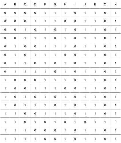
As an example, Figure 10.6 shows a logic diagram for an electronic combination lock. This is a simple design, with four main inputs, and therefore 16 combinations, ignoring the unlock input E. The lock is arranged so that only the correct combination of inputs will open the lock, and any other combination will cause an alarm to sound, so that it cannot be solved by trying each possible combination.
 |
| Figure 10.6 A gate circuit used as an example for analysis using truth tables |
The inputs, A, B, C, and D are from switches which are to be set in the pattern needed to open the lock. When these switches have been set, pressing the button E will cause the door to unlock (Q
=
1) if the combination is correct, or cause the alarm to sound (X
=
1) if the combination is incorrect. To analyze this digital circuit, label the inputs as shown in Figure 10.7.
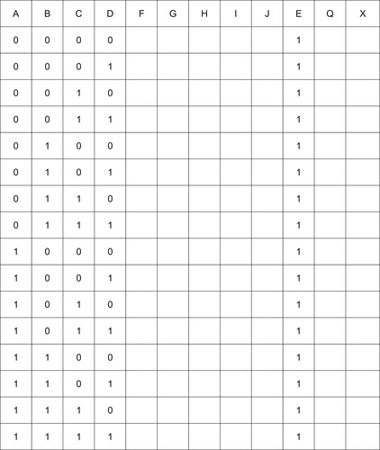 |
| Figure 10.7 The table with inputs filled in and intermediate values provided for |
The important inputs are A, B, C, and D, because E is used only after all the others have been set into the correct pattern. The intermediate points, where the output of one gate drives the input of another gate, can now be labeled F, G, H, I, and J as shown in Figure 10.7. Because there are four main inputs, 16 lines of truth table will be needed.
There will be one column for each letter which has been used, but the column for the E input can be placed next to the Q column because the E input is used only when the Q output is decided (after all the other inputs have been set). The logic voltage of E can be written as 1 in each row because the lock will act only when E is set to 1 (the activating button is pushed). All of the possible A, B, C, D inputs can now be written down, starting with 0000, and going through a binary count to 1111, a total of 16 rows in the truth table of Figure 10.7.
We can now analyze the circuit (Figure 10.8). Inputs A and B are inputs of a NAND gate. whose logic is that the output is 0 only when both inputs are 1. The F column, which is the output of this gate, therefore has a 0 entered for the last four rows of the table, when both A and B are at logic 1, and a 1 entered for all other rows The G column is just the inverse of the C column, so that its values can now be written in.
 |
| Figure 10.8 The table completed, using the truth tables for the gates to fill in the intermediate values |
The values in the H column are the outputs of another NAND gate whose inputs are G and D, so that the output is 0 only when G
=
1 and D
=
1, as shown. The values in columns F and H are now the inputs to a NOR gate whose outputs are written into column I.
The logic of the NOR gate is that the output is 1 only when both outputs are at 0, and this occurs only on one line of the table, when A
=
1, B
=
1, C
=
0, D
=
1. When I
=
1 and E
=
1, the output of the AND gate then gives Q
=
1, so that the lock opens. For any other combination of inputs at A, B, C, and D, the value of Q is 0 and the value in J is 1 (because of the inverter) and the combination of E
=
1, J
=
1 causes X
=
1, sounding the alarm but keeping the door locked. In addition, pressing switch E before any of the others are set will also cause the alarm to sound. The action of this set of gates is to open the lock only for the correct combination of inputs and to sound the alarm for an incorrect combination. Figure 10.8 shows the final state of the truth table.
Summary
Summary
Any gate circuit can be analyzed by drawing up a truth table, or a set of truth tables. Though this can be tedious when a circuit has a large number of inputs, it is simpler than the Boolean algebra alternative method (though this can be carried out using a computer application). The method relies on using lettering to identify all inputs, outputs, and intermediate points, and drawing up the truth table in stages, starting with all possible combinations at the inputs.
Arithmetic Circuits
Definition
An arithmetic circuit is a set of gates with a separate set of inputs for each number that has to be processed. The gates are connected so as to carry out an arithmetic action and the outputs of the gate circuit are the digits of the result (addition, subtraction, multiplication, or division).
Adder Circuits
Definition
The rules of binary addition for two bits are:
0
+
0
=
0
0
+
1
=
1
1
+
0
=
1
1
+
1
=
0 and carry 1 (the binary number 10; denary 2).
The simplest possible adder circuit for binary digits is called a
half-adder, and it allows two bits to be added, with a main output and a carry bit. The truth table is illustrated in Figure 10.9 and this illustration also indicates that the half-adder can be constructed by using a combination of an exclusive-OR gate and an AND gate. The carry bit is 0 except when both inputs bits are 1, which is as required by the rules of binary arithmetic.
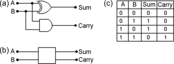 |
| Figure 10.9 (a) A half-adder circuit, with (b) symbol and (c) truth table |
This half-adder is such a useful circuit that it is made in IC form in its own right, and it can, in turn, be used to create other circuits. The name ‘half-adder’ arises because it can be used only as a first stage in an adder circuit. If we need to add only two bits, the half-adder is sufficient, but if we need to add, say, eight pairs of bits, as when we add two bytes, then the other adders will have three inputs: the bits that are to be added plus the carry bit from the previous stage. For example, adding 1011 and 0011 can use a half-adder for the lowest order pair, giving a 0 output and a carry bit. The addition of the next bits is 1
+
1
+
1, because of the carry, and this gives a 1 output and a 1 carry. The next addition uses the carry from the previous stage, and the last addition uses no carry:
| Carry | 0 | 1 | 1 | 0 |
| A | 1 | 0 | 1 | 1 |
| B | 0 | 0 | 1 | 1 |
| Sum | 1 | 1 | 1 | 0 |
If we have the half-adder in IC form, we can connect two half-adders along with an OR gate to provide a full adder, which allows a carry input as well as a carry output. Figure 10.10 shows the circuit, its truth table, and the block representation.
Note
Note
A full adder can be used as a half-adder if the carry input is connected permanently to the 0 voltage level.
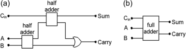 |
| Figure 10.10 (a) The full adder constructed from gates and (b) its symbol |
In practice, adders can be serial or parallel. A serial adder works on each pair of bits (and any carry) at a time, adding the figures much as we do with pencil and paper. The only complication is the need to store the bits, and we shall see how this is done in Chapter 11. A parallel adder will have as many inputs as there are bits to add, and the outputs will appear as soon as the inputs are present. This is very much faster, and though the circuit is more complicated, this is no problem when it can be obtained in IC form.
Figure 10.11 shows what is involved in a typical parallel adder circuit for two 4-bit binary numbers. In this circuit, all of the inputs are applied at the same time, and the only delay is due to the carry bits, because the addition at each of the later stages is not complete until the carry bit has been generated at the previous stage. This typically takes a few nanoseconds per stage, and the process of passing the carry bit from stage to stage is called
rippling through.
Note
Note
Since there is never a carry input at the least significant stage, this could use a half-adder, but when the circuit is constructed in IC form a full adder with the first carry set to zero is normally used.
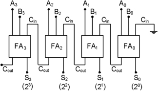 |
| Figure 10.11 A 4-bit parallel adder for two binary numbers |
Subtraction
Definition
The rules for binary subtraction are:
where the −1 entry represents a borrow (or carry-back) action from the next higher bit, rather than the carry-forward operation that is used for addition.
0 − 0
=
0
0 − 1
=
−1 (borrow 1)
1 − 0
=
1
1 − 1
=
0
Figure 10.12 shows how a half-subtractor circuit can be constructed using a NOT gate added to the simple half-adder circuit. Once again, the ‘half’ reminds you that this circuit does not provide for a borrow, and a two-bit full subtractor circuit can be made using half-subtractors as shown in Figure 10.13. A single stage like this can be used for serial subtraction.
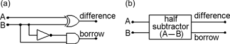 |
| Figure 10.12 (a) The half-subtractor in gate form and (b) as a symbol |
 |
| Figure 10.13 (a) The full subtractor in gate form and (b) as a symbol |
As you might expect, a full subtractor can be made in parallel form, and an example which provides for two 4-bit numbers is illustrated in Figure 10.14 using full subtractor units. This, however, can also be built using full adder circuits, using a method of subtraction that we need not worry about at the moment (twos complement with end-around carry). The point is that it allows subtractors to be made using the same IC components as adders, making production more economical.
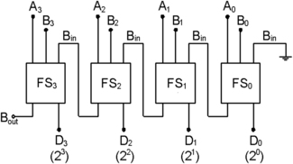 |
| Figure 10.14 A 4-bit full parallel subtractor |
Multiplication and Division
Definition
The rules of binary multiplication are:
and the rules for division are:
There are only two division rules, because division by zero is meaningless.
0
×
0
=
0
0
×
1
=
0
1
×
0
=
0
1
×
1
=
1
0
÷
1
=
0
1
÷
1
=
1
Multiplication and division cannot be carried out by gates alone, because they must be done stage by stage. Consider, for example, a multiplication carried out in the same way as we would multiply two denary numbers:
| 1101 |
| 1010 |
| 0000 |
| 1101. |
| 0000.. |
| 1101... |
| 10000010 |
This starts by multiplying each bit in the upper number by the lowest order bit in the second number, producing in this example a set of zeros. Each bit in the second number (the multiplier) will result in a set of 4 bits (in this example) for the result, and each successive set is shifted left by one place. This action of storage and shifting requires the use of
registers (see Chapter 11), and this is followed by an addition, in this case of four 4-bit numbers, to find the final result, which may contain a carry to an extra bit position.
Division requires the same types of actions and follows the methods used for long division of denary numbers (once familiar to eight-year-olds, but now a lost art in schools). Just as well we can assemble arithmetic circuits that are ready-made for us.
Summary
Summary
Arithmetic can be carried out using gates. The simpler addition and subtraction actions can be carried out using only gates, but the actions of multiplication and subtraction require storage and shifting and are dealt with using
registers. These actions can be used in serial form (repeating the action for each position in a binary number) or in parallel form (with as many arithmetic units as there are bits in the binary numbers).
Code Changing
The need to use codes for digital information often leads to problems in transmitting the digital signals, because we very often cannot provide a signal line for each code signal. Suppose, for example, that we have a set of eight switches, any one of which can be ON (1) or OFF (0), but not allowing more than one switch to be ON at a time. Suppose also that we need to pass this information to some unit which might be a controller or some type of recorder. One obvious method is to use eight lines, one for each switch. A less obvious method is to use the binary numbers for 0 to 7 (a total of eight codes), which cover the range 000 to 111, using only three lines. A circuit that carries out this change from using eight lines to using three lines is called an 8 to 3
encoder. Encoders are used to reduce the number of signal channels needed for data.
Note
Definition
Note
The word
multiplexer is often used interchangeably with
encoder, though strictly speaking the two are not identical. The opposite actions are carried out by the
decoder or
demultiplexer.
Definition
An encoder is used to convert a set of 2
n signal lines, on which only one line at a time can be at logic 1, into binary signals on
n lines. A decoder performs the conversion from
n lines of binary signals to 2
n lines, of which only one at a time can be at logic 1. A multiplexer (
Mux) is used to select one signal from signals on
n input lines and produce the selected signal as an output on one line. A demultiplexer (
Demux) has a single input which varies with time, and will provide outputs on
n lines.
Figure 10.15 shows an encoder block and truth table for the example of eight to three transformation. A decoder for three lines to eight, also shown here, would work in the opposite way, with a 3-bit binary input and a set of eight lines out, only one of which could be at level 1 for each combination of input bits. You might, for example, use the outputs from the decoder to operate warning lights, if only one at a time needed to be illuminated.
Definition
Definition
For any decoder, the binary number input is often referred to as an
address number. This name crops up again when we look at computer circuits.
 |
| Figure 10.15 (a) Encoder and (b) decoder in block form. The illustration shows 8 to 3 encoding and 3 to 8 decoding |
An encoder is needed when each of a set of inputs must generate a unique code pattern. For example, imagine a set of 16 keys (a
hexadecimal keypad) for which each of the 16 input key characters must generate a unique 4-bit output code; we assume that only one key is pressed at a time. This encoder would require 16 inputs, only one of which is selected at any one time, and would provide four output lines to provide the parallel bit pattern. If we needed to reconstitute the pattern of lines at the input, we would use a decoder that would have four input lines and would use the bits on these lines to select one and only one of 16 output characters.
Encoders and decoders can be made using gates, and Figure 10.16 shows an example of a 2 to 4 line decoder using inverters and AND gates, along with a truth-table analysis of the action.
 |
| Figure 10.16 A decoder in gate form for 2 to 4 decoding |
Now let’s look at a multiplexer. Figure 10.17 shows in block form what a 4 to 1 multiplexer is expected to do. There are four data inputs, two address inputs, and a strobe input. The address inputs are used to select one of the four data lines, using an encoding action (which is why encoders and multiplexers are often taken to be almost identical). The data on the selected line is transferred to the single output line when the signal on the strobe line is low (logic 0). This allows all of the data to be sent down one line, a bit at a time, by establishing an address number, pulsing the strobe input, and repeating this for another address number until you have cycled through all the address numbers.
Definition
Note
Definition
A strobe pulse is one that is applied at a set time to allow an action to be carried out. The name was originally used in radar to mean a pulse that was used to enable the receiver for a time that excluded return pulses from nearby targets.
Note
This type of action, allowing a mass of data to be selected for transmission down a single line, is called
time-division multiplexing. The use of a carrier modulated in more than one way (such as the color television sub-carrier) is another form of multiplexing. Multiplexing of the time-division type is very important for digital television and radio, enabling several programs to share a single bandwidth channel.
 |
| Figure 10.17 A multiplexer in block form, in this example a 4 to 1 Mux with two address lines and a strobe line |
Figure 10.18 shows a gate circuit that can carry out the action of multiplexing a set of four inputs. For four inputs, a 2-bit address number is needed to select which input will be connected to the output line when the strobe input goes to logic 0. The opposite action of a demultiplexer is shown in block form in Figure 10.19. There is a single data input and a strobe input, along with the address inputs, in this case using two lines for the addresses of four output lines. Once again, the data on the input line will appear at the selected output line when the strobe pulse voltage is low, and the truth table is in Figure 10.19 with the selected output data line in this example taking the logic value of 0 (the same as the data line input) when the strobe appears (assuming that strobing occurs when the strobe input is low).
Summary
Summary
Encoders, decoders, multiplexers, and demultiplexers are used to change the way that digital codes are carried. Usually, one of the codes will be 8-4-2-1 binary. The distinguishing feature of the multiplexer is that it allows any number of input lines to be used to place signals on a single output line, controlled by a selection address number and an enabling strobe pulse. The demultiplexer carries out the opposite action, assuming that the strobe pulses are correctly synchronized.
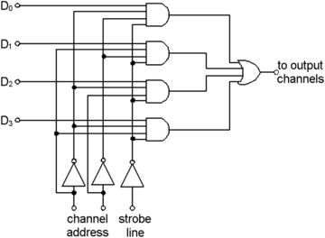 |
| Figure 10.18 A 4 to 1 multiplexer in gate form |
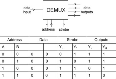 |
| Figure 10.19 Block for a 1 to 4 demultiplexer |
..................Content has been hidden....................
You can't read the all page of ebook, please click here login for view all page.