Chapter 3. Active Components and Integrated Circuits
Transistors. Use of semiconducting crystals. Bipolar and field-effect types. Emitter, collector and base. Control of collector current by base current. Current gain. Bias methods. Use as a voltage amplifier. Use of a load resistor. Bias circuits. Wave inversion in a simple voltage amplifier. Analog linear circuits. NPN and PNP BJTs. Field effect transistors (FETs). MOSFETs. Source, drain and gate electrodes. Dissipation in linear amplifier circuits. Switching use of transistors. Low dissipation in switching circuits. ICs. Circuit on a silicon chip. Effect on reliability. Linear ICs. Opamp. Typical opamp circuits. Dissipation in an opamp. Digital ICs. Logic actions. Combinational logic defined. Sequential actions. Pocket calculators. Scale of integration. Gates. Microprocessors. Universal logic circuit. Programming signals setting current paths.
Transistors
Modern active components are all based on
transistors, which were invented in 1948 by Brittain, Bardeen, and Shockley. Before transistors came into extensive use, the main active components for electronic circuits were vacuum tubes (called
valves in the UK), and these are still used for high-power transmitters. There are two main types of transistors, called
bipolar transistors and
field-effect transistors (FETs), and since the bipolar type came first into use, we will start with that. Most modern electronics systems now, however, are based on the FET, usually in integrated circuit (
IC) form.
The transistor is a component that is created using a semiconductor crystal, and in a sense it is the inevitable result of the use of crystals in radio reception in the 1920s, because this started a line of research into crystal behavior which led to the transistor, even though the materials are quite different.
Note
Definition
Note
It also had the much less desirable effect of starting a cult for imagining that crystals had psychic powers, showing that superstition and ignorance will latch on to anything to promote their nonsense.
Definition
A transistor is a semiconductor component with three terminals. An input between two of the terminals can alter the amount of current flowing to or from the third terminal.
This book is about electronics fundamentals, so that the way in which the transistor works is beyond our scope, but we are interested in what the transistor is and what it does. The symbol that is used on circuit diagrams for a bipolar transistor is a useful reminder (Figure 3.1). This shows three connections, labeled as
emitter,
collector, and
base, with an arrowhead on the emitter lead that points in the (conventional plus to minus) direction of current.
 |
| Figure 3.1 The circuit symbol for a transistor, in this case the NPN type which will pass current when both collector and base are at a positive voltage compared to the emitter |
For the type of transistor (known as NPN) that is illustrated in Figure 3.1, a steady voltage can be connected, with the positive end on the collector lead and the negative (earth) end on the emitter. No current passes, and the same would be true if the voltages were reversed, so that in this state the transistor behaves like an insulator.
With the collector positive and the emitter negative, if the base connection is now slowly made more positive than the emitter, a very small current will eventually pass between the base and the emitter. This pair of connections, emitter and base, is a diode. What is much more significant, however, is that when a small current passes between the base terminal and the emitter terminal, a much larger current will pass between the collector and the emitter. By much larger, I mean anything from 30 to 1000 (or more) times greater. The action is that a very small amount of current passing between base and emitter can control a much larger current passing between the collector and the emitter.
Note
Note
The name transistor comes from
transfer resistor, the original name for the device. The abbreviation
BJT (bipolar junction transistor) is also used now, and is preferable because it distinguishes this type of transistor from the field-effect type that we shall look at later.
Suppose now that we use a resistor connected to a steady voltage to pass a very small steady current through the base. This will, as we have seen, make a much larger current flow through the collector to the emitter. The transistor is acting as a steady-current amplifier, making a large copy of a small current. If now we connect a signal waveform between the base and the emitter, this will cause the current in the base to fluctuate. The current in the collector circuit will also fluctuate, but with a much larger amplitude. For example, a current fluctuation of 1 microamp in the base circuit might cause a fluctuation of 1 milliamp in the collector circuit, a
current gain of 1000 times.
The transistor is now acting as a signal current
amplifier. The steady current passing between base and emitter is called the base
bias current. If we did not use this bias current, the base would not pass current until the input wave voltage reached about +0.56
V, so it could not have any amplifying effect on waves of small amplitude. With enough bias to allow current to flow, the transistor is a very effective amplifier for small signal inputs.
We can also make the transistor act as a
voltage amplifier. The simplest (and least satisfactory) circuit is shown in Figure 3.2. A resistor is connected as a
load between the collector and the positive supply terminal – nothing wrong with that because it is a normal way of converting a current signal into a voltage signal. A much larger value of resistor is connected between the base and the positive supply so that a small steady current flows through the base. Now if we add an alternating signal input at the base, taking care that the input is never so large that it causes the current to stop (by opposing the steady current), then the output will be a much larger voltage output.
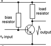 |
| Figure 3.2 The simplest (and least satisfactory) form of transistor amplifier circuit, showing input and output waveforms. The output wave is inverted compared to the input and is of greater amplitude |
This needs some thought. Imagine that the positive peak of the input wave has increased the base current. This will increase the collector current, and because there is more current through the load resistor the voltage across the resistor will be greater. Because there is more voltage across the resistor there is
less between the collector and the emitter, so that the output wave is at its lowest, its negative peak. The output wave is a mirror image of the input, an inverted wave, as is indicated in the drawing.
The snag is that the bias current of this arrangement will not remain constant. A large value of resistance is needed (because the current needed at the base is very small) and even the smallest changes in the resistance or of the gain of the transistor (due to temperature changes) can make a large change to the bias. A much more practical circuit is illustrated in Figure 3.3, using two resistors to set a constant voltage at the base and another resistor in the emitter connection to stabilize the current.
Summary
Summary
A transistor of the bipolar type (BJT) has three terminals: base, emitter, and collector. A small current passing between base and emitter will cause a large current to pass between collector and emitter, with both base and collector positive in this example (NPN transistor). This current gain effect can be used to construct a voltage amplifier in which the output is an amplified and inverted version of the input.
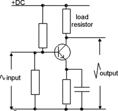 |
| Figure 3.3 The more usual form of a single transistor amplifier. The use of additional resistors stabilizes the steady currents that flow through the transistor |
This principle of using a transistor and a load is at the heart of most of the electronic circuits (called
analog or
linear circuits) that we were familiar with before digital circuits appeared. Transistors are even better suited to digital circuits, as we shall see in Chapter 9 and Chapter 10. The snag about using transistors for amplification is that the output is never a perfect copy of the input (though the imperfections can be made to be very small). A graph of the signal voltage output against the signal voltage input is not a straight line so that this is not a perfectly linear amplifier. There are ways of improving this situation, which will be discussed in the following chapter. The ultimate solution is to use digital signals, and we will look at that later.
NPN and PNP Transistors
Bipolar transistors can come in two forms, called
NPN and
PNP. These P and N letterings indicate the type of carrier that takes most of the current in each region, with N meaning electrons as carriers and P meaning holes as carriers. The NPN transistor conducts mainly by movement of electrons in the collector and emitter and mainly by using holes in the base region. The practical effect is that the NPN transistor is used with a positive supply to both the base and the collector; the PNP transistor is used with a negative supply to both base and collector. Many circuits use a combination of PNP and NPN transistors.
Field-Effect Transistors
FETs have been available for almost as long a time as the bipolar type, but they were not extensively used until later. Nowadays, the field-effect type is used to a much greater extent (in ICs; see later) than the bipolar type, and the most important field-effect type is the metal-oxide-semiconductor field-effect transistor, abbreviated to MOSFET.
The MOSFET uses quite different principles. Current can pass between two terminals called the
source and
drain, and this current is controlled by the
voltage (not current) on a third terminal, the
gate. On a circuit diagram, the MOSFET is indicated as shown in Figure 3.4 and the important point about it is that there is no current passing to or from the gate for either positive or negative bias.
 |
| Figure 3.4 The symbol for a metal-oxide-semiconductor field-effect transistor (MOSFET), in this case the type called a p-channel MOSFET |
This type of transistor needs a voltage signal only, not a current signal, so that the power needed at the input is very much smaller than is needed for a bipolar transistor, almost a negligible amount. Depending on the design of the MOSFET, a bias voltage can be used or the MOSFET can be operated without bias. A typical amplifier circuit is illustrated in Figure 3.5.
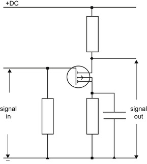 |
| Figure 3.5 A typical metal-oxide-semiconductor field-effect transistor (MOSFET) amplifier circuit |
MOSFETs do not provide as much amplification (voltage gain) as bipolar transistors, and their uses were at one time predominantly for digital IC circuits (see later). Specialized types of MOSFETs are now used in audio amplifiers and in tuning circuits for FM radios.
Note
Summary
Note
There are various varieties of MOSFET, such as PMOS, NMOS, and CMOS, all of which are used extensively in digital circuits. The differences are not important at this stage. The MOSFET is sometimes known as IGFET, with IG meaning
insulated gate.
Summary
The MOSFET is a form of field-effect transistor which has become the most commonly used type of transistor. There are three terminals, called source, gate, and drain, with the voltage on the gate controlling the current between the source and the drain. The current flowing in the gate is almost immeasurably small. An amplifier circuit uses a load resistor connected to the drain, and a voltage bias supply to the gate if needed.
Switching
The analog uses of transistors, BJT or MOSFET, for amplifier circuits require the designer to set the correct bias, and use circuits that will provide the nearest approximation to a straight-line graph of output plotted against input. These amplifier circuits all cause the transistor to dissipate power, because the optimum bias is usually with the collector or drain voltage set to about half of the steady voltage supply, and passing a current that is about the amount that needs to be supplied. For example, if the DC supply is at 12
V and a current of 50
mA needs to be supplied, then the transistor will be biased to a collector or drain voltage of 6
V and a current of about 50
mA. This corresponds to a power dissipation of 6
×
50
mW
=
300
mW. This is typically the maximum that a small transistor can dissipate without overheating.
All linear amplifier circuits suffer from this dissipation problem, and when higher power outputs are needed transistors have to be designed so that they can release their heat through a metal casing, or a metal stud, to metal fins that will dissipate the heat into the air. For a few specialized purposes, water cooling can be used, but air cooling, with or without a fan, is much more common.
There is, however, another way of operating transistors, though it is a long way removed from their use as linear amplifiers. If a transistor of any type is operated without bias, it will not pass current when there is no input signal. With no current flowing, there is no power dissipation, and so no heat to worry about. If a signal at the input (base or gate) now makes the transistor conduct fully, a comparatively large current will pass, but the voltage at the collector or drain will be low (as low as 0.2
V for some types) and the power dissipation will be small.
Note
Note
If we use transistors for working with pulses, then the power dissipation will be very low, particularly if the transistor is switched on for only a short time in each cycle. This switching use of transistors is not suited to linear amplifiers, but it is ideal for digital circuits, as explained in Chapter 10.
Transistor switching circuits can also be devised that make the dissipation even lower. For example, we have assumed so far that the load for a switching transistor will be a resistor, so that power will be dissipated in the resistor whenever current flows. If the load resistor is replaced by another transistor in a switching circuit, the ‘load' transistor can be switched as well, ensuring that its dissipation is also very low.
Summary
Summary
Transistors that are used for analog designs (the amplification of waves as distinct from pulses) are not as linear as we would like, and they dissipate power, risking damage to the transistors. The alternative way of using transistors is as switches, working with pulses that turn the transistor on for brief periods, so that linearity is not important and dissipation can be very low. This method of operation, however, is suited only to digital circuits.
Integrated Circuits
Only a few years after the invention of the bipolar transistor, G.R. Dummer, working at a UK government laboratory, suggested that the processes that were used to manufacture individual transistors could be used also to manufacture resistors, capacitors, and connections on the same piece of semiconductor material, making it possible to produce a complete circuit in one set of operations. Though the mandarins of the UK civil service who read his report attached no significance to it, others did. The USA was desperately trying to improve the reliability of electronic equipment for space use, and Dummer's suggestion was the answer to the problem.
It is possible to make individual electronic components reasonably reliable, but the weak point in large and elaborate circuits is the number of connections that have to be made between components. If you can replace 20 individual components by a single component then, other things being equal, you have made the circuit connections 20 times more reliable, and this is what creating a complete circuit in one set of operations amounts to. In addition, there is nothing that restricts the idea to just 20 components in a circuit, though the pioneers could not have imagined creating circuits with several million components on one small piece (
chip) of silicon. This device is the
integrated circuit or IC. As is the case with most British ideas, we ended up buying into the technology that we had failed to develop for ourselves.
The space race between the USA and the USSR spurred the development of ICs, so that by the 1970s we could buy complete circuits on a single tiny chip of silicon that were vastly more reliable than anything we had ever imagined. These ICs were mainly for digital circuits, though there are also many types of linear (amplifier) ICs. In addition to reliability the advantages of these ICs include low cost, small size, low dissipation, and predictable performance. By this point in the twenty-first century, making connections between individual (
discrete) transistors is an almost forgotten skill used only where circuits are created for special purposes.
Summary
Summary
The IC was originally a British idea, but you could be pardoned for not knowing that because they made nothing of it. The principle is to improve reliability by using the manufacturing methods that are used to create transistors also to make resistors, capacitors, and connections between these components, all on the same tiny chip of silicon that is used to make transistors. These chips are mass produced, and the elimination of external connections makes the reliability of a circuit with a large number of individual components as good as the reliability of a single component. In addition, the cost can be low because of mass production, and the size of a complete circuit is little more than that of a single transistor.
Linear Integrated Circuits
Digital circuits have always accounted for a majority of the ICs that have been manufactured, but there has always been one particularly important type of linear IC, called the operational amplifier (or
opamp). The circuit of an opamp is unimportant to the user, and only the designer is likely to know exactly what goes on inside the chip, so the user of an opamp works from a set of figures that describe its performance. The usual symbol is illustrated in Figure 3.6.
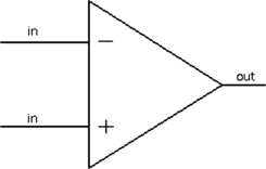 |
| Figure 3.6 The symbol for an operational amplifier. The + and − input markings refer to the phase of input signals, not to the voltage of DC supplies. The DC supplies are usually balanced, typically +12
V and −12
V |
Instead of spending hours on the design of an amplifying circuit, a designer can use an opamp and (typically) two resistors to get the amount of gain that is required, and the calculations are simple. This does not mean that opamps can be used for any task that was formerly carried out by circuits using separate transistors (discrete circuits), but 99% of them would be a reasonable estimate, sufficient to make the opamp a considerable boon.
Note
Note
This is an excellent example of how passive components (resistors in this case) can be used to control the action of an active component (the opamp). Because the amount of gain is set by the passive components, their tolerance and stability are very important.
The typical opamp has two inputs, marked + and −, and one output, and it is used with a balanced pair of DC supplies, typically +12
V and −12
V. The input markings do not refer to + or − supplies, but to the
phase of signals. If you use the + input, the output signal will be in phase with the input signal. If you use the − input, the output signal will be in anti-phase, a mirror-image waveform, like the output from a single-transistor amplifier. For a number of reasons, it is much more usual to take the input signal to the anti-phase (−) input.
Figure 3.7 shows a typical amplifier circuit that will provide a gain of about 47 times. How do we know? Because that is the ratio of values R
1/R
2. The opamp circuit is unknown, but the manufacturer guarantees that the gain of the chip is at least 100,000. The resistor R
1 is connected between the output and the input, so that some of the output is fed back, opposing the input. This reduces the gain, and it also makes the amount of gain depend only on the resistor values, not on anything inside the IC (unless some part of the IC circuit is overloaded). This means an end to complicated calculations and guesswork, and even the arithmetic is simple.
Note
Note
In this example, the DC power supplies have been shown. Opamp circuits are usually shown with all of these power supply connections omitted. The resistor R
3 is used to ensure that the + input is connected to earth, and its precise value is not important.
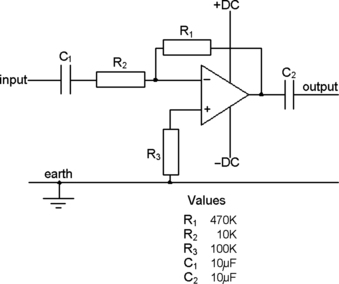 |
| Figure 3.7 A typical opamp circuit in which the gain (amount of amplification) is determined by the values of resistors R
1 and R
2 |
Using an opamp is not an answer to everything, because the circuit might need to work at a frequency higher than the opamp can cope with, but a later type of opamp probably will cope. In addition, there is a host of specialized opamps designed for specific purposes, and catering for almost all the exceptions to the general rules.
There is one serious handicap that affects all opamps. Because an opamp is designed for amplification, the transistors must use bias and therefore dissipate heat. This determines how complicated an opamp can be, in terms of the number of transistors in the circuit, because each transistor will contribute to the heat output and that heat must be transferred to the air if the opamp is not to overheat. The same applies to opamps that are intended to provide a power output to loudspeakers, electric motors, and other devices.
Summary
Summary
The most common type of linear (analog) IC is the operational amplifier or opamp. This has a very high gain value, and is normally used in a circuit in which two external resistors control the gain. In the situations where such an opamp is not suitable, there are other designs that will deliver the performance that is needed for more specialized purposes. The snag is that heat dissipation limits the complexity and power capabilities of an opamp.
Digital Integrated Circuits
Digital ICs are the more common variety, mainly because of the vast number of digital devices (not just computers) that make use of these types of ICs. The transistors inside digital ICs are being used not as amplifiers, but as switches. This means that the heat dissipation for each transistor is very low, allowing digital ICs to be constructed using hundreds, thousands, and even millions of transistors. In addition, heat-dissipating components (resistors) can be designed out because substituting a transistor for a resistor is easy when both use the same techniques (and an IC transistor can be physically smaller than a resistor). Passive components are much less important in digital circuits than in analog circuits.
Definition
Definition
Digital ICs deal with pulse inputs and outputs and use switching actions with very low dissipation.
The simplest digital ICs carry out just one type of switching action, and they can perform the operations that are called
logic actions (Chapter 10). The type of circuits that can be constructed using these ICs would typically be used as controllers for machines, using several inputs to decide whether an output should be on or off.
When should your washing machine start a cycle? Obviously, it is when the main switch is on, a program is selected, the drum contains some clothes, the water supply is switched on, and the main door is closed. The machine must not switch on unless all of these ‘inputs' are present, and this action of providing an output only for some particular set of inputs is typical of the type of circuits we call
combinational. We will come back to all that in Chapter 10. All of the first generation of digital ICs were intended to solve that type of problem, and these ICs are still in production more than 40 years on.
The next development was to make ICs that dealt with
sequential actions, such as counting. These ICs required more transistors in each circuit, and as manufacturing methods improved designers found that they could produce not just the ICs that could be assembled into counters but the complete counters in IC form. At the same time, IC methods were being used to create displays, the LED and LCD displays that are so familiar now, so that all the components that were needed for a pocket calculator were being evolved together, and soon enough a complete calculator could be made using just one chip.
The pocket calculator story is a useful one to trace this part of the history of electronics. The first pocket calculators used several ICs, and they needed a considerable amount of assembly work. You could at that time buy DIY kits if you were curious to find out how the calculator was assembled, and such kits were also cheaper than a complete calculator. Nowadays, the calculator consists of just one IC, and there is practically no assembly. It costs more to assemble and package the components as a kit than to make and package the complete calculator, and costs are so low that the calculators can often be given away as a sales promotion.
Another thread of the story concerns the power required. The first pocket calculators needed four AA cells and gave about one month of use before these were exhausted. Power requirements have been so much reduced that some calculators are likely to be thrown away before the single cell that they use is exhausted, and it is possible to run calculators on the feeble power from a photocell (which converts light energy into electrical energy).
The early digital ICs were constructed using bipolar transistors, mainly because at the time these were easier to construct. The snag with bipolar transistors is that they need current inputs: no current flows between collector and emitter unless a current flows between base and emitter. The base current might be small, but some base current must exist, and so a bipolar transistor must inevitably dissipate more power than the MOSFET type, which needs no current between gate and source terminals.
Eventually, then, digital ICs started to be manufactured using MOSFET methods, and this allowed the number of transistors per IC to be dramatically increased. This packing of transistors was measured roughly by names that we use for
scale of integration. This is described in terms of the number of simple logic circuits (
gates) that can be packed into a chip, and the first ICs were small-scale integration (SSI) devices, meaning that they contained the equivalent of 3–30 logic circuits. The pace of development at that time (the 1960s) was very fast, so that the terms medium-scale integration (MSI) and large-scale integration (LSI) had to be introduced, corresponding to the ranges 30–300 and 300–3000 logic circuits, respectively.
This is a good example of how technology runs ahead of expectation. LSI soon became commonplace, and we had to start using very-large-scale integration (VLSI) for chips with more than 3000 gates per chip. Soon enough, chips containing 20,000 or more gates were being manufactured, but a new label, extra-large-scale integration (ELSI), was not introduced until more than one million gates could be put on a single chip. Scale-of-integration names are not normally used nowadays. Moore's law once predicted that the number of transistors that could be placed on an IC would double each year, dating from the start in 1958. Gordon Moore (founder of Intel) thought in 1965 that this trend would flatten after 10 years, but it holds true at the time of writing in 2010 and may continue as new ways of producing ICs are developed.
Summary
Summary
Digital ICs are classed in terms of the number of simple gate circuits that they replace on average. Modern chips are usually of the VLSI class, equivalent to 20,000 or more gates, and computer ICs are often in the ELSI class, equivalent to one million or more gate circuits.
The Microprocessor
The development of the microprocessor followed logically from the use of digital logic circuits, and this is an introduction only; more details follow in Chapter 13.
The microprocessor is a kind of universal logic circuit. Imagine you have a large number of digital logic ICs. You could make these into circuits, each of which would carry out some sort of control action, depending on how you connected the chips together. You might find that the circuits you used had a lot in common, and that you could make one circuit which used a number of switches, so that by setting switches you could change the overall action from one design to another. The next logical step is to make these switches in the form of transistors, so that the switching can be electrical. It is that this stage that the microprocessor becomes a possibility.
The first microprocessor was designed and built to a US military contract which called for a logic circuit whose action could be controlled by inputs of signals called
programming signals. The military contract was canceled, and the manufacturer (Intel) was left with a large number of devices for which there was no known market. A few enthusiasts found that these chips could be used to make simple computers, and once this became known, a small firm called Altair put together a kit for building these computers. The sales of this kit were phenomenal, and by the end of a year most of the microcomputer firms that we know today were in business. It is ironic to note that larger firms such as IBM dismissed these machines as toys and predicted that they would all disappear inside a year. As it is, the IBM PC business was sold to Lenovo (based in China) in 2004.
Summary
Summary
The microprocessor is a form of universal logic circuit whose action can be set by the user. This allows the microprocessor to replace a vast number of other circuits, and to be more flexible in use, because its action can be modified by programming it, using pulse inputs.
..................Content has been hidden....................
You can't read the all page of ebook, please click here login for view all page.