Chapter 11. Counting and Correcting
Combinational and sequential circuits. The flip-flop type of circuit. S-R flip-flop. Set and Reset actions. J-K type of flip-flop. Clock input. Race hazards. J & K programming inputs. Triggering edge. J-K modes: hold, set, reset, toggle. J-K as counter or frequency divider. Asynchronous and synchronous counters. Counter uses - frequency meter, counter/timer. Digital clocks and watches. Digital voltmeter block diagram. Frequency synthesizer. Phase-locked loop. Voltage-controlled oscillator. Registers. Shifting and rotating action of registers. Latching action. SISO register symbol and circuit. PISO register and SIPO register. SPLD circuits. CPLD. FPGA. ASIC and ASSP chips. SoC (system on a chip). Memory chips. RAM defined. ROM defined. EPROM and EEPROM. Flash memory. Error control and correction of transmitted digital signals. Noise immunity of digital signal. Bit error rate. ARQ system. Forward-error control (FEC). Errors caused by white noise and by impulsive noise. Interpolation methods. Checksums. Hamming codes. Error syndrome. Cyclic redundancy check (CRC). Reed-Solomon coding.
Sequential Circuits
Gate circuits are one basic type of digital circuit, the
combinational circuit. The other basic type of digital circuit is the
sequential type. The output of a sequential circuit, which may mean several different output signals on separate terminals, will depend on the
sequence of inputs to the circuit. One simple example is a counter integrated circuit (IC), in which the state of the outputs will depend on how many pulses have arrived at a single input. Compare this with the combinational (gate) circuit in which there are several inputs and the output depends on the combination of inputs.
The basis of all sequential circuits is a circuit called a
flip-flop, and the simplest flip-flop circuit is called the S-R flip-flop, with the letters S and R meaning set and reset. Though this type of flip-flop is not manufactured in IC form (because it is just as simple to manufacture more complex and more useful types), it illustrates the principle of sequential circuits more clearly than the more complicated types.
Definition
Note
Definition
A flip-flop is a circuit whose output(s) change state for some sequence of inputs and which will remain unchanged until another sequence of inputs is used. Unlike a gate, simply changing the inputs to a sequential circuit does not necessarily change the outputs.
Note
One feature of flip-flops is the use of two outputs, conventionally labeled as
 and Q# (or Q). The Q output is the main output, and the Q# output is the inverse of the Q output.
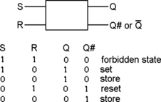
Figure 11.1 shows the block diagram for one variety of simple S-R flip-flop along with a table of inputs and outputs. The notable point is that the table shows five lines, and that the line that uses 0 for both inputs appears twice. The output for S
=
0 and R
=
0 can be either Q
=
1 or Q
=
0, and the value of Q depends on the
sequence that leads to the S
=
0, R
=
0 state. If you use inputs S
=
1, R
=
0, then Q
=
1, and this value will remain at 1 when the input changes to S
=
0 and R
=
0. Similarly, if the inputs are S
=
0, R
=
1, the Q output becomes 0, and this remains at 0 when the inputs change to S
=
0, R
=
0.
Note
Note
One state, with S
=
1 and R
=
1, is forbidden because all the uses for flip-flops require Q# always to be the opposite of Q, and the S-R flip-flop violates this requirement when S
=
1 and R
=
1.
 |
| Figure 11.1 The S-R (or R-S) flip-flop with its state table |
The meanings of S and R are now easier to understand. Using S
=
1 and R
=
0 will
set the output, meaning that Q changes to 1. Using S
=
0, R
=
1 will
reset the output, meaning that Q changes to 0. The input S
=
0, R
=
0 is a storing (or
latching) input, making the flip-flop remain with the output that it had previously. Though the single S-R flip-flop is not manufactured in IC form, it is useful (as a latch, see later) and can be constructed using two NAND gates as shown in Figure 11.2. Multiple S-R latch chips are available.
Summary
Summary
Sequential circuits are the other important digital type, used in counting and for memory actions. The simplest type is the S-R flip-flop (or latch), whose output(s) can be set by one pair of inputs and reset by reversing each input. The output is held unchanged when both input signals are zero. Sequential circuits can be created using gates, emphasizing the importance of the gate as a fundamental digital circuit.
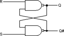 |
| Figure 11.2 How an S-R flip-flop can be constructed using NAND gates. Another version can be made using NOR gates, with a slightly different state table |
The J-K Flip-Flop
Though simpler types exist, the most important type of flip-flop is that known as the master–slave J-K flip-flop, abbreviated to J-K. This is a
clocked circuit, meaning that the action of the IC is carried out only when a pulse is applied to an input labeled
clock. This is the type of flip-flop that is most commonly manufactured in IC form because it can be used in place of so many other flip-flops.
Using this type of flip-flop allows the actions of a number of such circuits to be perfectly synchronized, and it also avoids the kind of problems that can arise in some types of gate circuits when pulses arrive at slightly different times. These problems are called
race hazards, and their effect can be to cause erratic behavior when a circuit is operated at high speeds. When clocking is used, the circuits can be operated
synchronously, meaning that each change takes place at the time of the clock pulse, and there should be no race hazards.
The J-K flip-flop uses three main inputs, labeled J, K, and clock (Ck). Of these, the J and the K are
programming inputs whose voltage levels will control the action of the flip-flop at the time when the clock pulse triggers the circuit. Because there are two programming inputs, and each of them can be at either of two levels (0 or 1), there are four possible modes of operation of the J-K flip-flop.
We can describe each of those modes of action in terms of what voltage changes occur at the output when the clock-pulse edge arrives. The usual
triggering edge is the trailing back edge, the level 1 to level 0 transition of a pulse, and in Table 11.1, the condition of the Q output before the arrival of trailing edge is indicated as Q
n and the condition after the edge as Q
n+1.
The input for this table is the clock pulse, with the J and K terminals used for programming, and outputs are taken from the Q and Q# terminals. Remember that the Q# output is
always the inverse of the Q output. In older texts this is often shown by drawing a bar over the Q. The table shows the possible states of inputs before and after the clock pulse, showing how the voltages on the J and K pins will determine what the outputs will be after each clock pulse.
The four modes which are indicated in Table 11.1 are as follows.
• The
hold mode. With J
=
0 and K
=
0, the output is unchanged by clock pulses. This avoids the need for further gating if you want to keep the flip-flop isolated.
• The
set mode, with J
=
1, K
=
0. Whatever the state of the outputs are before the clock pulse edge, Q will be set (to 1) at the triggering edge and will stay that way.
• The
reset mode, with J
=
0, K
=
1. Whatever the state of the outputs before the triggering edge, Q will be reset (to 0) at the edge and will stay that way.
• The
toggle mode, with J
=
1, K
=
1. The output will change over each time the circuit is clocked.
In addition to the inputs J and K, which affect what happens when a clock pulse comes along, these flip-flops are usually equipped with S and R terminals, which are also called preset (Pr) and reset (R) terminals. These will affect the Q and Q# outputs of the flip-flop immediately, irrespective of the clock pulses. For example, applying a zero input to the R input will reset the flip-flop whether there is a clock pulse acting or not. This action is particularly useful for counters that have to be reset so as to start a new count.
Summary
Summary
The J-K flip-flop uses two programming inputs labeled J and K, whose voltages determine how the flip-flop will operate when a clock pulse is applied. One particularly useful input is J
=
1, K
=
1, which allows the flip-flop to reverse (or
toggle) the output state at each clock pulse, so that its output is at half the pulse rate of the clock. Two inputs labeled S and R (or Pr and R) allow the output to be set (preset) or reset independently of the clock pulses.
The use of two programming inputs, J and K, therefore causes a much more extensive range of actions to be available. Note that if both the J and K terminals are kept at level 1, the flip-flop will toggle so that the output changes over at each clock pulse, as is required for a simple binary counter (Figure 11.3).
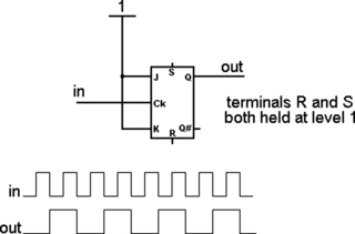 |
| Figure 11.3 Using a J-K flip-flop as a counter or frequency divider |
Flip-flops are the basis of all counter circuits, because the toggling flip-flop is a single-stage scale-of-two counter, giving a complete pulse at an output for each two pulses in at the clock terminal. By connecting another identical toggling flip-flop so that the output of the first flip-flop is used as the clock pulse of the second, a two-stage counter is created, so that the voltages at the Q outputs follow the binary count from 0 to 3, as Figure 11.4 shows. This principle can be extended to as many stages as is needed, and extended counters of this type can be used as timers, counting down a clock pulse which can initially be at a high frequency.
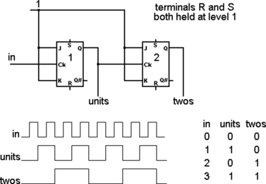 |
| Figure 11.4 A two-stage simple counter using J-K flip-flops |
The type of counter that uses toggling flip-flops in this way is called
asynchronous, because the clock inputs to the flip-flops do not occur at the same time and the last flip-flop in a chain like this cannot be clocked until each other flip-flop in the chain has changed. For some purposes, this is acceptable, but for many other purposes it is essential to avoid these delays by using
synchronous counter circuits in which the same input clock pulse is applied to all of the flip-flops in the chain, and correct counting is assured by connecting the J and K terminals through gates. Circuits of this type are beyond the scope of this book, and details can be found in any good text of digital circuit techniques. In this book we shall, as usual, concentrate on block diagrams which are not concerned with whether a counter is synchronous or not.
Summary
Summary
The toggling flip-flop is the basis of all counter circuits, which use the clock as an input and the Q outputs as the outputs. In such a circuit, the Q outputs provide a binary number which represents the number of complete clock pulses since the counter was reset.
Counter Uses
Apart from their obvious applications to clocks and watches, counters are used extensively in electronics, and particularly in modern measuring instruments. ICs exist to provide for measurement of all the common quantities such as direct current (DC) voltage, signal peak and root mean square (RMS) amplitude, and frequency, using counting methods. Most of the modern ICs of this type provide for digital representation, so that the outputs are in a form suitable for feeding to digital displays. The simplest application of counters to instruments is for frequency measurement.
Frequency Meter
A frequency meter makes use of a high-stability oscillator, normally crystal controlled, to provide clock pulses. In its simplest form, the block diagram is as shown in Figure 11.5, with the unknown frequency used to open a gate for the clock pulses. The number of clock pulses passing through the gate in the time of one cycle of the input will provide a measure of the input frequency as a fraction of the clock rate. For example, if the clock rate is 10
MHz and 25 pulses of the unknown frequency pass the gate, then the input frequency is 10/25
MHz, which is 400
kHz. A counter circuit can find the number and display it in terms of the clock frequency to give a direct reading of the input frequency.
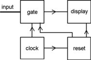 |
| Figure 11.5 Simplified block diagram for a frequency meter |
In this simple form, the frequency meter could not cope with input frequencies that are greater than the clock rate, nor with input frequencies that would be irregular sub-multiples. For example, it cannot cope with 3.7 gated pulses in the time of a clock cycle. Both of these problems can be solved by more advanced designs. The problem of high frequencies can be tackled by using a switch for the master frequencies that allows harmonics for the crystal oscillator to be used. The problem of difficult multiples can be solved by counting both the master clock pulses and the input pulses, and operating the gate only when an input pulse and a clock pulse coincide. The frequency can then be found using the ratio of the number of clock pulses to the number of input pulses.
Suppose, for example, that the gate opened for 7 input pulses and in this time passed 24 clock pulses at 10
MHz. The unknown frequency is then 10
×
7/24
MHz, which is 2.9166
MHz. Frequency meters can be as precise as their master clock, so that the crystal control of the master oscillator determines the precision of measurements.
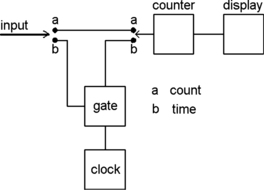
Counter/Timer
A counter/timer is used for the dual roles of counting pulses and measuring the time between pulses, and Figure 11.6 shows the block diagram, omitting reset and synchronizing arrangements.
 |
| Figure 11.6 Block diagram for a counter/timer instrument |
The counter portion is a binary counter of as many stages as will be required for the maximum count value. The input to the counter is switched, and in the counting position, the input pulses operate the counter directly. When the switch is changed over to the timing position, the input pulses are used to gate clock pulses, and it is the clock pulses that are counted. In a practical circuit, the display would be changed over by the same switch so as to read time rather than count.
The timer action is obviously applied to digital watches and clocks. For both watch and clock applications the frequency of vibration of the quartz crystal will be around 32
kHz and this is counted down to suit the display, driving either a liquid crystal display (LCD) unit or a miniature motor to give 1
s impulses to a gear-train so as to make use of the traditional second, minute, and hour hand display. For a watch, the size of the electronics unit is all important, particularly for ladies’ watches, but larger watches and clocks have more space to play with. Watches are also limited for battery power, and the miniature button cells have a life that depends on the watch design, some providing five years or more.
A recent trend in both watches and clocks is synchronization from master signals such as the MSF Rugby time signals (now sent out from a transmitter in Cumbria). The US equivalent is station WWVB. The master clock at Rugby (similar to others around the world) uses the vibration of the caesium-133 atom as a time standard. The natural frequency is 9.192631770
GHz, and its precision is ±1
second per million years. The signal is transmitted at a more modest frequency of 60
kHz and it carries coded information on month, day of month, day of week, hour, minute, and second, with additional codes that control the changes to and from summer time.
Note
Note
MSF is not a technical abbreviation; it was the old call-sign for the Rugby radio transmitter which was built in 1923, using an antenna of about 43
km of copper cable (and 190
km of copper wire used as an earth connection).
Watches such as the Casio Waveceptor conserve battery power by switching on the MSF detector at one or more times in the night for long enough to download the information. Battery power is further conserved by moving the minute hand every 20
s rather than continually, so that battery life of five years or more can be obtained. Larger units in clocks can use AA cells and keep a continuous reception of MSF, along with a continuously moving second hand with gearing to provide minutes and hours.
The most useful feature of these units is that they can automatically respond to the hour advance in spring and the reverse action in autumn. The watches have the disadvantage of the older digital watches that they have to be controlled by buttons, and advancing or retarding the display on a flight can be a fiddly business.
Summary
Summary
Frequency meters and counter/timer circuits are obvious applications of counter circuits to measuring devices, and they have completely replaced older methods. The most familiar applications of timers are in quartz watches and clocks.
Digital Voltmeter Basics
At one time, all voltmeters were of the analog type. The voltage that was to be measured was used to pass current through a resistor of precise and known values, and the current passing was measured by a meter. The meter scale was calibrated in terms of volts, so that the reading was direct; it did not require any calculations. The problem with this type of meter is that it takes a current from the circuit, so that it alters, even if only slightly, the voltage that it is measuring. Another point is that the instrument is fragile, depending on a delicate meter movement. Modern digital meters take a negligible current and present the results as a number rather than as a scale reading. They are also more robust.
The most common IC of this type is the digital DC voltmeter IC, and a brief account of its action provides some idea of the operating principles of many instrumentation ICs.
Referring to the block diagram of Figure 11.7, the voltmeter contains a precision oscillator that provides a master pulse frequency. The pulses from this oscillator are controlled by a gate circuit, and can be connected to a counter. At the same time, the pulses are passed to an integrator circuit that will provide a steadily rising voltage from the pulses.
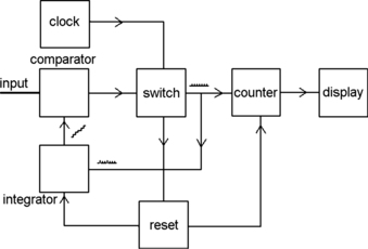 |
| Figure 11.7 Block diagram for a digital voltmeter. The block is for the main measuring unit, neglecting resistors that are used to extend the range for larger voltages |
When this rising voltage matches the input voltage exactly, the gate circuit is closed, and the count number on the display then represents the voltage level. For example, if the clock frequency were 1
kHz, then 1000 pulses could be used to represent 1
V and the resolution of the meter would be 1 part in 1000, though it would take 1
s to read 1
V. After a short interval, usually around 0.25
s (determined by using another clock or a divider from the main clock) the integrator and the counter are reset and the measurement is repeated. Complete meter modules can be bought in IC form, using fast clock rates and with the repetition action built in.
Summary
Summary
The digital voltmeter is a less obvious use of counters in measurement, and its action depends on the use of a very precise integrator in IC form to produce a sawtooth voltage waveform from a set of counted pulses. Digital voltmeters have almost completely replaced the older analog type (which now turn up at antiques fairs).
A very different application of digital methods is illustrated in Figure 11.8, which shows a
frequency synthesizer such as was used on analog television receivers and in a simpler version for frequency-modulated (FM) receivers as a local oscillator for the superhet action. This, strangely enough, depends for its action on an
analog circuit called a
phase-locked loop (PLL), which compares the phases of two input signals of about the same frequency and whose output is a voltage whose size depends on the amount of phase difference between the input signals. If the input frequencies are different the output of the PLL is not a steady voltage, but if the frequencies are identical but with a phase difference, then the PLL output is a steady voltage.
 |
| Figure 11.8 A frequency synthesizer form of oscillator as used for television tuners |
The reference oscillator uses a crystal control and is precise enough to maintain a frequency as constant as any of the transmitted carriers. Its frequency is typically 3
MHz, which allows the use of comparatively low-cost components. This 3
MHz frequency is divided by a factor of 1536 to give 1953.125 Hz, and this frequency is used as one input to the PLL. Another oscillator, labeled VCO (voltage-controlled oscillator), is used as the local oscillator for the television receiver, and will be working at an ultrahigh frequency (UHF), such as 670.75
MHz.
The point of using the VCO is that its operating frequency can be altered by applying a steady input voltage, replacing any form of mechanical tuning. This oscillator frequency is divided by a fixed factor of 64 to give 10.480468
MHz, and this frequency is then used as the input of a programmable divider, whose division ratio can be anything from 256 to 8191. The numbers that control these division ratios are obtained from a memory within the tuner, and this is programmed with control number for each possible channel when the receiver is first set up. This system allows tuning to be much less affected by low signal strength, so that a radio with a digital tuner can be used where an older type would not lock on to a signal.
For example, if the frequency of 10.480468
MHz is divided by 5366, the result is 1953.125
Hz, which is identical to the frequency from the crystal-controlled oscillator. If the VCO frequency changes slightly, the frequencies into the PLL will no longer be equal, and a voltage will be generated from the PLL and used to correct the VCO. If you want to change channels, you press a switch that alters the divider ratio, causing a change in the PLL output that will then alter the frequency of the VCO until the new channel is perfectly tuned. This is all a long way from the variable-capacitor tuning of the early radios.
Summary
Summary
Frequency synthesizers are another application of counter circuits, and this type of action is now extensively used in radio and television receivers to produce the correct oscillator frequency for a superhet receiver circuit. This type of tuning is better able to use remote control and push-button selection actions, and has completely replaced the old-style rotating-knob tuning for television receivers, and FM or digital radio receivers.
Registers
Definition
The use of flip-flops in binary counters is just one application of these versatile building-blocks. A register, usually found in integrated form, is another method of using flip-flops for storage of binary digits and for logic operations that are called
shifting and
rotating.
A register is created from a set of flip-flops connected together, and there are four basic methods which are distinguished by the initials of their names. The simplest type is called parallel in, parallel out (PIPO), and a register of this type has no connections between the flip-flops (Figure 11.9).
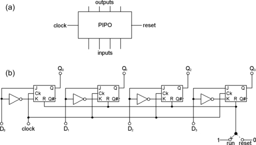 |
| Figure 11.9 The PIPO register, showing (a) the symbol and (b) a circuit using flip-flops |
Each flip-flop of this type of register has an input and an output, and the principle is that the inputs will determine the state of the outputs, and these outputs will be maintained until another set of input signals is used to change them. This type of register is used for storage, because each flip-flop is storing a bit (0 or 1) and will hold this bit until new input signals are used or until the power is switched off. This system was at one time used for computer memory, but it requires too much power (because each flip-flop draws current whether it is storing 1 or 0) for modern systems. The system, also called static random access memory (SRAM), is still used for small, fast memories.
The use of a register for very short-term storage is called
latching. For example, using a latch register allows a set of digits that may exist for only one clock cycle (the time between two clock pulses) to be viewed on a display for as long as is needed. This facility is particularly useful for measuring instruments in which the signals may change rapidly but the display must remain static for long enough to be read. A timer, for example, would be of little use if the time, measured in units of milliseconds, was displayed directly as the counter output, because the display on the least significant digits would be constantly changing and would not be readable until the timer stopped.
It is better to use a register as a latch between the counter and the display so that the time can be displayed without stopping the counter. This also allows intermediate times to be displayed. We can, for example, display the time for one lap of a race, while allowing the counter to continue timing the rest of the race. A latching action is also an essential part of a modern digital voltmeter (using designs more modern than the illustration in Figure 11.7), providing a steady reading (which is updated once per second) even when the voltage level is fluctuating slightly.
Summary
Summary
A register is a circuit that uses a set of flip-flops. The simplest type is the parallel in, parallel out register (PIPO) or latch, in which the flip-flops are independent (apart from a reset line), each with an input and an output. The action is used mainly for storing the bits of a digital signal, so that the register must use as many flip-flops as there are bits in the stored signal.
The opposite type of register is titled serial in, serial out (SISO). Each flip-flop has its output connected to the input of the next flip-flop in line (Figure 11.10), so that the whole register has just one input and one output. This is used as a signal delay and as a counter. On each clock pulse input, the bits in the flip-flops are shifted, meaning that they cause the next flip-flop in line to change. For a set of four flip-flops this will cause the waveforms to appear as shown in Figure 11.11. If there are no connections to the intermediate flip-flop outputs, this register acts as a divide-by-four or count to four circuit.
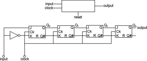 |
| Figure 11.10 The SISO register with symbol and a circuit using flip-flops |
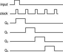 |
| Figure 11.11 The result of using a square pulse input for the first of a set of clock pulses. The pulse is cycled through the register by one stage on each clock pulse |
The parallel in, serial out (PISO) register is used mainly to convert parallel signals on a set of lines into a serial signal on one line. A set of bits on the input lines will affect each flip-flop in the register. By pulsing the clock line once for each flip-flop, each bit is fed out in turn from the serial output. The opposite type is the serial in, parallel out (SIPO) register, in which bits are fed in one at a time on each clock pulse and appear on the parallel output after a number of clock pulses that is equal to the number of flip-flops in the register.
You never need to construct registers from individual flip-flops, because all forms of registers are obtainable in completely integrated form, often as units that can be connected so as to obtain whatever action you want. Integrated registers often feature shift direction controls so that by altering the voltage on a pin, you can switch between left-shift and right-shift. When the input of a serial register is connected to the final output, the action is
rotation; the bits are cycled round one stage for each clock pulse.
Summary
Summary
The registers with serial input or output are used extensively for converting between serial and parallel data signals, and are an alternative to the use of multiplexers and demultiplexers (see Chapter 10). They are also used in multiplication and division actions.
Related Chips
Microprocessors and microcontrollers are the best known types of large-scale logic devices, but there is a large family of related devices that we need to be aware of, even if we seldom encounter some of them. These devices are combinations of gates, and the inevitable rapid development of construction methods has resulted in a large number of new names. This is more specialized territory, so we will look at some of the most important ones without going into detail.
SPLD, CPLD, and FPGA
The simple programmable logic device (SPLD) consists of a set of gates and a flip-flop. One SPLD can therefore replace a small logic circuit that can have several inputs and one output. These chips can be sold under various names, such as programmable logic device (PLD), programmable logic array (PLA), field programmable logic array (FPLA), generic array logic (GAL), and programmable array logic (PAL).
The CPLD is a much more complex variety of SPLD, replacing thousands of logic gates in one package. Equipment can be used to set up the connections in the CPLD to carry out the required actions.
The field-programmable gate array (FPGA) is, as the name suggests, a set of gates on one chip for which connections can be made by the user (rather than by the manufacturer), usually after the chip has been soldered to a board. FPGAs are more likely to be found in complex circuits such as microprocessor support systems.
ASIC and ASSP
The name ASIC means application-specific integrated circuit, meaning that the internal circuits are designed and connected up to carry out one specific task for a single company in a specific application. ASICs offer high performance and low power consumption compared to a circuit using off-the-shelf components, but their internal design is very complex so that they are both time-consuming and expensive to create. Many of today’s digital devices, ranging from mobile phones to games consoles, depend heavily on ASICs.
A smaller scale version of ASIC is the application-specific standard product (ASSP). This is closer to a general-purpose IC, but the technology is closely based on that for ASICs.
SoC
SoC means system on a chip, and it is a single chip of the ASIC or ASSP type that contains all the components and connections of a complex system (such as a computer with microprocessor or microcontroller, memory, peripherals, logic, etc.) into a single integrated circuit. This need not be an all-digital system, because the SoC may contain analog processing and even radio frequencies; an example is the SoC used for digital audio broadcasting (DAB) radio receivers.
Memory Chips
Microcontrollers often include memory actions, but microprocessors are more likely to need separate memory chips, because for computing purposes memory sizes in the region of 1
GB are now almost a minimum requirement. This type of memory is called random access memory (RAM) and we will deal with it in Chapter 13.
RAM is memory that retains data only while power is applied, but most microprocessor applications need some permanent memory that will hold data without the need for a power supply. This general type of memory is called read-only memory (ROM), implying that its contents are fixed and cannot be altered. The simplest type consists of a CPLD with a fixed set of connections created in the manufacturing process.
Sometimes, however, we need other types of memory. For some applications, the content of fixed memory needs to be determined by the customer or by an engineer testing a new device. Two devices answer this requirement: erasable programmable read-only memory (EPROM) and EEPROM. The EPROM is a memory chip with a ‘window’ that is transparent to ultraviolet (UV) light. Shining UV light on to this window will erase connections that have been programmed into it by applying signals to the pin connections. The chip can then be reprogrammed with a different set of internal connections, hence a different set of stored bytes of data.
The EEPROM is a later development that allows the erasure to be carried out by electrical (hence the extra E) signals at a voltage higher than is used for reading. Once again, this type of ROM is very useful when circuits are being developed, because it allows ideas to be tried out without the need to manufacture an expensive one-off memory.
Flash memory is a much later development of EEPROM that does not require higher voltages; it simply uses the signal at one contact to determine whether it is reading or writing. This type of memory is now almost universally used in familiar devices such as the camera secure data (SD) card and the universal serial bus (USB) flash memory stick.
Error Control and Correction
Any system that uses digital signals is much less likely to be upset by noise than the equivalent analog signal. Consider, for example, the square-wave signal in Figure 11.12, which has been degraded by noise, and which can be ‘cleaned up’ simply by slicing the received signal at the two extremes of voltage levels. This type of cleaning up is impossible when an analog signal is being used, because there is no simple way of distinguishing the noise from the analog signal itself.
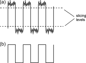 |
| Figure 11.12 Noise immunity of a digital signal. The noise affects the tips of the waveform, which can be squared by clipping (slicing) at suitable levels |
Figure 11.13 is a graph illustrating how these two types of signals behave when the signal-to-noise (S/N) ratio decreases by the same amount. The analog system is affected progressively, but the digital system is almost unaffected by the noise until a point is reached, when the system suddenly crashes as the bit error rate (BER) rises. This does not mean that digital methods cannot be used when the noise level is high, because there are a number of ways in which the information can be accurately recovered even from signals with a high BER. These methods are always used in digital recording systems [such as compact discs (CDs)] and for transmission systems (digital telephone links) and are the main reason for the widespread adoption of digital methods for signaling. A typical bit error rate for noisy conditions is 1 error in 1000 (a BER of 10
−3), and for better conditions, about 1 in 10,000 (BER
=
10
−4).
Note
Summary
Note
The effects of high BERs are very noticeable on digital television or radio broadcasting. Whereas a noisy analog signal provides a speckled picture of noisy sound, a digital signal with a high error rate can result in a still picture or a blank screen, and sound that is intermittent. The BER for television is usually high enough to avoid such problems, but DAB radio suffers considerably more because of poor transmitter coverage and inadequate antennae.
Summary
All forms of electronic signals are degenerated by noise. For analog signals, this is expressed as the signal-to-noise (S/N) ratio, and this figure should be high, typically 40
dB or more. For digital signals, the effect is expressed as bit error rate (BER), and this should be low, of the order of 1 in 1000 (10
−3) or 1 in 10,000 (10
−4) if data correction methods are to work well. The important difference between analog and digital methods is that whereas analog signals gradually deteriorate, digital signals are almost unaffected until the noise reaches a critical level, when the digital signal becomes totally garbled.
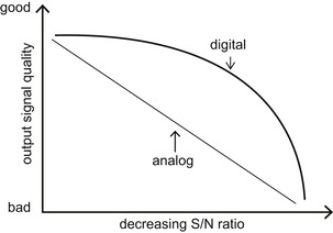 |
| Figure 11.13 Comparison of noise immunity for comparable analog and digital circuits |
The simplest type of system that can be used for correcting signals sent from a transmitter to a receiver is known as automatic request for repeat (ARQ). A standard code (American Standard Code for Information Interchange or ASCII) has for many years been used for teleprinters and computers. This uses two special code numbers that are referred to as ACK and NAK. If a distant receiver detects that a code pattern has no errors, it transmits back the ACK (Acknowledge) code. If errors have been detected, the NAK (Negative acknowledge) code is returned, and this is used to make the transmitter repeat the transmission of the last block of signal code.
A more advanced system is known as forward error control (FEC), and we have looked already at one version of this in Chapter 9, the use of parity bits. All FEC systems make use of the addition to the signal bits of extra redundant bits which, when suitably processed, are capable of identifying the errors and, in some cases, correcting the errors.
The main causes of bit errors in digital systems (and loss of signal in analog systems) are
white noise and
impulsive noise. White noise consists of a mixture of frequencies that is fairly evenly spread over the frequency range; no frequency is affected more than any other. This type of noise produces errors that are random. Impulsive noise, such as is produced by car-ignition systems, is at some definite pulse rate and it can create bursts of errors on each pulse. The errors that can occur are of three types, classed as detectable and correctable, detectable but not correctable, and undetectable (and therefore uncorrectable).
If an error can be detected but not corrected, it is possible that the error can be concealed in some way so that it causes less damage. For example, the system could ignore the error in a number and treat it as a zero level, or it could make use of the last known correct value again or it could calculate an average value based on the previous and next correct values. This last method is called
interpolation.
Using a Check Sum
The check sum is an error control scheme that is often used for digital recording systems, particularly magnetic disc and tape. The data must be organized into long ‘blocks’, each of which can be addressed by a reference number. For each block of digital data (numbers) the digital sum of the numbers, the
check sum, in a block is stored at the end of that block. When the data is recovered, the check sum can be recalculated from the block of replayed numbers and compared with the original to find whether any errors have occurred during reading or storage.
The simple check-sum technique can only identify when an error has occurred and cannot indicate whereabouts in the block the error is located. A modification of this method is called the
weighted check sum method, and it relies on the behavior of prime numbers (numbers that have no factors other than 1), such as 1, 3, 5, 7, 11, 13, etc. In a weighted check-sum system, each data number in a block is multiplied by a different prime number, and the check sum is calculated from this set of numbers. If a different check sum is found on replay, the difference between the calculated and the stored check sum is equal to a prime number, the same prime number as was used to multiply the data number that has been corrupted, so locating the number. The mathematical basis of this system is beyond the scope of this book but it is fascinating to see how an apparently academic study such as that of prime numbers can be put to a very practical engineering application. In mathematics and science, there is no such thing as useless knowledge, just knowledge that we do not yet need or know that we may need.
Summary
Summary
The use of ACK and NAK codes along with parity is a simple system for correcting transmitted data, but nowadays the use of systems such as check sums is more usual. The more advanced systems deal with a block of data numbers at a time, and can detect an error in the block, and correct this error if the coding allows its position to be located.
Hamming and Other Codes
Hamming codes are a form of error-correcting codes that were invented by R.W. Hamming, born in 1915, the pioneer of error-control methods. The details of Hamming codes are much too mathematical for this book, but the principles are to add check-bits to each binary number so that the number is expanded; for example, a 4-bit number might have three check-bits added to make the total number size seven bits. The check-bits are interleaved with the number bits, for example by using positions 1, 2, and 4 for check-bits, and positions 3, 5, 6, and 7 for the bits of the data number.
When an error has occurred, the parity checking of the check-bits will produce a number (called a
syndrome) whose value reveals the position of an error in the data. This error can then be corrected by inverting the bit at that position. A simple Hamming code will detect a single bit error, but by adding another overall parity bit, double errors can be detected. Hamming codes are particularly useful for dealing with random errors (caused by white noise).
The
cyclic redundancy check (CRC) method is particularly effective for dealing with burst errors caused by impulsive noise, and is extensively used for magnetic recording of data. Once again, the mathematical details are beyond the scope of this book, but in general, a data block is made up from three words, the data word, a generator code word, and a parity check code word. The data word is divided by the generator word to give the parity check word, and the whole block is recorded. On replay, the generator code is separated, and the whole block number is divided by this code. If the result is zero, there has been no error. If there is a remainder after this division, the error can be located by using this remainder along with the parity code.
The basic Hamming and CRC systems have been improved and developed over many years to produce digital systems that are more effective in dealing with both random errors and bursts of errors. These systems include BCH codes for random error control, Golay codes for random and burst error control, and Reed–Solomon codes for random and very long burst errors with an economy of parity bits. The Reed–Solomon coding system is used for CD recording and replay.
Summary
Summary
The more advanced methods of error detection and correction, ranging from simple Hamming codes through CRC to Reed–Solomon, all make use of added bits in a block of data and mathematical methods that allow the position of an error to be found. These methods also allow for error correction.
..................Content has been hidden....................
You can't read the all page of ebook, please click here login for view all page.