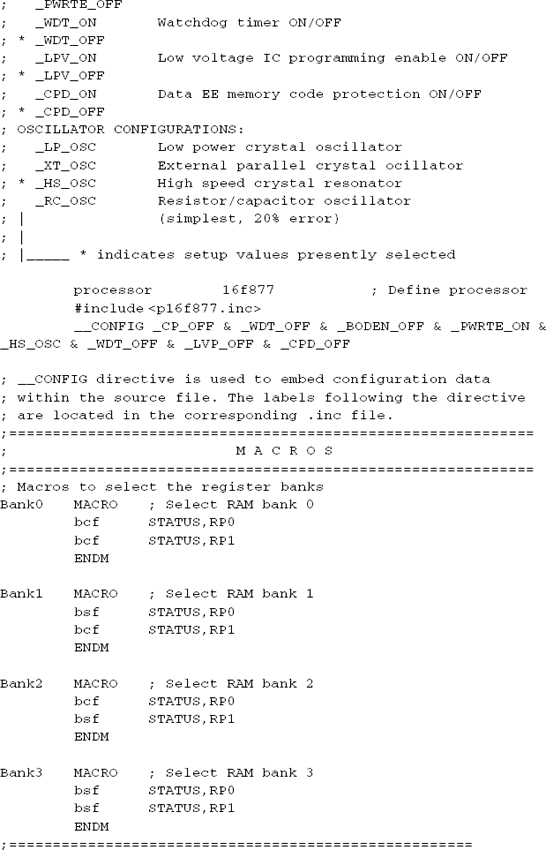
In this chapter we focus on digital communications techniques used in PIC interfacing with I/O devices, integrated circuits, and other forms of programmable logic. Communications, in general, refer to the exchange of information following rules, sometimes called a protocol. Digital and computer communications come in two flavors: serial and parallel. Serial communications take place when the data is sent one bit at a time over the communications channel. In parallel communications all the bits that compose a single symbol or character are sent simultaneously.
Popular lore regards serial communications as slower than parallel communications, but with modern-day technologies this is often not the case, as serial techniques often match or even excel parallel methods in speed and performance. Computer networks such as Ethernet and fiber-optic links are able to achieve high performance even though they use serial bit streams. The preference for serial over parallel communications is often more related to hardware, because parallel transmissions require more communication lines than serial transmissions.
20.1 PIC Communications Overview
Many communications standards were created with other interface and hardware requirements in mind and are not ideally suited for PIC applications. For example, RS-232-C, a serial protocol developed over 35 years ago, originated in an age of teletypewriters and modems. The voltage levels and circuit requirements of RS-232-C are not suited for PIC hardware. The more modern USB standard is more suited to PIC interfacing, but adopting a standard, RS-232-C, EIA-485, USB, or any other convention, requires adhering to special configurations in hardware and the use of ad hoc software protocols. This compliance with a standard comes at a price of added hardware components and increased software complexity.
When PIC-based circuits must interface with other systems or devices that follow these standards, then there is no alternative but to design circuits and write programs that comply with the standards. On the other hand, when the communications take place in dedicated circuits, which do not interface with devices or systems that follow standard communications protocols, then pure PIC communications techniques and hardware are often simpler and more effective. In other words, adhering to a communications protocol usually implies an additional cost in software and hardware complexity. Here are two examples: a PIC-based circuit that interfaces with a PC through the RS-232-C port would be a case where compliance with RS-232-C is required. Another case would be a PIC-based circuit that sends serial data to an onboard LCD display. In this case, the circuit and the software need not comply with any communications standards or protocols. Programmers often refer to techniques that use serial communications without the presence of specialized hardware, such as UART or USART chips, as bit-banging.
In the following sections, we discuss serial and parallel communications at their most essential level. In the general literature, communications concerns often focus on transmission speeds, system performance, and minimum processing time. Typically, PIC applications do not transfer large data files or communicate interactively on the Internet or in networks. In a typical PIC application, communication functions are used to upload stored data to a PC, sometimes called data-logging, or to receive small data sets or commands from a host machine. In this context there are no major concerns regarding super-fast transmission rates or maximum performance.
Serial communications take place by transmitting and receiving data in a stream of consecutive electrical pulses that represent data bits and control codes. The Electronic Industries Association (EIA) has sponsored the development of several standards for serial communications, such as RS-232-C, RS-422, RS-423, RS 449, EIA232E, and EIA232F, among others. In this designation the characters RS stand for the words Recommended Standard. The oldest, simplest to implement, and most-used serial communications standard is the RS-232-C voltage level convention. In the following sections we present the essential concepts of the RS-232-C standard. Most of the material also applies to the various updates of the standard. Later in the chapter we briefly discuss the EIA485 Standard.
20.2.1 Asynchronous Serial Transmission
The information in a serial bit stream is contained in a time-dependent waveform, that is, each bit code (data, control, or error) is transmitted for a fixed time period, known as the baud period. The word baud was chosen to honor the French scientist and inventor Jean Maurice Emile Baudot who studied various serial encodings in the late nineteenth century.
The serial bit streams used in data transmission follow a very simple encoding: one bit is transmitted during each baud period. A binary 1 bit is represented by a negative voltage level and a binary 0 bit by a positive voltage. The line condition during the logic 1 transmission is called a marking state, and the one for a logic 0 a spacing state. The baud rate is equal to the number of bits per second being transmitted or received. Note that the voltage levels that represent a 1 and a 0 bit in RS232 are somewhat counter-intuitive, as one would expect a logic 1 to be represented with a positive voltage, and not a negative one.
One possible approach to sending information bit-by-bit is based on the transmitter and receiver clocks being synchronized at the same frequency. That is, both receiver and transmitter operate at the same baud rate. Note that the expression “synchronized at the same frequency” implies not only that their clocks have the same speed, but that the high and the low portions of the waveform coincide.
In typical asynchronous serial communications, bits are transmitted as separate groups, usually seven to ten bits long. Each group is called a character. The name “character” relates to the fact that in alphanumeric transmissions each bit group represents one numeric or alphabetic symbol. In reality, the term “character” is also applied to control codes, error codes, and other nonalphanumeric encodings.
Each character is sent in a frame consisting of a start bit, followed by a set of character bits, followed (optionally) by a parity bit, and finalized by one or more stop bits. The serial line is normally held marking, that is, at a logic 1 state. The change from logic high to logic low, signaled by the start bit, tells the receiver that a frame follows. The receiver reads the number of character bits expected according to the adopted protocol until a logic high, represented by one or more stop bits, marks the end of the frame.
Figure 20-1 shows the different elements in a serial communications bit stream. The term asynchronous reflects the fact that the time period separating characters is variable. The transmitter holds the line to logic high (marking state) until it is ready to send. The start bit (spacing state) is used to signal the start of a new character. The start bit is also used by the receiver to synchronize with the transmitter. The logic high and low regions of the signal wave occur at the same time. This compensates for drifts and small errors in the baud rate.

Figure 20-1 Serial Communications Bit Stream.
This form of transmitting serial data is called asynchronous because the receiver resynchronizes itself to the transmitter using the start bit of each frame. The lack of synchronization does not refer to the bits within each frame, which must be in fact “synchronized,” but to the fact that characters need not come at a fixed time interval.
20.2.2 Synchronous Serial Transmission
An alternative approach to asynchronous serial data transmission is one in which the characters are sent in blocks with no framing bits surrounding them. In asynchronous communications, each character is framed by a start and a stop signal so that the receiver can know exactly where the character bits are located. In synchronous communications, the sender and receiver are synchronized with a clock or a signal that is part of the data stream.
In theory, synchronous communications implies that characters are sent out at a constant rate, in step with a clock signal. This scheme assumes that a separate line (or wire) is used for the clock signal, although, in some variations, the clock signal is contained in the transmitted characters. Alternatively, a clock line can be used to synchronize the moment in time at which the receiver reads the data line. In either case, it is this contained clock or command signal that identifies a synchronous transmission.
Most legacy PC communications systems are asynchronous, although the EIA232F standard supports both synchronous and asynchronous methods. The most common chip used in PC communications is the UART (Universal Asynchronous Receiver and Transmitter). An alternative chip called the USRT is used for synchronous communications and the USART (Universal Synchronous/Asynchronous Receiver and Transmitter) supports both.
Synchronous communications can be block or bit based. The block-based modes are also called character-based. In this mode, characters are grouped in blocks with each block having a starting flag, similar to the start bit used in asynchronous communications. Once the receiver and the transmitter are synchronized, the transmitter inserts two or more control characters known as synchronous idle characters, or SYNs. Then the block is sent and the receiver places the data in a memory storage area for later processing. Bit-oriented methods, on the other hand, are used for the transmission of binary data that is not tied to any particular character set.
20.2.3 PIC Serial Communications
Serial communications are often used in PIC programming, mostly due to the scarcity of available port lines. For example, an application in which a 16F84 PIC needs to read data in parallel from eight DIP switches and display the result, also in parallel, in eight LEDs, requires a total of 16 available port lines. But the 16F84 has only thirteen lines, eight in Port-B and five in Port-A; therefore, the application would not be feasible.
One possible solution is to find some way of reading the DIP switches serially; this requires three lines at most. Alternatively, the output data to the LEDs could be transmitted serially, thus reducing the total lines required from sixteen for parallel transmission, to six, or even less for serial transmission.
PIC communications can be designed both asynchronously and synchronously. Asynchronous modes are used when the same or compatible clock signals are available to both receiver and transmitter. For example, two PICs both running at the same clock rate can transmit and receive data using a single communications line, plus a common ground. PIC-to-PIC asynchronous data transmission mode is demonstrated later in this chapter with both circuit and code.
Asynchronous communications can be implemented by incorporating a dedicated IC, such as a UART or USART chip, in the circuit. PCs usually have one of these ICs, or functionally equivalent ones, in their implementation of the serial port. Some PICs include one or more serial circuits, which sometimes include a USART module. For example, the 16F877 PIC has two serial communication modules. One of them is the Master Asynchronous Serial Port, or MSSP. The other one is a USART. Later in this chapter we present serial communications programming examples using the USART module in the 16F877 PIC. Programs using the MSSP module are found in the chapter on EEPROM programming.
When communications take place between a PIC and a device that does not contain a clock, or whose clock runs at a different speed than the PIC’s, then synchronous communications is used. For example, a circuit can be designed using a shift register IC, such as the 74HC164, that performs an 8-bit serial-in, parallel-out function. In the previous example, it is possible to reduce the number of transmission lines by connecting the eight LEDs to the output ports of the 74HC164. But the 74HC164 contains no internal clock that runs at the speed of the 16F84. Thus, communications between the PIC and the shift register IC (74HC164 in this case) require a clock or command signal transmitted through a separate line; that is, a synchronous serial transmission. In this chapter we present circuits and sample code showing synchronous communications between a PIC and one or more shift register ICs.
RS-232-C was developed jointly by the Electronic Industries Association (EIA), the Bell Telephone System, and modem and computer manufacturers. The standard has achieved such widespread acceptance that its name is often used as a synonym for the serial port. EIA232F, published in 1997, is the latest update of RS-232-C. Today, RS-232-C is gradually being replaced by USB for local communications. USB is faster, has lower voltage levels, and uses smaller connectors that are easier to wire. USB has software support in most PC operating systems. On the other hand, USB is a more complex standard, requiring more complex software. Furthermore, serial ports are used to directly control hardware devices, such as relays and lamps, because the RS-232-C control lines can be easily manipulated by software. This is not feasible with USB.
In the following sections we describe the essential terminology and communications principles of RS-232-C.
The RS-232-C convention specifies that, with respect to ground, a voltage more negative than 3 V is interpreted as a 1 bit and a voltage more positive than +3 V as a 0 bit. Serial communications, according to RS-232-C, require that transmitter and receiver agree on a communications protocol. The following terminology refers to the RS-232-C communications protocol:
• Baud period: The rate of transmission measured in bits per second, also called the baud rate. In serial protocols, the transmitter and the receiver clocks must be synchronized to the same baud period.
• Marking state: The time period during which no data is transmitted. During the marking period, the transmitter holds the line at a steady high voltage, indicating logic 0.
• Spacing state: The time period during which data is transmitted. During the spacing period, the transmitter holds the line at a steady low voltage, indicating logic 1.
• Start bit: The transition that indicates that data transmission is about to start. The voltage low state that occurs during the start bit is called the spacing state.
• Character bits: The data stream composed of five, six, seven, or eight bits that encode the character transmitted. The least significant bit is the first one transmitted.
• Parity bit: An optional bit, transmitted following the character bits, used in checking for transmission errors. If even parity is chosen, the transmitter sets or clears the parity bit so as to make the sum of the character’s 1 bits and the parity bit an even number. In odd parity, the sum of 1 bits is an odd number. If parity is not correct, the receiver sets an error flag in a special register.
• Stop bits: One or more logic high bits inserted in the stream following the character bits or the parity bit, if there is one. The stop bit or bits ensure that the receiver has enough time to get ready for the next character.
• DTE (Data Terminal Equipment): The device at the far end of the connection. It is usually a computer or terminal. The DTE uses a male DB-25 connector, and utilizes twenty-two of the twenty-five available pins.
• DCE (Data Circuit-terminating Equipment): Refers to the modem or other terminal of the telephone line interface. DCE has a female DB-25 connector, and utilizes the same 22 pins as the DTE for signals and ground. DB-9 connectors are also used.
• Half-duplex: A system that allows serial communications in both directions, but only one direction at a time. Half-duplex communications are reminiscent of radio communications where one user says the word “Over” to indicate the end of transmission. In other words, half-duplex is similar to a one-lane road in which traffic controllers at each end can direct flow in either direction, but only in one direction at a time.
• Full-duplex: A full-duplex system allows communication in both directions simultaneously. A full-duplex system is reminiscent of a two-lane highway in which traffic can flow in both directions at once.
In the RS-232-C protocol, the transmission/reception parameters are selected from a range of standard values. The following are the most common ones:
Baud rate: 50, 110, 300, 600, 1200, 2400, 4800, 9600, and 19200
Data bits: 5, 6, 7, or 8
Parity bit: Odd, even, or no parity
Stop bits: 1, 1.5, or 2
RS-232-C defines DTE (Data Terminal Equipment) and DCE (Data Circuit-terminating Equipment), sometimes called Data Communications Equipment. According to the standard, the DTE designation includes both terminals and computers and DCE refers to modems, transducers, and other devices. The serial port in a computer is defined as a DTE device.
In RS-232 communications, a bit called a parity bit may optionally be transmitted along with the data. A parity bit provides a simple, but not too reliable, error test to detect data corruption that takes place during transmission. Parity can be even, odd, or none. Even or odd parity refers to the number of 1 bits in each data byte. The parity bit immediately follows the data bits.
If even parity is selected, the parity bit is transmitted with a value of 0 if the number of high bits is even. For example, the binary value
contains a total of four 1 bits; therefore, the parity bit is 0. By the same token, if even parity is selected, then the binary value
requires that the parity bit be 1. One way of describing the parity bit is to say that the bit is set to indicate a parity error; therefore, it serves as a parity error detector. Another description is that the parity coincides with the number of 1 bits in the data, plus the parity bit. Thus, when even parity is selected the parity bit is added to the number of 1 bits in the data to produce an even number.
Odd parity is the opposite of even parity. If odd parity were selected, then the parity bit in the previous example would be 0. Given odd or even parity, the sender counts the number of 1 bits and sets or clears the parity bit accordingly. The receiver, knowing that the parity is odd or even, can do likewise to determine if the number of 1 bits received matches the required parity setting.
Parity error checking is very primitive. In the first place, the parity error does not identify the bit or bits that cause the error. Furthermore, if an even number of bits are incorrect, then the parity bit would not show the error. On the other hand, over a long transmission, the parity check is likely to detect garbled data.
The RS-232-C standard requires specific hardware connectors with either twenty-five or nine pins. The twenty-five-pin connector is called a D-shell connector, or DB-25. The connector with nine pins is called the 9-pin D-shell connector or DB-9. In addition, the RJ-45 connector (the name stands for Registered-Jack 45) is used for twisted-pair cables. RJ-45 use in RS-232-C serial interface is regulated by the EIA/TIA-561 standard. A common application of RJ-45 connectors is in Ethernet cables. Figure 20-2 shows the male DB-25, DB-9, and the female RJ-45 connectors.
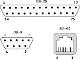
Figure 20-2 DB-25, DB-9, and RJ-45 Connectors.
The function assigned to each pin varies in the common connectors. Table 20.1 lists the assignation of the RS-232-C lines in the different hardware. The cable linking DTE and DCE devices is a parallel straight-through cable with no cross-over or self-connects.
Table 20.1
Definition of Common RS-232-C Lines
DB-25 |
CONNECTOR DB-9 |
RJ-45 |
FUNCTION |
CODE NAME |
DIRECTION |
1 |
4 |
Ground |
G |
||
2 |
3 |
6 |
Transmit data |
TXD |
Output |
3 |
2 |
5 |
Receive data |
RXD |
Input |
4 |
7 |
8 |
Request to send |
RTS |
Output |
5 |
8 |
7 |
Clear to send |
CTS |
Input |
6 |
6 |
Data set ready |
DSR |
Input |
|
7 |
5 |
Chassis ground |
G |
||
8 |
1 |
2 |
Carrier detect |
CD |
|
20 |
4 |
3 |
Data terminal ready |
DTR |
Out put |
22 |
9 |
1 |
Ring indicator |
RI |
Input |
The RS-232-C standards describe the way a computer communicates with a peripheral device, such as a modem. In this case, the DTE and DCE lines serve as a communications control. In this context, DTE means data terminal equipment, such as a computer, and DCE is the abbreviation for data communication equipment, such as modems. Often, communications must take place in an environment that does not include a modem; for example, computers communicating with each other or with other devices such as a PIC-based board. In these cases, the use of the DTE/DTE communication lines in flow control is not well defined. The common RS-232-C control and data signals appear in Table 20.2.
Table 20.2
Definition of Common RS-232-C Lines
SIGNAL NAME |
DIRECTION |
PURPOSE |
CONTROL SIGNALS |
||
Request to Send |
DTE -> DCE |
DTE wishes to send |
Clear to Send |
DTE <- DCE |
Response to Request to Send |
Data Set Ready |
DTE <- DCE |
DCE ready to operate |
Data Terminal Ready |
DTE -> DCE |
DTE ready to operate |
Ring Indicator |
DTE <- DCE |
DTE receiving telephone ringing signal |
Carrier Detect |
DTE <- DCE |
DTE receiving a carrier signal |
DATA SIGNALS |
||
Transmitted Data |
DTE -> DCE |
Data generated by DTE |
Received Data |
DTE <- DCE |
Data generated by DCE |
The term null modem refers to situations in which serial communications take place without the presence of a modem. In this case, the connection between the communicating devices, usually a cable, is wired in such a way so as to allow data transmission without a modem.
In Table 20.1, two pins are used in flow control: RTS (request to send) and CTS (clear to send). In conventional RS232 communication (as is the case when a computer communicates with a modem), the RTS signal is an output and DCE an input. Before a character is sent, the sender sets the RTS line high to asks the DTE’s permission. Until the DTE grants permission, no data is sent. The DTE grants its permission by setting the CTS line high. If the DCE cannot receive new data, it keeps the CTS signal low. This interface, which provides a simple mechanism for flow control in a single direction, is called a handshake.
In full-duplex transmission, the handshake must take place in both directions, that is, both devices must be able to signal their status. The DTR (data terminal ready) and DSR (data set ready) signals can be used for a second level of flow control. Finally, the CD (carrier detect) signal serves as an indication of the state of a modem.
Implementing handshaking without a modem requires that we take into account that two communicating devices can expect to find certain signals on given lines. For example, a device checks the CTS signal for a high value before sending data. If the CTS signal never goes high, transmission does not take place. When a cable is wired so that two devices can communicate without one of them being a modem, the cable is said to be a null modem.
One simple approach is to completely eliminate handshaking. In this case, cable wiring interconnects the transmit and the receive lines and the ground wire. The remaining pins are left unconnected, as shown in the null modem cable in Figure 20-3.

Figure 20-3 Null Modem with No Handshaking.
The three-wire null modem cable can be used to interface devices that do not use modem control signals. However, if one of the devices checks one of the handshake lines, such as RTS/CTS, then the three-wire modem cable fails. To solve this problem, a modem cable can be designed so that the handshake signals are interconnected; for example, DTS to DSR and vice versa. Not knowing which handshake signals are to be used, manufacturers of standard modem cables usually interconnect all handshake lines, as shown in Figure 20-4

Figure 20-4 Null Modem with Full Handshaking.
Some variations of the full-handshake null modem connect the DTR to the CD line at each end. Pin number 1 (CD) in both male and female connectors is dummied-out to pin number 4 (CDR).
A conventional, straight-through serial cable can be converted to null modem by means of a commercial null modem adapter that crosses over the corresponding signal lines. A continuity test is used to determine whether a serial cable is wired as null modem or not. If it is null modem, pin number 2 on one end would show continuity with number 3 pin on the other end.
A circuit tester is used to diagnose serial cables. The tester, which is plugged into the port connector, contains an LED for each of the communications lines. When the corresponding LED lights up, the line is active. LED colors indicate positive or negative voltages, with green usually indicating positive and red negative. The light pattern is used to identify different handshakes. Figure 20-5 shows a DB-25 mini tester.
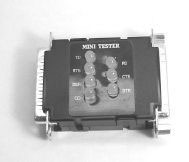
Figure 20-4 DB-25 RS232 Line Tester.
EIA-485 provides a two-wire, half-duplex serial connection standard, also known as RS-485. This convention provides a multipoint connection with differential signaling. The connection can be made full-duplex using four wires. In this standard, data is conveyed by voltage differences. One polarity represents logic 1 and the reverse one logic 0. The standard requires that the difference of potential be at least 0.2 volts, but any voltage between +12 and 7 volts allows correct operation.
EIA-485 does not specify a data transmission protocol, making possible the implementation of simple, inexpensive local network and communications links. Its data transmission speeds can reach 35 Mbits/s at distances of up to 10 m, and 100 Kbit/s at distances up to 1200 m. The use of a twisted wire pair and the differential balanced line allows spanning distances of up to 4000 m.
EIA-485 is often used with common UARTs and USARTs to implement low-speed data communications that require minimal hardware. It is also found in programmable logic controllers that are used with proprietary data communications systems. In factories and other electrically charged environments, the differential feature of EIA-485 makes it resistant to electromagnetic interference from motors and other equipment. The standard also finds use in large sound systems, such as those found in theaters and music events. EIA-485 does not specify any connector.
In PIC-based systems, EIA-485 is often used to provide strong serial signals that can travel up to 4000 m at high baud rates in noisy electrical environments. Only two wires are needed to carry the EIA-485 signals. These are usually labeled the A and B lines. Once the A/B data line is established, up to thirty-two devices can be connected to it. The system is referred to as an EIA-485 network.
Implementing the EIA-485 network requires some way of converting the 485 signal levels to the TTL-levels in the PIC circuit. This is accomplished by means of a dedicated IC, such as the Texas Instruments Differential Bus Transceiver chip called the SN75176. The chip actually converts 485 signals to RS-232-C TTL-level signals. This allows devices that traditionally communicate over RS-232-C serial connections to communicate over a two-wire EIA-485 network. Figure 20-6 shows the pin diagram of the SN75176.
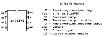
Figure 20-6 Pinout of the SN75176 IC.
In addition to the SN75176, an EIA-485 circuit requires a 485 chip such as the MAX485. In PIC-based systems, the EIA-485 is sometimes used to communicate with multiple devices in a chain. It uses the same 8-bit asynchronous serial communications format as was described previously for RS-232-C.
20.3 Parallel Data Transmission
Parallel communications is the process of sending several bits of data simultaneously over individual data lines. In the computer environment, parallel communications are often associated with a popular printer interface developed by Centronics and sometimes called the Centronics or printer interface. Originally, the Centronics interface was designed for one-way communications. Later, it was made bi-directional, allowing its use in high-speed data transfers. The Centronics or parallel printer interface is now considered a legacy port.
In PIC-based systems, parallel communications often refer to the general principle rather than to the specific Centronics implementation. For example, wiring an eight-line toggle switch to the eight pins of the 16F85 port-B line provides parallel communications between the switch and the PIC.
PIC circuits that use parallel data transfers offer many advantages. In the first place, parallel transmission is fast and the software is simple to develop. The hardware implementation is straightforward and does not require many additional components. Examples are connecting a multiple toggle switch to each of the lines of a PIC input port, or each of the pins of a Seven-Segment LED to the various pins of a PIC output port. The disadvantages of parallel systems are the distance limitations and the cost in system resources. Furthermore, parallel data transfers do not work well for data transmission over long distances. Many of the circuits and programs covered in previous chapters use parallel data transmission techniques. Because PIC-based systems rarely communicate with parallel printers or use the Centronics standard for data transfer, no further discussion of the Centronics standard is justifiable in this context.
20.3.1 PIC Parallel Slave Port (PSP)
Some PICs are equipped with an 8-bit Parallel Slave Port module (PSP). At present, the PSP is multiplexed onto Port D and is found in PICs of the mid-range family, such as the 16F877. The PSP is also called the microprocessor port.
The PSP module provides an interface mechanism with one or more microprocessors. The parallel slave port has an operating speed of 200 ns with a clock rate of 20 MHz, as well as several on-chip peripheral functions for implementing real-world in-terfaces. In PICs equipped with the PSP, the parallel slave port functions are assigned to port D, with some port E bits providing control signals. To initialize PSP mode, data direction bits in the TRISE register that correspond to RD, WR, and CS (TRISE<2:0>) are configured as inputs and the control bit PSPMODE (TRISE) is set. When the PSP mode is active, port D is asynchronously readable and writable through the chip Select (RE2/CS), Read (RE0/RD), and Write (RE1/WR) control inputs. At this time, not many general-purpose applications for the PSP port have been documented, outside of its use as a multi-microprocessor interface. For this reason we have excluded PSP programming from this context.
20.4 PIC “Free-Style” Serial Programming
This section is about PIC serial programming and circuit design that does not follow any specific communications protocol. In this sense, we have used the expression “free-style” as opposed to circuits and programs constrained by the requirements of a standard or convention. Many self-contained PIC circuits that do not interface with standardized components can benefit from not having to follow any specific standard. Later in this chapter, and in other chapters in the book, we present examples of PIC circuits and programs that follow established communications protocols. The titles of the corresponding sections refer to the specific standards or protocols; for example, the section titled “PIC RS-232-C Serial Programming” found in this chapter.
The advantages of so-called “free-style” circuit design and programming are greater ease in development and the use of fewer hardware components. When designer and programmer are not constrained by the specifications of a standard, the circuit can be implemented with a minimal number of hardware components. By the same token, software is simpler and easier to develop.
The following examples of free-style communications systems are presented in the sections that follow:
1. A PIC-to-PIC communications circuit and program. Two programs are required: one for the receiver PIC and one for the sender.
2. Serial-to-parallel and parallel-to-serial circuit and program. Circuit uses 74HC164 and 74HC165 ICs.
20.4.1 PIC-to-PIC Serial Communications
Perhaps the most obvious and straightforward mode of PIC serial communications is one that takes place between two PICs. In this case, one PIC acts as a sender, or master, and the other one as a receiver or slave, although it is also possible for sender and receiver to exchange roles. Consider a circuit in which one PIC polls the state of a bank of switches and then sends the result serially to a second PIC that controls a bank of LEDs to be lighted according to the switch settings. The reason for this circuit is that some PICs may not have a sufficient number of ports to monitor eight switches and control eight LEDs.
PIC-to-PIC Serial Communications Circuits
Actually, the system required for one PIC reading data and serially sending the result to another PIC that outputs the data can be visualized as two separate circuits. One circuit is used to read the state of the eight DIP switches and to send the data serially to another PIC circuit that displays the results. Figure 20-7 shows the two PIC-based circuits.
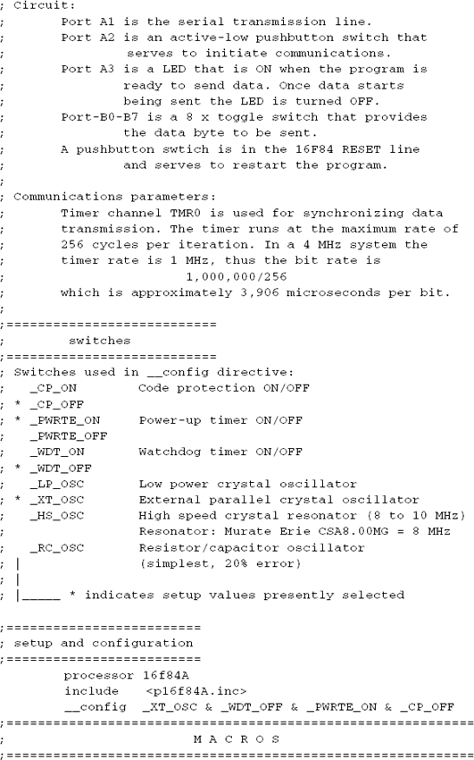
Structurally, the circuits in Figure 20-7 are quite similar to ones described previously in this book. The bottom circuit contains eight DIP switches wired to ports RB0 to RB7. A pushbutton switch is wired to port RA2 and an LED to port RA3. The serial output is through port RA1. The circuit at the top of Figure 20-7 has eight LEDs wired to ports RB0 to RB7. There is a pushbutton on port RA2 and an LED on port RA3. Input into the circuit is through port RA0. In the remainder of this description we refer to the bottom circuit as the sender circuit and PIC, and the one on the top as the receiver circuit and PIC.
The pushbuttons are necessary so that sender and receiver are synchronized. In operation, the receiver circuit is first activated by pressing the switch labeled “receive ready.” The LED on the top circuit lights to indicate the ready state. The sender circuit has an LED labeled “ready” that indicates its state. The user presses the switch labeled “send ready” in the sender circuit. At this time, the program in the sender reads the state of the DIP switches and sends the data out, one bit at a time, through the line labeled “serial out” in the diagram. The receiver reads the eight bits in its “serial in” line and lights the LEDs accordingly.
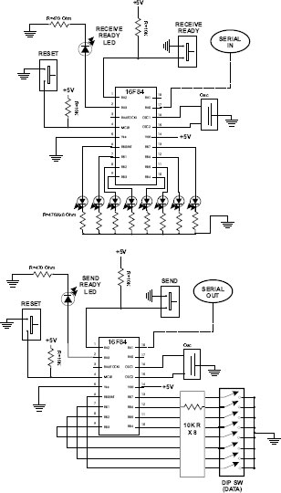
Figure 20-7 PIC-to-PIC Serial Communications Circuits.
PIC-to-PIC Serial Communications Programs
The software consists of two different programs, one to run in the sender PIC and one in the receiver PIC. Asynchronous communications require that sender and receiver operate at the same data speed. Both devices need not run at the same clock speed, but both must synchronize data transmission and reception at the same clock rate. Because the easiest way to accomplish this is to have both PICs use the same oscillator at the same speed, we make this assumption in the programs that follow.
The instruction time and clock rate of a PIC are one-fourth of its clock speed. Thus, a PIC with a 4-MHz clock runs at 1,000,000 cycles per second, and the default timer speed is
Approximately 3,906 us per clock cycle. Although 3,906 μs is not a standard baud rate, the present application is self-contained and there is no need to conform to RS-232-C or any other protocol.
Because it seems more intuitive to associate a high voltage with a logic 1 and a low voltage with a logic 0, we will adopt this convention in the current application. Nevertheless, we will borrow the character structure from the RS-232-C convention, that is, information will contain a start bit, a series of eight data bits, and a stop bit. No parity is implemented. Figure 20-8 shows the bit structure for one character in our application.
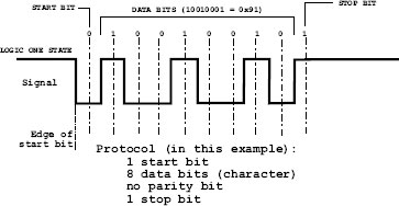
Figure 20-8 Data Structure for PIC-to-PIC Application.
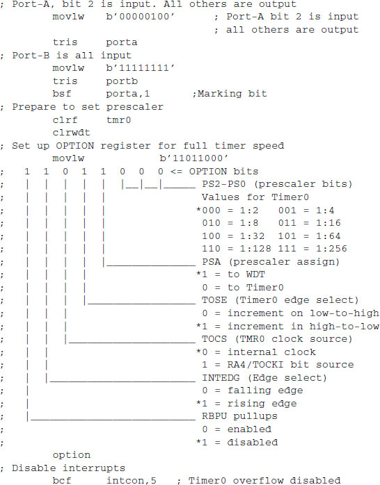
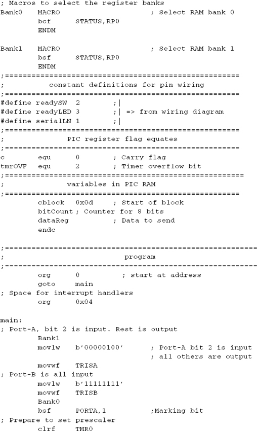
The sender program, named SerialSnd, performs the following initialization operations:
1. Line RA2 is initialized for input because the pushbutton switch is located on this line. Lines RB0 to RB7 are also input, as they are connected to the DIP switch array.
2. The prescaler is assigned to the Watchdog timer so that channel TMR0 runs at full processor speed.
3. Interrupts are disabled.
Initialization code is as follows:
Once initialized, the program performs the following functions:
1. The SEND READY LED is turned on.
2. Code monitors the SEND pushbutton switch.
3. Once the switch is pressed, the program turns off the SEND READY LED.
4. The state of the DIP switches is obtained by reading RB0 to RB7.
5. The byte from port B is sent through the serial line.
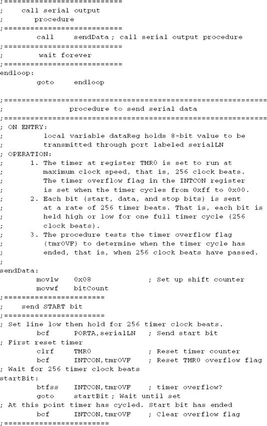
The following code fragment shows the procedure to send serial data:

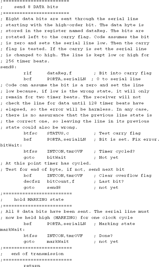
The code comments explain the routine’s operation.
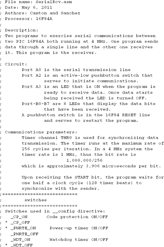
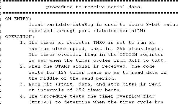
The receiving program, named SerialRcv, runs in the receiver PIC. In this case, the serial line is RA0. Input from the sender program is received through this line The program performs the following initialization operations:
1. Lines RA0 and RA2 are initialized for input because the pushbutton switch is lo cated on RA2 and RA0 is the serial input line. Lines RB0 to RB7 are output because they are wired to the eight LEDs.
2. The prescaler is assigned to the Watchdog timer so that channel TMR0 runs at full processor speed.
3. Interrupts are disabled.
Once initialized, code performs the following functions:
1. The SEND READY LED is turned on.
2. Code monitors the RECEIVE READY pushbutton switch.
3. Once the switch is pressed, the program turns on the RECEIVE READY LED.
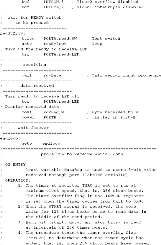
4. Code then monitors the serial line for the first low that indicates the leading edge of the start bit.
5. Once the start bit is detected, code waits for 128 clock cycles to locate the center of the start bit. This synchronizes the receiver with the sender and accommodates small timing errors.
6. The eight data bits are then received and stored.
7. After waiting for the stop bit, code turns off the RECEIVE READY LED and sets the eight LEDs according to the data received through the serial line.
The following code fragment is the procedure rcvData from the SerialRcv program:


Neither the SerialRcv nor the SerialSnd programs contain any handshake signal. The programs rely on the user turning on the receiver before the send function is activated. If this is not the case, the programs fail to communicate. But looking at the circuit diagram in Figure 20-7, we notice that there are available ports in both receiver and sender circuits. The circuit designer could interconnect two ports, one in the receiver and one in the sender, so as to provide a handshake signal.
For example, lines RA4 in both circuits can be interconnected. Then Port A, line 4, in the sender circuit is defined as input and the same line as output in the receiver. The receiver could then set the handshake line high to indicate that it is ready to receive. The sender monitors this same port and does not start the transmission of each character until it reads that the handshake line is high. In this manner, the receiver can suspend transmission at any time and prevent data from being lost. At the same time, the “receiver ready” and “send ready” LEDs can be eliminated.
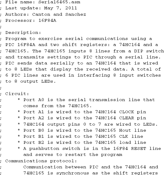
20.4.2 Program Using Shift Register ICs
The problem of handling multiple input and output lines, which was resolved in the previous example by using two PICs, can also be tackled by means of special-purpose integrated circuits. The term shift register refers to the fact that register input and output are connected in a way that data is shifted-down a set of flip-flops when the circuits are activated. Many variations of shift registers ICs are available, the most popular ones being serial-in to serial-out, parallel-in to parallel-out, serial-in to parallel-out, and parallel-in to serial-out. In shift register terminology, the in and out terms refer to the function in the registers themselves and are not related to the functions that these elements perform in a particular circuit. Figure 20-9 shows an input/output circuit using shift registers.
The circuit in Figure 20-9 shows the use of a parallel-to-serial IC (74HC165) that reads the state of eight input switches, and a serial-to-parallel IC (74HC164) that outputs data to eight LEDs. Without the shift register ICs, the circuit would require sixteen ports, more than those available in the 16F84. Using the shift registers, only six PIC ports are required, leaving eight ports available on the PIC. The demonstration program for the circuit in Figure 20-9 is called Serial6465.
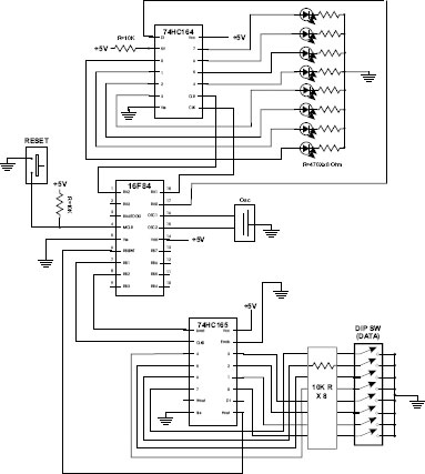
Figure 20-9 Input/output Circuit Using Shift Registers.
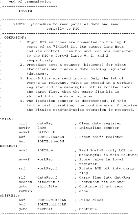
74HC165 Parallel-to-Serial Shift Register
The 74HC165 (sometimes called the 165) is a parallel-in, serial-out high-speed 8-bit shift register. Figure 20-10 shows the pin-out of the 74HC165.

Figure 20-10 74HC165 Pin-Out.
In the 165, pins 3 to 6 and 11 to 14 (labeled DO to D7) are used as parallel data input lines. Normally these pins are connected to input sources, such as switches or other two-state devices. Serial output takes place through pin number 9, labeled serial output Q. An inverted output is available at pin number 7. The shift/load control line, at pin number 1, is used to latch the data into the shift registers of the 165. For example, assume that the 165’s input lines are connected to sources that can change state in time. These highs and lows are not recorded internally in the 165 until the shift/load line is pulsed. When this line is pulsed, line values are said to be latched. After the data lines are latched, the 165 clock-line is pulsed in order to sequentially shift out each of the eight bits stored internally. Shifting takes place with the most-significant bit first. The actual operations are as follows:
1. A local data storage register is cleared and a local counter is initialized for eight data bits.
2. The 165 shift/load line is pulsed to reset the shift register.
3. The status of the serial output line (165 pin number 9) can now be read to determine the value of the bit shifted out.
4. The bit is stored in a data register and the bit counter is decremented. If the last bit was read, the routine ends.
5. If not, the clock line is pulsed to shift-out the next bit. Execution continues at Step 3.
The wiring of the 165 normally requires at least three interface lines with the PIC. One line connects to the 165 serial output (pin number 9), another one to the clock line (pin number 2), and a third one to the shift/load line (pin number 1). The eight data lines of the 165 are normally wired to the input source.
The following code fragment lists a procedure to interface a 16F84 PIC with a 74HC165 parallel-to-serial shift register:
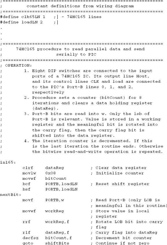
The procedure in165 is in the program Serial6465 listed at the end of this chapter.
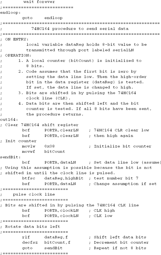
74HC164 Serial-to-Parallel Shift Register
The circuit in Figure 20-9 also uses a 74HC164 serial-to-parallel shift register for output to the eight LEDs. Figure 20-11 shows the pin-out of the 74HC164 IC.
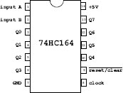
Figure 20-11 74HC164 Pinout.
Serial input into the 164 is through the input A line (pin number 1). Parallel output is through the lines labeled Q0 to Q7. The reset/clear line (on pin 9) and the clock line (on pin 8) provide the control functions. The operations are as follows:
1. A local data storage register holds the 8-bit value that serves as data input. A local counter is initialized for eight data bits.
2. The 164 shift register is cleared by pulsing the reset/clear line.
3. The first/next bit of the data operand is placed on the input line.
4. Bit is shifted in by pulsing the 164 clock line.
5. Bit counter is decremented. If it goes to zero, the routine ends.
6. Otherwise, the bits in the source operand are shifted and execution continues at Step 3.
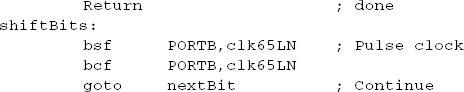
The following code fragment lists a procedure to interface a 16F84 PIC with a 74HC164 serial-to-parallel shift register:

![]()
It is important to note that serial communications that use shift register ICs are described as synchronous. Synchronous serial transmission requires that the sender and receiver use the same clock signal, or that the sender provide signal or pulse so as to indicate to the receiver when to read the next data element from the line. In the circuits discussed in this section, the shift/load, reset/clear, and clock lines provide this synchronous interface between the PIC and the shift register IC.
The program named Serial6465, in this book’s online software, is a demonstration of PIC-to-shift register interfacing.
20.5 PIC Protocol-Based Serial Programming
In the preceding sections we discussed circuits and developed software using PIC serial communications that did not conform to any particular protocol or standard. This style is adequate for stand-alone applications and circuits. On the other hand, PIC-based circuits sometimes communicate with systems that conform to a specific communications standard, for example, with a PC through its RS-232-C serial port. In this case, the PIC software and hardware must conform to the protocol, at least to an operational minimum that ensures satisfactory interfacing with the protocol-based system.
In the context of protocol-based programming, two situations are possible: either the PIC in use supports the communications standard or protocol, or it does not. In the case of the smaller PICs, such as the 16F84, the software emulates communications protocols because hardware provides no support. The more complex PICs, on the other hand, often contain hardware modules that provide a functionality equivalent to that required by the various standards. In this sense, mid-range and high-range PICs often include hardware support for one or more communication standards and conventions. For instance, the 16F87X PIC family includes an MSSP (Master Synchronous Serial Port) module and a USART (Universal Synchronous/asynchronous Receiver and Transmitter) module.
In the sections that follow we develop circuits and programs for cases in which the on-board PIC does not contain hardware support for the standard and for cases in which it does. Examples with PICs that do not provide hardware support for serial communications use the 16F84. Examples with PICs that provide hardware serial communications support use the 16F877, which contains an MSSP and a USART module. The 16F877 circuits and applications in this chapter use the processor’s USART module. The 16F877 MSSP module is demonstrated in the chapter on EEPROM programming.
20.5.1 RS-232-C Communications on the 16F84
The UART (Universal Asynchronous Receiver/Transmitter) controller is a serial communications IC found in computers and other data communication devices. In the PC, the UART was originally National Semiconductor INS8250. With the introduction of the PC AT, IBM changed its serial IC to the NC16450, an improved 8250. Later PCs adopted the NS16550A UART as their serial communications controllers. Other vendors, including Intel and Western Digital, furnish clones of the NS16550A and other UARTs.
The UART-based serial port implementation and circuitry in the PC is compliant with RS/EIA232. For a PIC-based circuit to communicate with a PC’s serial port, it must either implement in hardware or emulate in software the RS-232 signals and protocol. One possibility is to include a UART or UART-like IC in the circuit. But this option is not simple to implement because RS-232-C requires voltage levels that are not TTL-compatible.
For PIC-based systems without a UART module, a viable approach is to emulate UART functions in software, at least those required for interfacing with the PC hardware. This is quite feasible due to the availability of dedicated ICs that provide RS-232-C-compatible signals and voltage levels in systems in which a ±12 volt source is not available. These chips, sometimes called RS-232-C Drivers/Receivers or Transceivers, are especially useful in interfacing UART and USART-based systems with PIC-based hardware.
RS-232-C interface ICs are available from several vendors, although the ones from Dallas Semiconductors’ Maxim line are probably the most popular. These chips, sometimes called RS-232-C driver/receivers, have in common the use of so-called charge-pump DC/DC converters that generate, from the +5- volt TTL power source, the polarities and voltage levels required by RS-232-C.
One of the most popular implementations of the RS-232-C transceiver used in PIC-based systems is the MAX232 and its upgrade, the MAX202. One improvement in the MAX202 is to provide some degree of human-body electrostatic discharge protection (ESD), a desirable feature in experimenter boards. Other versions are the MAX233 and MAX203, which do not require external capacitors. Other RS-232-C transceiver ICs with various additional features, such as automatic shutdown, are available. Figure 20-12 is a pin-out of the MAX232 and MAX202 ICs.
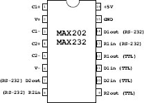
Figure 20-12 MAX202 and MAX232 Transceiver Pinout.
Note that the MAX232 and MAX202 consist of two drivers and two receivers per chip. Lines 14 and 7 (labeled D1out and D2out) provide RS-232-C output. Lines 13 and 8 (labeled R1in and R2in) are RS-232-C input. Lines 10 and 11 (labeled D1in and D2in) are TTL (or CMOS) inputs. Lines 9 and 12 (labeled R2out and R1out) are TTL output. In this designation the letter R stands for receiver and the letter D for driver. The digit 1 indicates the first driver/receiver set and the digit 2 the second one. The lines labeled D are wired to capacitors.
A circuit using the transceiver ICs is simple and easy to build. If a single communication line is required, then the TTL input line can be wired to pin 10 (D2in) and the TTL output to pin 9 (R2out). The RS-232-C input is wired to pin 8 (R2in) and the output to pin 7 (D2out). Later in this section we present a circuit that uses the MAX202 with a 16F84 PIC.
Often, a PIC-based circuit has to communicate with a device that conforms to a standard communications protocol. One of the most common cases is a PIC board that interfaces with a computer, usually a PC or Mac with an RS-232-C port. For example, a PIC board is placed somewhere to collect information, such as temperature, pressure, and humidity. Before the internal storage capacity of the PIC board is exhausted, it is connected to a laptop PC and the data is downloaded from the PIC board to the computer. Once this is done, then the local PIC memory is cleared so that new data can be collected and stored. This application, called a data logger, requires some way of transferring data from the PIC-based board to the PC. The RS-232-C line is often available on the PC end and the required interface hardware and programming are uncomplicated.
On the PC end, the communications software can be off-the-shelf applications or specially developed programs. If the purpose is simply to download data to the PC or send simple command to the PIC board, then a standard utility is used. For example, the Windows program named Hyper Terminal allows sending and receiving files and commands at various baud rates and RS-232-C communications parameters. Hyper Terminal is included with most Windows versions or can be downloaded free from the developer’s website.
The PIC board must have a system that conforms to the communications protocol of the device, in this case, the PC. In order to use the PC’s serial port, PIC hardware and software must be able to generate required signal levels, baud rate, and other RS-232-C communications parameters. Hardware interfacing is implemented using a transceiver chip, such as the MAX232 or 202 previously described. If the PIC contains a UART or USART module, then the communications software is easy to develop. This case is explored later in this chapter.
The terms teletype and teletypewriter refer to an obsolete electromechanical typewriter that was used to send and receive information through a simple communication channel. In a modern sense, TTY refers to a simple style of communications where the same device sends and receives text messages interactively. The current board is actually a TTY receiver because it does not contain a keyboard that allows sending data. Figure 20-13 shows the circuit diagram for a 16F84-based PC-to-PIC serial communications board.

Figure 20-13 PC-to-PIC Serial Communications Circuit.
The circuit in Figure 20-13 contains previously discussed components. The LCD is wired in 4-bit mode, with control lines for RS (reset), E (pulse), and R/W (read/write). The MAX202 provides the TTL-to-RS-232-C conversion and vice versa. The physical connection between the PC and the PIC board is by means of a DB-9 connector and a standard null modem cable. The cable is not shown in the circuit diagram.
The 16F84A PIC contains no built-in facilities for RS-232-C communications; therefore, a 16F84A application that communicates through the serial port using the RS-232-C protocol must emulate the protocol in software. The programs previously developed for PIC-to-PIC communications, discussed in Section 20.3.1, serve as a base for the UART emulation application. The major differences between a “freestyle” PIC communications program and one that complies with RS-232-C are the following:
1. Data must be transmitted and received at one of the standard RS-232-C baud rates. The most often-used baud rates in this case are 600, 1,200, 2,400, 4,800, 9,600, and 19,200.
2. Data must be formatted according to the protocol’s conventions; that is, a start bit, 5, 6, 7, or 8 data bits; the presence or absence of a parity bit; and 1, 1½, or 2 stop bits.
3. RS-232-C communication data is transmitted and received with the least-significant bit first.
The first problem (transmitting and receiving at a standard baud rate) often requires an approximation. The PIC’s instructions execute at the rate of its internal clock, which also determines the rate of its timer module.
The time taken by each counter iteration is obtained by dividing the PIC’s clock speed by four. For example, a PIC running on a 4-MHz oscillator clock increments the counter every 1 MHz. The counter register is incremented at a rate of 1 μs (assuming no prescaler). If we were to use the unmodified timer rate to measure bit time, the result would be a baud rate of approximately 3,906. Because 3,906 is not a standard baud rate, the timer is adjusted to approximate one of the standard
RS-232-C baud rates. For example, at 4,800 baud, the time per bit is
Because the timer of a PIC with a 4-MHz clock runs at 1 µs per timer iteration, we could count up from 0 to 208 iterations of the counter in order to approximate the bit time of 208 μs needed at 4,800 baud. In addition, we would have to calculate one-half the bit time because synchronization requires offsetting the timer from the edge to the center of the start bit (see Section 20.3.1). In this case, to delay approximately 104 µs we would count up from 0 to 104.
But counting up is inconvenient with the PIC timer/counter because the signal is produced when the counter reaches its maximum. A better solution is to preset the timer counter (TMR0) to a calculated value such that the desired time lapse occurs when the timer register reaches 255. So the actual delays for 4,800 baud are as follows:
Once we have obtained the clock rate for a standard baud rate, it is easy to obtain slower standard rates by slowing down the clock with the prescaler. For example, if the prescaler is assigned to the timer/counter register with a bit value of 000, then the counter rate is one-half the unscaled rate. This would produce a baud rate of 2,400 baud. By the same token, assigning a 1:4 prescaler to the timer produces a baud rate of 1,200 baud using the same preset values previously calculated. Faster baud rates are easily calculated by the same method.
Formatting the data transmission according to the RS-232-C protocol presents no major problem. In fact, the communications programs previously listed in this chapter use a start bit to commence character transmission, followed by eight data bits, and one stop bit to end it, with no parity bit. This same format is compatible with RS-232-C.
The third compatibility issue refers to the bit order in RS-232-C, which requires that the low-order bit be transmitted first. In previous applications, we have sent the high-order bit first by rotating the bits left inside the holding register and testing the carry flag. In the RS-232-C routine, the bits are rotated right into the carry flag and then the carry flag is rotated into the storage variable.
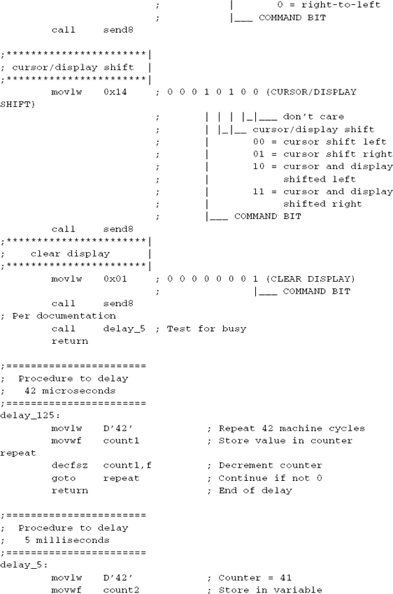
The demonstration program for the circuit in Figure 20-13, named TTYUsart, uses a two-line by sixteen-character LCD to display the characters received from the PC through the serial line. The program initially sends the test string “Ready-” to the PC to test the data transmission routine and to let the PC user know that the PIC board is ready to receive. The program operates at 2,400 baud, one start bit, eight data bits, no parity, and one stop bit. The communications program on the PC must be set to these parameters.
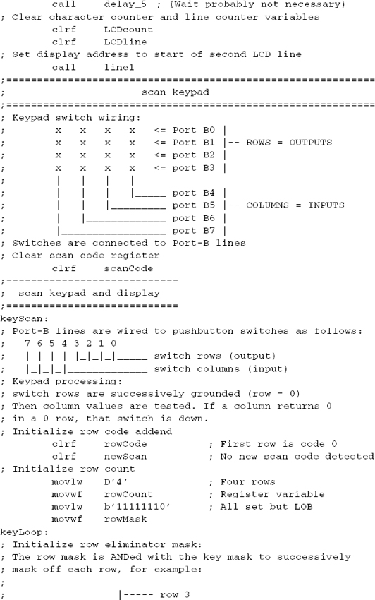
LCDs have limited capacity for data display. A two-line by sixteen-character LCD fills the screen when 32 characters are displayed. For some applications it is convenient to have a procedure that takes some reasonable action when the LCD screen is full. One approach is to detect when the last character in the second LCD line is displayed, then move the second line to the first line, clear the second line, and continue displaying at the start of the second line. This is the standard screen handling for a computer program.
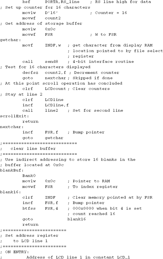
An LCD screen scroll routine can be called as each character is displayed. For the scroll to work, the program must keep track of the currently selected LCD line (variable LCDline can be 0 for line 1, and 1 for line 2), of the number of characters displayed on that line (variable LCDcount), and of the total capacity of the line (constant LCDlimit). Given this information, the logic for an LCD line scrolling routine can be as follows:
1. Add current character to LCDcount. If LCDcount is equal to LCD limit, then the end of a line was reached. If not, exit routine.
2. If line end reached is for line 1, set current display address to start of line 2. Reset variable LCDcount. Exit routine.
3. If line end reached is for line 2, then copy the characters displayed in line 2 to line 1. Clear line 2. Reset the display address to the start of line 2. Reset LCDline variable to line 2. Reset variable LCDcount. Exit routine.
Of these operations, copying the characters from the second line to the first one can be the most troublesome. One possibility is to read the data from the LCD directly. This approach requires that the connection between the PIC and the LCD include the R/W line. Another option is to create a buffer in RAM and copy each character displayed to this area. In the case of an LCD with sixteen characters per line, the buffer requires a capacity of 16 bytes. Because the line input is “remembered” in the buffer, the program scrolls a line by copying the contents of the buffer to the other line. This alternative does not require reading the LCD and saves implementing the R/W line.
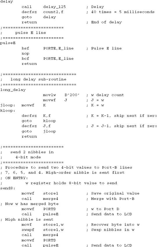
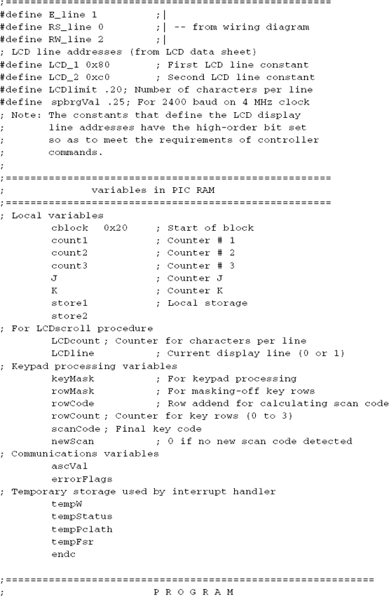
Storing the characters received in a local buffer first requires reserving a 16-byte area (the buffer) in PIC RAM. There are several ways of accomplishing this. A simple one is using the cblock directive, as shown in the following code fragment:

In reality, the buffer is most likely accessed by indirect addressing, so a buffer name (lineBuf in this case) is not really necessary. This is due to the fact that PIC assembly language does not contain a directive for finding the address of a variable. So the buffer address must be hard-coded or defined in a constant. But, in any case, having a buffer name does not cost storage capacity and it may help make the code clearer.
In our design, the scrolling routine depends on finding the characters in the ending line stored in the RAM area mentioned in the preceding paragraph. The buffer locations are accessed directly by referencing the address. For example, the first byte in lineBuf is stored at address 0x0c, the second one at 0xod, and so on. A more effective way of using a buffer is by creating and keeping a buffer pointer variable that has the current offset from the start of the buffer. The buffer pointer is then added to the buffer’s base address in order to access the current buffer location. Indirect addressing using the FSR and the INDF registers simplifies the process, as shown in the following code fragment:

The manipulation requires loading the base address of the buffer (0x0c in this case) in the w register, adding the value stored in the buffer pointer variable (bufPtr), and storing the sum in the FSR register. The character is then loaded into the w register and moved into the INDF register, which has the effect of storing it in the address pointer at by FSR. Conventionally, brackets are used to indicate indirect addressing, so [FSR] means the memory location referenced by the FSR register.
Once the line characters are stored locally, all that is left is the design of a line scrolling routine following the processing steps previously listed. The following procedure performs the necessary operations:


The entire program, named TTYUsart, is found in this book’s online software package.
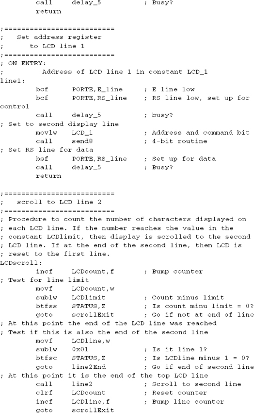
20.5.2 RS-232-C Communications on the 16F87x
The second alternative for protocol-compliant communications is using a PIC that provides hardware support for the standard. The 16F84, our workhorse in this book, contains no such facilities. However, other mid-range PICs do provide hardware support for one or several serial communications protocols.
For the examples that follow, we have selected what is perhaps the second most popular PIC of the mid-range family (after the 16F84): the 16F87x. The architecture and basic programming facilities of the 16F87x PIC family were discussed in Chapter 6. At this time, we should recall that 16F87x includes the PIC 16F873, 16F874, 16F876, and 16F877. For our sample programs we have selected the 16F877 because it is the most powerful one in the group. The 16F877 has an operating frequency of up to 20 MHz, 8K of flash program memory, 368 bytes of data memory, 256 bytes of EEPROM, five input/output ports, and two modules for serial communications: a Master Synchronous Serial Port and a Universal Synchronous/Asynchronous Receiver and Transmitter. We focus on the USART module and leave the MSSP for the chapter on EEPROM programming.
The Universal Synchronous Asynchronous Receiver Transmitter (USART) module in the 16F87X family is also known as a Serial Communications Interface, or SCI. The USART module is useful in communicating with devices and systems that support RS-232-C communications, including computers and terminals. It can be configured as an asynchronous full-duplex device, as a synchronous half-duplex master, or as a synchronous half-duplex slave. In the synchronous mode, the USART module is used mostly in communicating with analog-to-digital and digital-to-analog integrated circuits or for accessing serial EEPROM. Both of these functions were discussed in Chapter 14.
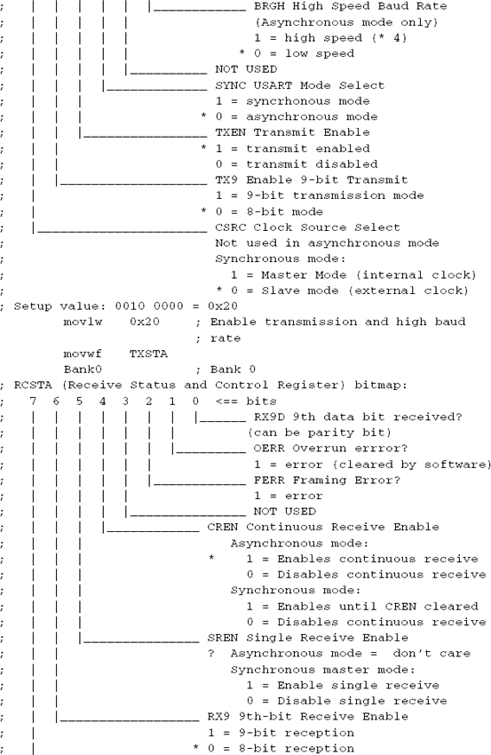
Five registers relate to USART operation in the 16F877: RCSTA, TXREG, RCREG, TXSTA, and SPBRG. The first three are located in bank 0 and the second two in bank 1. TXSTA is the Transmit Status and Control register and RCSTA is the Receive Status and Control register. Figure 20-14 shows the bitmap for the TXSTA register located at address 0x98 in bank 1.
The RCSTA register contains control and status bits for the receive function. The register is found at address 0x18 in bank 0. Figure 20-15 is a bitmap of the RCSTA register.
In the USART emulation programs for the 16F84, we were forced to approximate the RS-232-C baud rate with the system clock. The USART module in the 16F87X PICs contains its own baud rate generator, but it is also dependent on the system clock.
Setting the baud rate in the USART module consists of manipulating the Baud Rate Generator (BRG) unit. The BRG is a dedicated 8-bit generator that supports both the asynchronous and synchronous modes. The SPBRG is an 8-bit register that controls the rate of a dedicated timer. In the asynchronous mode, the bit labeled BRGH in the TXSTA register (see Figure 20-14) also relates to the baud rate because it allows setting either a slow-speed or a high-speed baud rate. The baud-rate-speed-select bit is inactive in the synchronous mode.
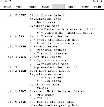
Figure 20-14 Bitmap of the TXSTA Register.
The formula for computing the baud rate takes into account the system oscillator speed (Fosc); the setting of the Baud-Rate-Speed-Select bit (BRGH), which is set for the high-speed mode and cleared for slow-speed, and also the setting of the SYNC bit in the TXSTA register, which selects either asynchronous or synchronous mode. The formula is as follows:
where ABR represents the Asynchronous Baud Rate, x is the value in the SPRGB register (range 0 to 255), S is 64 in the high-speed mode (BRGH bit is 1) and 16 in the slow speed mode (BRGH bit is 0). Solving the formula in terms of the value to be placed in the SPRGB register, we get
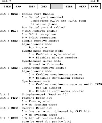
Figure 20-15 Bitmap of the RCSTA Register.
For example, to calculate the setting of the SPRGB register for 9,600 baud, with a 16-MHz oscillator, at the high-speed rate (S = 64) the equation becomes:
In this case, the value to store in the SPRGB register is 25. The actual baud rate can now be calculated using the first equation, as follows:
The percent error in the baud rate can be estimated by dividing the difference between the desired and the actual baud rate by the desired baud rate. The percent error is 0.16.
16F87x USART Asynchronous Transmitter
The USART in the 16F87x PICs uses a nonreturn-to-zero format, consisting of one start bit, eight or nine data bits, no parity, and one stop bit. In compliance with RS-232-C, the USART transmits and receives the least-significant bit first. Transmitter and receiver units are functionally independent but use the same data format and baud rate.
Although parity is not directly supported by the hardware, it can be implemented in software using the ninth data bit. Figure 20-16 shows the 16F87x registers related to asynchronous transmission.

Figure 20-16 16F87x Registers Used in Asynchronous Transmission.
The transmitter function also uses the Transmit Shift register (TSR), which is not mapped in memory and is thus not accessible to code. TSR obtains its data from the read/write transmit buffer, named TXREG, which is loaded in software after the stop bit is received. Then TXREG transfers the data to TSR and becomes empty. At this time the TXIF flag bit is set. An interrupt related to the TXIF bit is enabled/disabled by setting/clearing the TXIE enable bit in the PIE1 register. However, the TXIF flag bit is set regardless of the state of the TXIE enable bit. The TXIF flag is reset automatically when new data is loaded into TXREG.
While the TXIF flag indicates the status of TXREG, the TRMT bit, in TXSTA, reflects the status of TSR. TRMT is set when TSR is empty. This is a read-only bit. No interrupts are linked to the TRMT bit, so the program has to poll this bit to determine if TSR is empty. Transmission is enabled by setting the TXEN bit in TXSTA. The actual transmission does not occur until TXREG is loaded with data and the baud rate generator (BRG) has produced a clock beat. Alternatively, transmission can be started by loading TXREG and then setting the TXEN enable bit.
When transmission starts, the (not accessible) TSR register usually is empty. Thereafter, transferring data to TXREG results in a transfer to TSR, which then produces an empty TXREG. This mechanism makes possible the back-to-back transfer. Clearing the TXEN enable bit during transmission aborts the transmission. This action also resets the transmitter and sets the TX/CK pin high.
16F87x USART Asynchronous Receiver
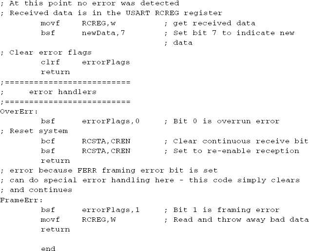
When Asynchronous mode is selected by setting the SYNC bit in TXSTA, then reception can be enabled by setting the CREN bit in the RCSTA register. Figure 20-17 shows the registers related to asynchronous reception.

Figure 20-17 Registers Used in Asynchronous Reception.
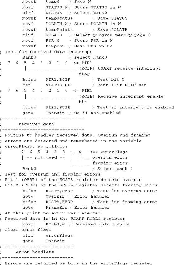
The main operational register is the RSR (Receive Shift Register), which, like TSR, is not accessible to application software. As soon as the stop bit is detected in the RX/TX pin, the received data in RSR is transferred to RCREG if it is empty. In this case, the RCIF flag bit is set. The interrupt linked to the RCIF flag is enabled or disabled by means of the RCIE in the PIE1 register. The RCIF flag bit is read-only and can be cleared only by hardware; this happens when the RCREG register has been read and is empty.
RCREG is double-buffered, meaning that it is possible for two bytes of data to be started simultaneously while a third byte begins shifting to RSR. If the stop bit is detected while RCREG is not empty, then the overrun error bit (OERR) is set in RCSTA. RCREG operates in first-in-first-out order. When it is read twice, the two bytes are retrieved in this order.
The overrun error bit (OERR) inhibits transfer from RSR into RCREG; therefore, it is important to clear this bit once the error is detected. The framing error bit (FERR) in the RCSTA register is set if a stop bit is not detected.
The following steps are followed in initializing and executing asynchronous reception:
1. The SPBRG register is set up for the selected baud rate.
2. Asynchronous reception is enabled by clearing the SYNC bit in the TXSTA register and setting the SPEN bit in the RCSTA register.
3. To enable the receive data interrupt, the RCIE, GIE, and PEIE bits must be set.
4. Reception is activated by setting the CREN bit in RCSTA.
5. When reception has concluded, the RCIF bit in the PIE1 register is set. At that time, an interrupt is generated if the RCIE bit was set.
6. Received data is retrieved by reading RCREG.
7. If any error occurred, the CREN bit must be cleared.
PIC-to-PC RS-232-C Communications Circuit
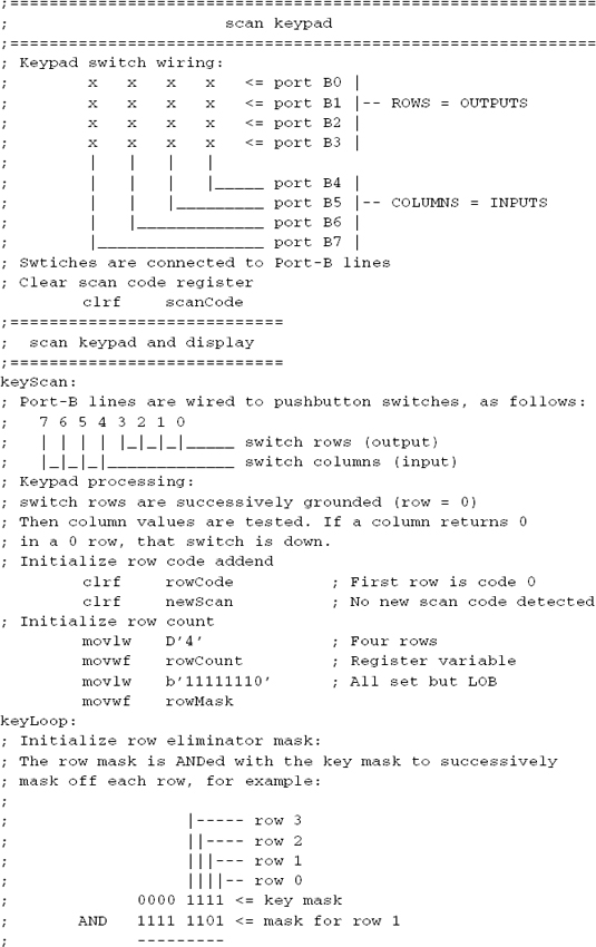
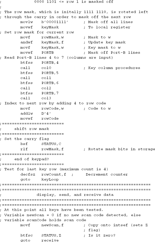
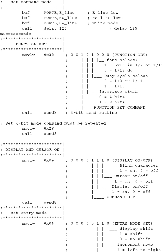
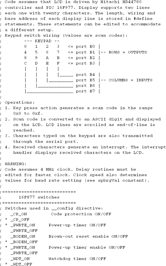
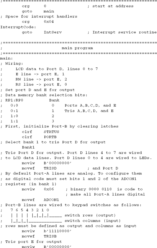
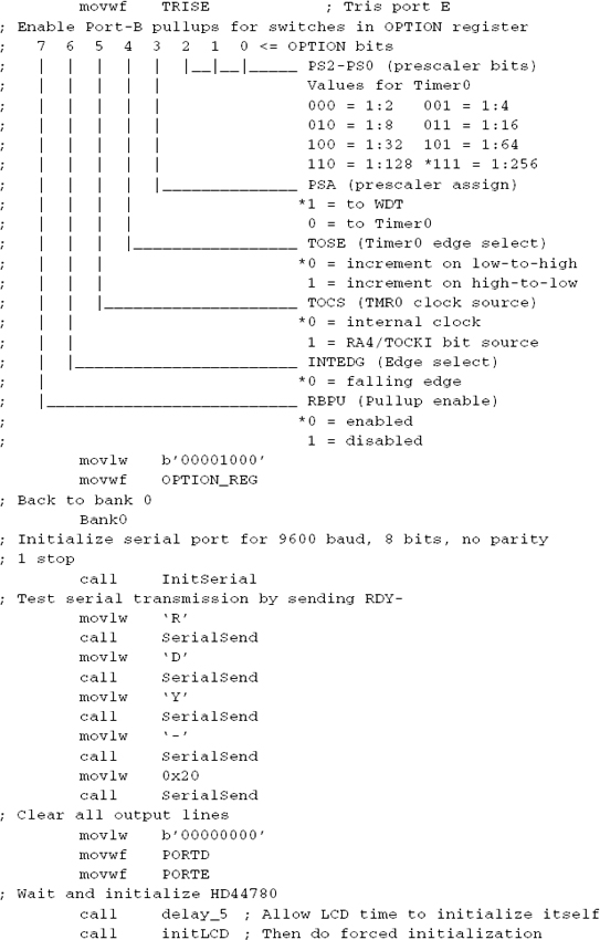
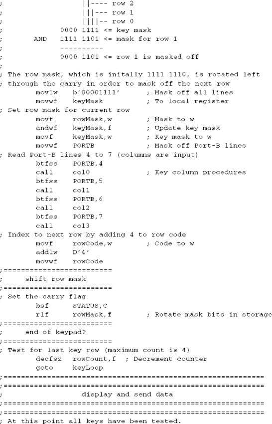
To demonstrate serial communications with the RS-232-C protocol we developed a circuit consisting of a 4-by-4 keypad and a 2-line by 20-character LCD display. Characters typed on the keypad are converted to ASCII codes for the hexadecimal digit set, that is, the numeral digits and the letters A through F. When a key is pressed, the corresponding ASCII code is displayed in the LCD and transmitted through the serial port to a PC application. Characters received though the serial line are displayed on the LCD. Figure 20-18 is a wiring diagram of the circuit.
The program SerComLCD demonstrates the circuit in Figure 20-18.
16F877 PIC Initialization Code
The following code fragment shows the initialization of the UART module in the 16F877 PIC for 2400 baud, 8 bits, no parity, and one stop bit. No interrupts are used in this example.


Figure 20-18 USART Communications Circuit with PIC 16F877.
USART Receive and Transmit Routines
The transmit data routine is quite simple. Code checks the TXIF bit in PIR1. If the bit is set, data is transmitted by storing the data byte in TXREG. The following procedure performs the required operations:
Receiving data is more complicated than transmitting it. One of the reasons is that code must test for and handle several possible errors that can occur during reception. The following code fragment shows the local variables and processing re-quired for simple data reception:

The procedures listed previously are from the program SerComLCD in the book’s online software. The applicable circuit is shown in Figure 20-18.
Polled routines for serial communications are adequate when the application does little else but check transmission lines. If the application has other tasks to perform, polled routines can waste processing time and even lose data. In this sense, the send function is usually less critical. An application can typically determine when to send data and have available all the data when the send operation activates. This is often not the case in receiving data, especially in applications that execute full-duplex.
A practical solution is to use interrupts for receiving characters through the serial line. The 60F87x includes facilities for implementing interrupt routines by both the send and the receive functions. To enable interrupts for the USART receive operation, the following preparatory steps are necessary:
• 1. Peripheral and global interrupts must be enabled by setting bits 6 and 7 of the INTCON register.
• 2. The receive interrupt must be enabled by setting the RCIF bit in the PIE1 register.
The handler for the serial reception interrupt usually performs the following functions:
1. The context is saved. This includes, but is not limited to, the status register, the w register, the PCLATH register, and the FSR register.
2. Code tests for received data by checking the RCIF bit in the PIR1 register. If this bit is clear, the interrupt did not originate in received data.
3. Code can also check if the interrupt enable bit (RCIE) is set in the RCIE register. If not enabled, the interrupt is related to serial data.
4. The handler usually checks two possible errors during reception: overflow and framing error. The first one by checking the OERR bit and the second one by checking the FERR bit, both in the RCSTA register. If reception errors have taken place, the handler takes appropriate action.
5. If no error is detected, then the received data can be retrieved from the RCREG.
6. On exit, the interrupt handler restores the context and issues the retfie instruction.
The following code fragment lists the variables and processing routine for an interrupt handler for serial data reception:


The program SerIntLCD in this book’s online software, is an Interrupt-Driven demonstration for the circuit in Figure 20-18.
The sample programs listed in the following sections refer to the programming discussed in this chapter.


![]()