
For students in courses in electrical, electronics, and computer engineering (or for anyone interested in these fields), hardware boards and programmers are a valuable learning tool. Many such boards are offered online at different prices and levels of complexity. But making your own demo boards is even more valuable than purchasing one off the shelf. In this appendix we provide information and resources to facilitate making hardware versions of three simple demo boards mentioned in the text.
The reader should note that these hardware boards are neither cheap nor easy to make. One of the problems is that companies that produce printed circuit boards often require orders for more than one board. For example, the company that we have often used in making printed circuit boards (ExpressPCB) provides a ProtoPro service of 4 boards per order. At the time of this writing the cost of a minimal order for each of the book’s demo boards was approximately $180.00. Which results in a cost of approximately $45.00 per board. Also in this appendix we provide information on producing home-made boards but this option has its own difficulties and drawbacks.
G.2 Printed Circuit Boards (PCBs)
PCBs are a nonconductive substrates (usually of fiberglass or resin) on which conductive traces and pathways are etched on one or more copper layers that are laminated onto board body. The result is an inexpensive and reliable media to which the electronic components can be attached, usually by welding.
Printed circuit boards are often created using a computer program that facilitates drawing the traces and placing the components onto one or more layers. Figure G-1 is a screen snapshot of the ExpressPCB program (furnished free on-line by ExpressPCB).

Figure G-1 PCB Being Developed with ExpressPCB.
A PCB editor program (such as ExpressPCB) generates a file from which the printed circuit board can be fabricated. Often the programs are proprietary of the firm that manufactures the boards. In the case of ExpressPCB, the file with the extension .pcb can be submitted online and the manufactured boards are returned to you in a few days.
In this book’s software package we include three files in .pcb format for the hardware version of each of the boards used in the text. The location and filenames are:
• PCBs/VBA/Demo Board A.pcb
• PCBs/VBB/Demo Board B.pcb
• PCBs/VBI/Demo Board I.pcb
These files can be used in having printed circuit boards made by ExpressPCB. In order to find out how to go about it you may log on to the company’s web site at www.expresspcb.com.
Once the printed circuits boards have been made, they must be populated with the electronic components. In order to facilitate this step, we are including a parts list for each of the boards in this book’s software package. The location and filenames are as follows:
• PCBs/VBA/parts demo a
• PCBs/VBB/parts demo b
• PCBs/VBI/parts demo c
The files are in .txt format and can be loaded and viewed in any word processing program or in Microsoft notepad.
In addition to the parts listed, the boards require a 9 to 12 volts AC/DC wall or table-top adapter. The power plug on the adapter should be female, 2.5 x 5.5 mm., and center positive polarity. Jameco part number 189238CJ is suitable. Similar ones are available at Radio Shack and from other sources.
G.4 Building Your Own Circuit Boards
Several methods have been developed for making printed circuit boards on a small scale, as would be convenient for the experimenter and prototype developer. If you look through the pages of any electronics supply catalog, you will find kits and components based on different technologies of various levels of complexity. The methods we describe in the following sections are perhaps the simplest because they do not require a photographic process.
The process consists of the following steps:
1. The circuit diagram is drawn on the PC using a general-purpose or specialized drawing program.
2. A printout is made of the circuit drawing on photographic paper.
3. The printout is transferred to a copper-clad circuit board blank by ironing over the paper’s backside with a household clothes iron.
4. The resulting board is placed in a ferric chloride etching bath that eats away all the copper, except the circuit image ironed onto the board surface.
5. The board is washed of the etching fluid, cleaned, drilled, and the components soldered to it in the conventional manner.
6. Optionally, another image can be ironed onto the front side of a double-sided board to provide a second conductive layer with or without components.
7. Images containing text, identification, or logos can be ironed onto either side of the board but are usually on the front side.
In this appendix we offer two examples: the first one consists of a simple demo board made on a single-sided board with text on the nonconductive side. The second one is the home-made version of Demo Board A that has two conductive sides and text on the front side.
The following tools and materials are required for fabricating the printed circuit board:
• A general-purpose drawing program or a specialized printed circuit drawing application.
• A laser printer such as LaserJet or equivalent or a laser copier. Inkjet printers are not suitable.
• Household clothes iron.
• Scotch - Brite™ (green) abrasive pads.
• Acetone solvent.
• Copper-plated circuit board blank, single- or double-side according to project.
• Ferric chloride etching solution for copper-plated boards.
• Plastic or glass container for holding board during etching.
After the board has been etched, it must be drilled and the components soldered. The following tools and materials are necessary for this phase:
• Small electric drill capable of high revolutions, such as a Dremmel tool.
• Drill bits 0.035" and 0.040".
• Soldering iron or soldering gun suitable for electronic components.
• Light duty rosin-core solder.
We have mentioned that hardware demonstration (or demo) boards are a useful tool in mastering embedded systems. Constructing your own demo boards and circuits is not a difficult task. The components can be placed on a breadboard, wire-wrapped onto a special circuit board. A printed circuit boards can be home-made, or one ordered through the Internet. The book’s online resource contains descriptions of commercial PCBs as well as instructions and resources for obtaining commercially made boards for the demo circuits used in this book.
We first illustrate the process with a simple board that contains a 16F84A-PIC, Seven-Segment LED, buzzer, pushbutton switch, and a bank of four toggle switches. Figure G-2 shows the schematics for the board and the power supply.
G.4.3 PCB Images for Demo Board
Commercial PCBs contain circuit etchings on two, four, or more layers. Although multi-layered boards appear complex, most circuit designers will agree that the more layers available the easier it is to place the components without interference. Double-sided boards (two conductive layers) usually have the power and interface connections on one layer and the ground plane on another one. That is the method we followed with the demo boards described in the online documentation and in this appendix. In this case, two circuit board images are required, one for each conductive plane on the board. In addition, most boards contain a text image that includes component placements, company logos, model numbers, and other textual information. In commercially made boards, the text image is silk-screened onto the board.
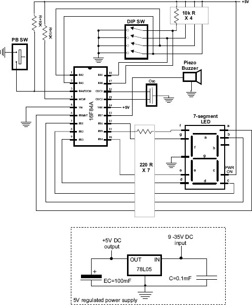
Figure G-2 A Simple PIC 16F87A Demo Board.
The first home-made board example in this appendix uses a single-sided board with an etched image on the conductive side (bronze layer) and a text image on the board’s nonconductive side. Both images can be created with a conventional drawing program, such as Corel Draw, Adobe Illustrator, or Windows Paint, or with a specialized application, such as the one furnished by ExpressPCB and discussed earlier in this appendix. Figure G-3 shows the images used for making the PCB for the circuit in Figure G-2.

Figure G-3 Bottom-Side and Top-Side Layer Images for a PCB.
In Figure G-3 the image on the left side is etched on the conductive side of the board, that is, the one with the copper layer. This is usually referred to as the bottom layer. In this example the components and the text are placed on the top or nonconductive layer. Notice that the top-side image must be horizontally mirrored before it is transferred to the photographic paper. This is necessary so that the text and graphics coincide with the circuit etchings.
Any computer drawing program serves this purpose. We have used CorelDraw™, but there are several specialized PCB drawing programs available on the Internet. Notice in the drawing in Figure G-3 that the circuit locations where the components are to be soldered consist of small circular pads, usually called solder pads. Figure G-4 zooms into a PCB drawing to show the details of the solder pads.
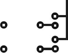
Figure G-4 Detail of Circuit Board Pads.
Quite often it is necessary for a circuit line to cross between two solder pads. In this case the pads can be made smaller or modified so as to allow passing a trace between them. Modified pads are shown in Figure G-5.
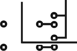
Figure G-5 Modified Circuit Boards Pads.
In the method presently described the circuit diagram is printed using a laser printer. Inkjet toners do not produce an image that resist the action of the etching liquid. Although in our experiments we used LaserJet printers, it is well documented that virtually any laser printer will work. Laser copiers have also been used successfully for creating the PCB circuit image.
However, with this method the width of the traces can become an issue. The traces in the PCB image of Figure G-5 are 2 points, which is 0.027". Traces half that width and less have been used successfully; but as the traces become thinner the entire process turns out more critical. For most simple circuits, 0.020" traces should be a useful limit. Be careful not to touch the glossy side of the photographic paper or the printed image with your fingers.
Practitioners of this method affirm that one of the most critical elements is the paper used in printing the circuit. Pinholes in some papers can degrade the image to the point that the circuit lines (especially if they are very thin) do not etch correctly. Another problem relates to removing the ironed-on paper from the board without damaging the board surface.
Glossy, coated inkjet-printer paper works well (yes, Inkjet paper on a LaserJet printer). Even better results can be obtained with glossy photo paper. We use a common high-gloss photographic paper available from Staples and sold under the name of “picture paper.” The 30 sheets, 8-by-10 size, has the Staples number B031420197 1713. The UPC barcode is: 7 18103 02238 5.
Transferring the image onto the board blank is done by applying heat from a common clothes iron, set on the hottest setting, onto the paper/board sandwich. In most irons the hottest setting is labeled “linen.” After going over the back of the paper several times with the hot iron, the paper becomes fused to the copper side of the blank board. The board/paper sandwich is then allowed to soak in water for about ten minutes, after which the paper can be removed by peeling or light scrubbing with a toothbrush. It has been mentioned that Hewlett-Packard toner cartridges with so-called microfine particles work better than store-brand toner cartridges.
Once the paper has been removed and the board washed, it is time to prepare the board for etching. The preliminary operations consist of rubbing the copper surface of the board with a Scotchbrite abrasive pad and then scrubbing the surface with a paper towel soaked with acetone solvent.
Once the board is rubbed and clean, you can proceed to etch the circuit. The etching solution contains ferric chloride and is available from Radio Shack as a solution and from Jameco Electronics as a powder to be mixed by the user. PCB ferric chloride etchant should be handled with rubber gloves and rubber apron because it stains the skin and utensils. Also, concentrated acid fumes from ferric chloride solution are toxic and can cause severe burns. These chemicals should be handled according to cautions and warnings posted on the containers.
The ferric chloride solution should be used in a plastic or glass container, never in metal. Faster etching is accomplished if the etching solution is first warmed by placing the bottle in a tub of hot water. Once the board is in the solution, face up, the container is rocked back and forward. It is also possible to aid copper removal by rubbing the surface with a rubber-gloved finger.
The etched board should be washed well, first in water and then in lacquer thinner or acetone, either solvent works. It is better to just rub the board surface with a paper towel soaked in the solvent. Keep in mind that most solvents are flammable and explosive, and also toxic.
After the board is clean, the mounting holes can be drilled using the solder pads as a guide. A small electric drill at high revolutions, such as a Dremmel tool, works well for this operation. The standard drill size for the mounting holes is 0.035". A #60 drill (0.040") also works. Online one can purchase a set of special PCB drill bits of various sizes. Once all the holes are drilled, the components can be mounted from the front side and soldered at the pads.
The component side (front side) of the PCB can be printed with an image of the elements to be mounted or with logos or other text. A single-sided blank board has no copper coating on the front side, so the image is just ironed on without etching. Probably the best time to print the text image is after the board has been etched and drilled but before mounting the components. Double-sided boards must be etched and washed before the text image is transferred.
Assembling and soldering components onto PCBs require some manual and technical skills, materials, and special equipment. We do not recommend that you undertake this task unless you have previous experience in this area. Neither do we provide information or assistance on how to do it.
The parts listed were available at the mentioned sources and the listed prices at the time of writing. Availability and prices often change, so it may not be the case when you place your order.
The sources recommended for the PVBs and the electronic components are ones that we have used in the past and are popular with experimenters and hobbyists. But there are many other sources that can supply equivalent parts at the same or perhaps better prices. The authors and publishers of this book have no association with or commercial interest in any of the sources mentioned.