
4
Spatial and Spectral Resolution of Semiconductor Detectors in Medical Imaging
Bjorn Heismann
CONTENTS
4.2.1 Indirect and Direct Conversion Detectors
4.2.2 Signal Transport Processes
4.3.1 Definition of the Modulation Transfer Function
4.3.2 Simulation and Measurement of the MTF
4.4.1 Definition of the Detector Response Function
4.4.2 Comparison of the Detector Response Functions
4.4.3 Integrating Indirect Conversion Detectors
4.1 Introduction
Medical imaging devices commonly use gamma and x-ray radiation to generate internal images of the human body. Single photon emission tomography (SPECT) and positron emission tomography (PET) systems detect gamma emissions of radionuclide tracers. Computed tomography (CT), radiography, and mammography systems measure the x-ray attenuation of the human body. Figure 4.1 outlines the modes of operation of SPECT, CT, and radiography devices.
The image quality and dose usage of these systems are strongly influenced by the employed radiation detectors. From the early stages on, scintillator detectors based on materials like NaI, BGO, LSO, GOS, and CsI performed the first step of radiation detection [1]. Over the past few years, an increasing number of scientific and commercial activities have used conversion semiconductor detectors for medical imaging. For lower x-ray energies, amorphous selenium detectors are routinely employed in mammography detectors. For higher x- and gamma ray energies, CdZnTe and CdTe have come into focus. SPECT prototypes in cardiology, scintimammography, and small animal imaging have been presented; see, for example, [2–4]. The authors report the improved spectral resolution and underline the potential to perform dual-isotope imaging. For CT, direct conversion counting electronics and prototype systems have been built and evaluated [5–8]. The high x-ray flux of more than 108 quanta per s and mm2 is found to be a major challenge. A main reason for this is attributed to the dynamic material properties of CZT. It has been shown that defects like Te inclusions and subsequent inferior hole mobility lead to polarization in CZT detectors under medical imaging x-ray fluxes [9–12]. The main mechanism is seen in the creation of a dynamic space charge in the semiconductor bulk, degrading the charge transport properties. The potential benefits of semiconductor detectors in medical imaging rely mainly on their spatial and spectral resolution. In this chapter, we ana-lyze the signal transport in both a scintillator and a semiconductor detector. As an application example, we focus on a CT detector. The pixel geometry, scintillator material, and thickness as well as the electronic read-out are chosen accordingly. As figures of merit, we use the modulation transfer function to quantify the spatial resolution and the detector response function D(E,E0) to analyze the spectral behavior. It should be noted that the results indicate an upper performance limit since degradations by, for example, material defects are not included.

FIGURE 4.1
SPECT, CT, and radiography medical imaging devices.
4.2 Detector Physics
4.2.1 Indirect and Direct Conversion Detectors
The indirect conversion scintillation detector in Figure 4.2 is based on a GOS scintillator bulk material. Each pixel is enclosed by an epoxy compound filled with back-scattering TiO2 particles. Typical pixel dimensions of around 1 mm and below are obtained. A registered photo sensor detects the secondary light photons at the bottom surface of each pixel. The primary interaction in a detector pixel is given by absorption of an incoming x-ray quantum by a gadolinium atom. The x-ray energy is converted into light photons. The energy conversion rate is around 12% [13]. Secondary light photon transport takes place. Photons which reach the photosensor contribute to the output energy signal E0. Radiography and mammography detectors follow similar designs. CsI is usually employed as a scintillator. Due to its vertical needle structure, it has the advantage of providing intrinsic light guiding properties, thus no back-scattering septa are required. This allows for an improved detector resolution at the expense of a reduced stopping power and signal speed.
Two main physical effects influence the spatial and spectral resolution in pixelized scintillator detectors. First, the primary energy deposition is not perfectly localized. For the high-Z atom gadolinium, absorption is governed by the photoelectric effect. This generates fluorescence escape photons with mean free path lengths in the order of several 100 μm. They might be reabsorbed in the pixel volume, become registered in a neighboring pixel, or leave the detector volume completely. Second, light transport is affected by optical cross-talk. Septa walls are designed with a limited thickness to optimize overall dose usage and light yield. As a consequence, a significant portion of the light is transferred to adjacent “false” pixels, see Figure 4.2.
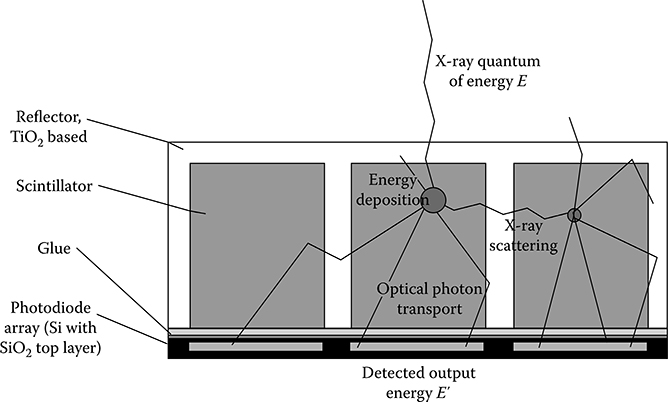
FIGURE 4.2
Schematics of a CT scintillation detector as an example for an indirect conversion detector.

FIGURE 4.3
Schematics of a common cathode CZT direct conversion detector.
The direct conversion CZT scheme is shown in Figure 4.3. A common-cathode design with pixelized anodes on the bottom surface of the semiconductor bulk is typically used. Pixels are established by funnel-shaped electrical fields of several 100 V/mm. The physics of the primary energy deposition are comparable to the indirect conversion detector. However, the deposited energy is converted to charges instead of optical photons. The holes and electrons are separated and accelerated by the electrical field. Electrical pulse signals are induced on the electrodes. The main signal pulse is generated when the electrons follow the stronger curved electrical field in the bulk region close to the anodes.
The main signal degradation mechanisms are comparable to indirect conversion scintillator detectors. First, fluorescence scattering takes place. Due to the lower K-edge energy, the mean free path lengths of fluorescence quanta in CZT are about 100 μm. The smaller the pixel size, the more fluorescence cross-talk will affect the behavior of the detector. Second, the charge signal transport is affected by charge sharing. The moving charge cloud also induces electrical pulses on neighboring pixels [14], again mostly at the bottom part of the pixel field configuration.
Figure 4.4a through e summarizes the main difference between an indirect conversion scintillator detector and a direct conversion semiconductor detector. The scintillation detector is an optical device using light photons as intermittent information carriers. A direct conversion detector omits the conversion to light and directly generates charge carriers. It is an electrical device which employs electrons and holes to transfer the event information to the electrodes.

FIGURE 4.4
Signal conversion steps in an indirect conversion detector (a–c) and a direct conversion detector (d–e).
Both detector types can be operated in an integrating or a counting mode. In integrating mode, the charge information is sampled over an integration time—and converted to a digital signal. In counting mode, the total number of events is measured by counting the charge pulses. In addition to this, the energy of each absorbed quantum can be obtained by measuring the total charge or pulse amplitude of each quantum. Counting detectors thus offer spectral resolution of the input quantum field.
TABLE 4.1
Detector Simulation Parameters Material

Note: We neglect electronic noise in the indirect conversion detector. It does not influence the spatial and spectral resolution comparison significantly. A threshold noise level of 3 keV (root mean square) is assumed for the direct conversion approach.
The detector parameters for our comparison are summarized in Table 4.1. For the scintillator detector, a 1.4 mm thick GOS with a pixel size of 1.2 mm has been chosen. The direct conversion detector has a 2 mm thick CZT at 700 V bias with a quadratic pixel size of (450 μm)2. For this pixel size, fluorescence cross-talk contributes significantly. The choice reflects mostly the high-resolution case. The spatial resolution is not directly comparable to the scintillator detector. The setting is chosen to investigate if a direct conversion detector can provide improved spatial resolution at a reasonable spectral resolution.
4.2.2 Signal Transport Processes
Figure 4.5a and b outlines the cascaded system theory (CST) model of an indirect conversion integrating and a direct conversion counting detector. CST models have been applied to a number of detector evaluations, especially for flat panel radiography and mammography detectors [15].
The indirect conversion detector in Figure 4.4a has the following signal conversion steps. First, the X or gamma quantum is absorbed and its energy is converted to light photons. Second, the light photons travel through the scintillator set-up. Third, light photons are detected as an electrical current by the photo sensor. Finally, the current signal is digitized by a sampling ADC. The first step of the direct conversion detector in Figure 4.4b also consists of the x-ray energy deposition. A cloud of electrons and holes is generated. Second, the generated charges travel to the electrodes, forming current pulses. Finally, the current pulses are detected by a read-out electronic.
The signal transport can be simulated by a cascade of independent conversion steps. For the indirect conversion detector this can be done as follows [13]:
Primary energy deposition
The primary energy deposition is modeled by a Monte Carlo simulation tool based on the GEANT4 particle interaction simulation framework [16–18]. For each incoming x-ray quantum, the spatial energy deposit is simulated on a 10 × 10 × 10 sub-voxel grid. Rayleigh and Compton scattering and escape processes generally lead to multiple deposition sites per event. Each portion of the primary energy deposit is converted into a number of optical photons, taking into account the main scintillator photon emission energies. The energy to optical photons conversion gain for Gd2O2S:Pr is taken from measurements as Ec = 0.12 with a standard deviation of σ(Ec) = 0.04. As a result of the first step, we obtain a look-up table of individual energy deposition events. By using a high number of events (106 and more), systematic errors are avoided.
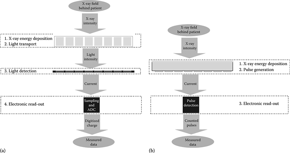
FIGURE 4.5
Cascaded detection models: (a) indirect conversion, (b) direct conversion.Light transport
The second step describes the light transport to the photo sensor pixels. A photon tracking Monte Carlo simulation [13] traces the photon paths in the entire detector system until they are detected at a pixel of the photo sensor array or lost by bulk absorption or scintillator escape. Photon interaction processes like optical scattering, photon reabsorption and diffuse and specular reflection at pixel septa borders are included. The corresponding optical parameters are taken from experimental results. For a specific photon starting position, the average detection probability of an optical photon in a photo sensor pixel is obtained.
Light detection
The light photons that have reached a photo sensor pixel are converted to electrical charges. The wavelength-dependent quantum efficiency β(λ) of the photo sensor is taken into account. As a result of the third step, we obtain a photo current for each pixel.
Electronic read-out
In the final step, the photo current is sampled to charge and digitized. For medical x-ray applications, sigma-delta ADCs are common ADC designs. Direct current measurements by a charge-coupled oscillator are also employed. The electronic read-out usually has limited linearity and additional offset noise. For the results in this chapter, non-linearity and electronic noise do not play a role and are neglected.
For a given detector geometry, x-ray quantum input spectrum and field distribution, this scheme yields the average signal of the scintillator detector. The signal chain of the direct conversion detector in Figure 4.4b is modeled as follows [19]:
Primary energy deposition
The primary energy deposition step is equivalent to the scintillator model. Instead of a GOS material, a CZT absorber is used.
Pulse generation
A detailed charge transport model can be based on the work of Eskin et al. [20]. A local weighting potential allows to calculate the signal pulse shape for arbitrary charge starting positions in the detector [21]. A time-resolved pulse signal on the anode is obtained.
Electronic read-out
Depending on the priority of spectral or spatial resolution, two main electronic design schemes for direct conversion detectors can be selected. Spectrally resolving detectors in SPECT and PET require a precise measurement of the energy of each quantum.
Due to this, the anode signals are usually filtered with comparably long shaping times. The signal is integrated and digitized. High-resolution detectors, on the other hand, address applications in mammography, radiography, and CT. The corresponding electronics employ shorter shaping times close to the primary pulse duration. The filtered pulse signals are usually detected by amplitude threshold triggering [5,6]. In the following we assume the second case of a high-flux x-ray detector. The threshold noise due to electronic noise contributions in the electronic read-out is included in the model.
4.3 Spatial Resolution
The spatial resolution of x-ray detectors is mainly given by pixel pitch and aperture. The pixel pitch defines the Nyquist frequency. The smaller the pixel aperture, the larger the spatial resolution will become. However, in practical imaging systems, defining the spatial resolution of a detector is a trade-off with dose usage and detector cost. In particular, scintillator detectors are often limited by the required septa walls and the cost of the required number of electronic digitization channels.
4.3.1 Definition of the Modulation Transfer Function
The Modulation Transfer Function MTF(f) is commonly used to describe the spatial resolution of pixelized detectors [15]. It is given by the normalized absolute value of the Fourier transform of the detector pixel point spread function. The MTF evaluation scheme is commonly applied to pixelated scintillator and CZT detectors, see, for example, [22,23].
4.3.2 Simulation and Measurement of the MTF
For both detector types, the MTF is determined by the “slanted slit” method. Figure 4.6 shows a slanted slit image for the indirect conversion detector. A tungsten plate with a slit of 0.1 mm width is placed on top of the scintillator array with a slit angle of approximately 3° with respect to the fundamental directions of the pixel lattice, here denoted as I and k. The slit is illuminated by an x-ray flat-field. Summing the image along the line direction yields the line spread function. It is an oversampled representation of the point spread function. The procedure is repeated with various angles of the slit toward the axes to obtain a two-dimensional MTF of the detector. It has been shown that measured MTFs have an excellent agreement to simulated MTFs for both indirect conversion detectors [22] and direct conversion detectors [23]. In the following, we use the simulation framework described in the previous section to obtain the slit images required for the MTF calculation.
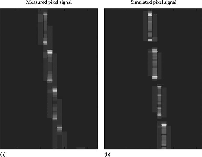
FIGURE 4.6
(a) Measured and (b) simulated slanted slit images for the indirect conversion GOS detector.
4.3.3 Properties of the MTF
Figure 4.7 shows the MTF comparison between an indirect and a direct conversion detector. The straight lines in red and blue are simulated curves, whereas the corresponding dashed curves show the respective ideal sinc functions. The indirect conversion detector shows a mid-frequency drop in comparison to the ideal sinc function. This is mainly due to optical crosstalk, which leads to a low-pass signal filtering in the detector. In principle, the mid-frequency drop can be recovered by appropriate inverse filtering at the expense of amplified electronic noise in the signal. For high and medium flux medical applications, this has no major impact. The signal-to-noise ratio is mainly affected in low-flux screening applications.

FIGURE 4.7
Modulation transfer functions for indirect conversion 1.2 mm pixel detector (dark gray) and direct conversion 450 μm detector (light gray). Dashed lines reflect the ideal sinc functions. (Reproduced from Wirth, S. et al., Simulations and measurements of the modulation transfer function of scintillator arrays, M06-257, IEEE Nuclear Science Symposium Conference Record, Honolulu, HI, 2008.)
In comparison to this, the direct conversion detector is close to the ideal sinc behavior. The remaining deviations are mainly due to fluorescence escapes between adjacent pixels. Despite the fact that the pixel aperture has been more than halved, charge sharing plays only a minor role compared to the effects of optical cross-talk. Note that in both detector systems, a small deviation in the zero frequency position is visible. This is due to the fact that fluorescence cross-talk leads to smaller signal contributions close to the pixel borders, effectively shrinking the pixel aperture.
4.4 Spectral Resolution
In nuclear physics and medical imaging applications like PET and SPECT, the spectral resolution of the detector is commonly described by the pulse height spectrum (PHS). A typical PHS of a CZT pixelized detector and a NaI Anger camera is shown in Figure 4.8. For x-ray applications, the detector has to register a whole range of input energies. Figure 4.9 shows a 80 and 140 kV tungsten tube spectrum. The generalization of the PHS to a range of input energies E leads to the detector response function (DRF), see [13].
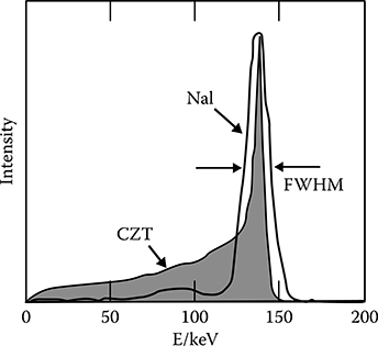
FIGURE 4.8
Pulse height spectrum (PHS) of CZT pixelized detector and a NaI anger camera. (Taken from Wernick, M.N. and Aarsvold, J.N., Emission Tomography, Academic Press, San Diego, CA, 2004.)
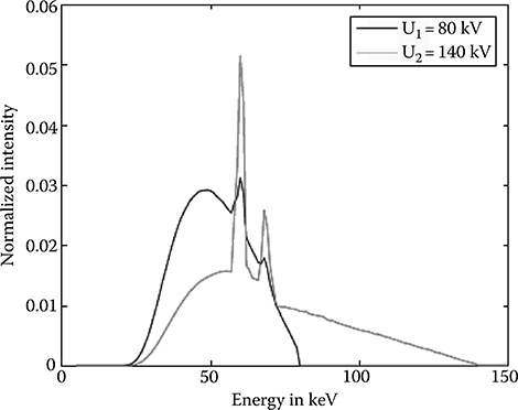
FIGURE 4.9
80 kV and 140 kV tungsten tube spectra.
4.4.1 Definition of the Detector Response Function
The DRF D(i,k)(E,E′) yields a probability density to measure the output energy E′ for an incoming quantum of energy E. The incoming quantum flux is directed at a central reference pixel. Its lateral position is equally distributed across the pixel area. The output energy is detected at a photo sensor pixel with the position (i, k). The pair (0,0) marks the center position, (1,0) the horizontal neighbors, (0,1) the vertical neighbors, etc. (see Figure 4.10).
The DRF allows us to express the statistics of the microscopic signal transport processes as a macroscopic probability function. We can simplify its variable dependencies for medical imaging applications. Here, the pixel-to-pixel variation of the projected anatomical input signal is usually below 1%. This is close to a flat-field irradiation of the detector. In this case, the mean signal cross-talk between pixels is symmetrical. We realize the flat-field approximation by irradiating the detector surface homogeneously. The simplified D(E,E′) function is used to describe the results.

FIGURE 4.10
Spatial indices (i, k) of the detector response function. The symmetry arises for pixels unaffected by border effects.
4.4.2 Comparison of the Detector Response Functions
The DRF of the indirect and direct conversion detector set-ups are shown in Figure 4.11a and b. In both cases, the probabilities are normalized to 1 for each input energy E. This leads to the respective color codings. Below 15 keV output energy E′, the electronic noise in the counting direct conversion detector dominates the output behavior. The respective range is omitted for better clarity.

FIGURE 4.11
Detector response function for (a) indirect conversion GOS detector, (b) direct conversion CZT detector.
The indirect conversion D(E,E′) in Figure 4.11a consists of the following structures:
Up to the gadolinium K-edge energy EK ∼ 50.2 keV, a linear branch E ∼ E′ is visible. Its broadening is explained by the energy conversion gain variance. The output energy peak has a tail toward higher output energies E′ for increasing input energy E. This light tailing effect is due to the fact that the light transport yield increases with the interaction depth, which in turn increases with the input energy E. Above the K-edge energy, a secondary branch occurs. The events are formed by absorption of the primary energy with a fluorescence energy loss to the surroundings. The corresponding reabsorbed fluorescence events are found in the third, approximately vertical branch starting at around 50 keV output energy. Its slight inclination is again due to the increase of the interaction depth with input energy. The overall absorption probability of the quanta is reduced with increasing input energy E. The low energy output events including Compton and Rayleigh scatter depositions are not shown, see [13] for a more detailed discussion of these effects.
The direct conversion detector D(E,E′) in Figure 4.11b has a more pronounced linear branch. Its stronger relative signal content is explained by the about two times higher intrinsic conversion gain of CZT and the reduced depth-dependency due to the small pixel effect. The fluorescence branches appear at the lower Cd, Zn, and Te fluorescence energies of 23–28 keV. The differential branches are consequently closer to the main linear branch. Charge sharing events create a low-energy tail increasing toward lower output energies and overlapping with the fluorescence branches.
The spectral behavior described by D(E,E0) has consequences for both detector schemes. In the following, we consider the cases of an integrating indirect conversion detector and a counting direct conversion detector as prominent examples.
4.4.3 Integrating Indirect Conversion Detectors
For integrating indirect conversion detectors, it has been shown that the output signal variance increase leads to a Poisson excess noise [13]. Following the work by Rabbani et al. [24], a formula for the noise amplification is established as

FIGURE 4.12
Generalized Swank factor f(E). (Reproduced from Heismann, B.J. et al., Nucl. Inst. Meth. Phys. Res., A, 591, 28, 2008.)
where
α(E) is the quantum detection efficiency
<E′> is the average output energy
σ(E′) is the output energy variance
f(E) is a generalized energy-dependent Swank factor
The Poisson excess noise shown in Figure 4.12 is more pronounced around the K-edge. A noise increase of about 15% is visible. This is due to the fact that the output signal variance increases strongly beyond the K-edge. For continuous input spectra, a typical excess noise of 5%–10% can be estimated, depending on the input spectra and the patient attenuation.
4.4.4 Counting Direct Conversion Detectors
For a counting direct conversion detector, we can distinguish between the full energy resolution required in SPECT or PET and the binned energy resolution required for dual-energy CT or radiography. In the case of full energy resolution, D(E,E0) contains directly the normalized PHS for specific input energies.
In the following, we focus on the case of a two bin energy resolution. Like shown in Figure 4.13, this is commonly achieved by using two threshold levels in the electronic read-out. The first threshold Eth1 discards noise events. The second threshold Eth2 separates the output energy range into two separate bins. The diagonal rectangular sections mark the quanta events, which are correctly assigned. The lower right region contains high-energy bin primary events, which are falsely assigned to the low-energy bin.

FIGURE 4.13
Schematics of energy binning for the detector response function of Figure 4.11a. Two energy threshold levels Eth1 = 15 keV, Eth2 = 55 keV are used.
Figure 4.14 shows the consequence of the low-energy shift. We have assumed a 140 kV tungsten x-ray tube input spectrum, see the shaded gray curve. The two detected spectra in the respective energy bins are given by the two straight curves.
Two effects are visible: First, the low-energy detected spectrum loses low-energy events. This is due to the fact that fluorescence events can carry away enough energy from a primary event to reduce the detected energy below the first energy threshold. Second, the two detected spectra overlap signifi-cantly. When we normalize both detected spectra to 1, we obtain the system weighting functions of the two energy bins. The overlap reaches around 60% and is thus comparably larger than the 40%–50% overlap of dual kVp or dual-source CT [25]. This indicates that the dual-energy measurement capabilities of direct conversion detectors are significantly affected by low-energy shift mechanisms due to fluorescence.
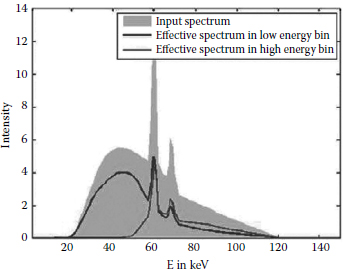
FIGURE 4.14
Detected spectra for a 140 kV tungsten input spectrum (shaded gray).
4.5 Conclusions
From the MTF results, we can deduce that the spatial resolution of semiconductor detectors is a clear potential benefit for medical imaging devices. The direct conversion of the primary x-ray field information into charge pulses omits the inter-pixel cross-talk of scintillator detectors almost completely. The direct conversion into charges demands for a strict control of electrical semiconductor defects. Low-flux screening applications in CT and other medical x-ray devices probably benefit the most from the improved spatial resolution as it requires less image filtering for the same obtained image resolution.
The intrinsic energy resolution of a counting detector read-out is a second potential benefit of a direct conversion semiconductor detector. For gamma-ray emission applications like SPECT and PET, the registered charge is a direct measure for the primary quantum energy. X-ray applications usually require only two or three energy bins defined by threshold energies. The DRF results indicate that CZT semiconductor detectors are prone to a shift of quantum detection to lower-energy bins due to interpixel fluorescence cross-talk.
The required spatial and spectral resolutions in semiconductor detectors are defined by the targeted medical device. For mammography and radiography detectors, spatial resolution is essential. CT relies on the detection of high x-ray fluxes at intermediate spatial and spectral resolution. SPECT and PET detectors mainly require a superior energy resolution. For each of these applications, detector parameters like the pixel size and the electronic readout have to be balanced accordingly.
References
1. G. F. Knoll, Radiation Detection and Measurement, 3rdedn. John Wiley & Sons Inc., New York, 2000.
2. I. M. Blevis, M. K. O'Connor, Z. Keidar, A. Pansky, H. Altman, and J. W. Hugg, CZT gamma camera for scintimammography, Phys. Med. Biol., 21(Suppl. 1), 56–59, 2006.
3. K. B. Parnham, S. Chowdhury, J. Li, D. J. Wagenaar, and B. E. Patt, Second-generation, tri-modality pre-clinical imaging system, M06-29, IEEE Nuclear Science Symposium Conference Record, Honolulu, HI, 2007.
4. D. J. Wagenaar, J. Zhang, T. Kazules, T. Vandehei, E. Bolle, S. Chowdhury, K. Parnham, and B. E. Patt, In vivo dual-isotope SPECT imaging with improved energy resolution, MR1-3, IEEE Nuclear Science Symposium Conference Record, Honolulu, HI, 2007.
5. E. Kraft , Counting and integrating readout for direct conversion X-ray imaging: Concept, realization and first prototype measurements, IEEE Trans. Nucl. Sci., 54(2), 383–390, 2007.
6. D. Moraes, J. Kaplon, and E. Nygard, CERN DxCTA counting chip, Proceedings of the 9th International Workshop on Radiation Imaging Detectors, Erlangen, Germany, 2007.
7. Y. Onishi, T. Nakashima, A. Koike, H. Morii, Y. Neo, H. Mimura, and T. Aoki, Material discriminated x-ray CT by using conventional microfocus x-ray tube and CdTe imager, M27-2, IEEE Nuclear Science Symposium Conference Record, Honolulu, HI, 2007.
8. J. P. Schlomka , Experimental feasibility of multi-energy photon counting k-edge imaging in pre-clinical computed tomography, Phys. Med. Biol., 53, 4031–4047, 2008.
9. S. A. Soldner, D. S. Bale, and C. Szeles, Dynamic lateral polarization in CdZnTe under high flux X-ray irradiation, IEEE Trans. Nucl. Sci., 54(5), 1723–1727, 2007.
10. E. Bolotnikov , Effects of Te inclusions on the performance of CdZnTe radiation detectors, R27-2, IEEE Nuclear Science Symposium Conference Record, Honolulu, HI, 2007.
11. G. S. Camarda, A. E. Bolotnikov, Y. Cui, A. Hossain, S. A. Awadalla, J. Mackenzie, H. Chen, and R. B. James, Polarization studies of CdZnTe detectors using synchrotron X-ray radiation, R27-3, IEEE Nuclear Science Symposium Conference Record, Honolulu, HI, 2007.
12. L. Abbene, S. D. Sordo, F. Fauci, G. Gerardi, A. L. Manna, G. Raso, A. Cola, E. Perillo, A. Raulo, V. Gostilo, and S. Stumbo, Study of the spectral response of CZT multiple-electrode detectors, N24-298, IEEE Nuclear Science Symposium Conference Record, Honolulu, HI, 2007.
13. B. J. Heismann, K. Pham-Gia, W. Metzger, D. Niederloehner, and S. Wirth, Signal transport in computed tomography detectors, Nucl. Inst. Meth. Phys. Res., A, 591, 28–33, 2008.
14. T. Michel , A fundamental method to determine the signal-to-noise ratio (SNR) and detective quantum efficiency (DQE) for a photon counting pixel detector, Nucl. Inst. Meth. Phys. Res., A, 568, 799–802, 2006.
15. I. A. Cunningham, Applied linear system theory, in: Handbook of Medical Imaging, Vol. 1, J. Beutel, H. L. Kundel, and R. L. van Metter, Eds. SPIE, Bellingham, WA, 2000.
16. J. Giersch and J. Durst, Monte Carlo simulations in x-ray imaging, Nucl. Inst. Meth. Phys. Res., A, 591, 300, 2008.
17. S. Agostinelli , G4—a simulation toolkit, Nucl. Inst. Meth. Phys. Res., A, 506(3), 250–303, July 2003.
18. J. Allison , Geant4 developments and applications, IEEE Trans. Nucl. Sci., 53(1), 270–278, February 2006.
19. B. J. Heismann, D. Henseler, D. Niederloehner, P. Hackenschmied, M. Strassburg, S. Janssen, and S. Wirth, Spectral and spatial resolution of semiconductor detectors in medical X- and gamma ray imaging, R03-1, IEEE Room Temperature Semiconductor Workshop, Dresden, Germany, 2008.
20. J. D. Eskin, H. H. Barrett, and H. B. Barber, Signals induced in semiconductor gamma-ray imaging detectors, J. Appl. Phys., 591, 647, 1999.
21. B. Kreisler, J. Durst, T. Michel, and G. Anton, Generalised adjoint simulation of induced signals in semiconductor X-ray pixel detectors, J. Inst., 3, 11, 2008.
22. S. Wirth, B. J. Heismann, D. Niederloehner, L. Baetz, W. Metzger, and K. Pham-Gia, Simulations and measurements of the modulation transfer function of scintillator arrays, M06-257, IEEE Nuclear Science Symposium Conference Record, Honolulu, HI, 2008.
23. T. Michel, Energy-dependent imaging properties of the Medipix2 x-ray-detector, Proceedings of Science on the 16th International Workshop on Vertex Detectors, Lake Placid, NY, 2007.
24. M. Rabbani, R. Shaw, and R. van Metter, Detective quantum efficiency of imaging systems with amplifying and scattering mechanisms, J. Opt. Soc. Am. A, 4, 895–901, 1987.
25. B. J. Heismann and S. Wirth, SNR performance comparison of dual-layer detector and dual-kVp spectral CT, IEEE Medical Imaging Conference Record, Honolulu, Hawaii, pp. 3280–3822, 2007.
26. M. N. Wernick and J. N. Aarsvold, Emission Tomography. Academic Press, San Diego, CA, 2004.