
12
Recent Developments of High-Performance PET Detectors
Hao Peng and Craig S. Levin
CONTENTS
12.3. High Photon Detection Sensitivity
12.4 Improved Spatial Resolution
12.4.1 Complex and Expensive Assembly
12.4.2 Reduced Scintillation Light Output
12.4.3 Compton Scatter and Multiple Interactions
12.4.4 Spatial Decoding for Block Detectors
12.4.5 High-Resolution PET Detector Developments
12.4.6 High-Density Data Acquisition Systems
12.5 Depth-of-Interaction Design
12.5.1 Multiple Crystal–Photodetector Layers
12.5.2 Single-Crystal Layer + Dual-Ended Photodetectors
12.5.4 Statistical Positioning with Monolithic Crystals
12.5.5 Dual-Layer Crystals of Offset Positions or Mixed Shapes
12.6 ToF PET and SiPM Detectors
12.6.2 Fast and High-Z Scintillation Materials
12.1 Introduction
Positron emission tomography (PET) is a noninvasive medical imaging tool widely used in both clinical and preclinical research. PET has proven its value in several areas such as cancer diagnosing and staging, assessing neurological diseases, myocardium viability evaluation in cardiology, as well as radiotherapy and chemotherapy monitoring [1–4]. In recent years, PET is also being actively used in small animal research using new molecular probes labeled with positron-emitting radionuclides. Applications using small animal PET include cell trafficking as cancer cells metastasize to different organs [5–8], gene delivery and expression in living animals [9,10], and low levels of endogenous messenger ribonucleic acid (mRNA) [11,12]. Advanced instrumentation, particularly high-performance detector designs, would help PET improve its image quality and enhance its molecular sensitivity for both clinical and small animal research. This chapter will focus on four aspects of the recent developments of high-performance PET detector designs: (1) high photon detection sensitivity, (2) improved spatial resolution, (3) depth-of-interaction (DoI) design, and (4) time-of-flight (ToF) PET and silicon photomultipliers (SiPMs).
12.2 PET: Basic Principles
Here we provide a brief description of the basic principles of a PET system and some terms to be used in this chapter. First, a tracer compound labeled with a positron-emitting radionuclide is injected to the object. The radionuclide then decays, and the resulting positrons subsequently annihilate with electrons after traveling a short distance within the object. Each annihilation produces two 511 keV photons traveling approximately in opposite directions, and these photons are detected by the detectors, which usually consist of scintillation materials, photodetectors, and front-end electronics. The signal of each photon from every pair coincidence event is processed individually for spatial, energy, and time information. For a pair coincidence event, if the energy of two photons stays within a preset energy window (∼20%–30% full width half maximum (FWHM) centered on the 511 keV photopeak) and the time difference stays within a preset time window (∼6–12 ns), a coincidence event will be registered and constitutes a line of response (LoR) for image reconstruction. In PET, there are three types of coincidence events [1,13,14]:
True coincidences (T) are the good coincident photon events where the LoR between the two coincident photons essentially passes through the points of emission.
Random coincidences (R) are a source of undesirable background counts that occur when two distinct nuclei each decay nearly at the same time and only one photon from each decay is detected within the time window. Random rates are reduced with lower detected single-photon count rate (single rate) and a narrower coincidence time window setting. It is desirable to have good coincidence time resolution so that a narrow time window may be employed to reject randoms without compromising photon sensitivity.
Scatter coincidences (S) are another undesirable source of background events that occur when one (or both) annihilation photon emitted from the same nucleus or single photons emitted from two separate nuclei undergoes one or more Compton scatter (CS) interactions inside the tissue before detection. Since CS causes a photon to lose energy, its effects can be reduced through the use of a narrow energy window setting around the 511 keV photopeak. It is desirable to have good energy resolution so that a narrow energy window may be employed to reject scattered coincidences without compromising photon sensitivity.
A widely used parameter, reflecting the signal-to-noise ratio (SNR) performance of a PET system in the context of three types of coincidences and optimum settings of both energy and time windows, is the noise equivalent count (NEC) [15] shown in Formula 12.1:
where
T, S, and R are the total number of true, scatter, and random coincidences, respectively
k is the number between 1 and 2, depending on the shape of phantoms/organs being imaged and the random estimation methods being used
A higher NEC at a given injection dose implies that a PET system is able to achieve better SNR and thus contrast-to-noise ratio (CNR) performance. In the following sections, we will focus on how to improve NEC and image quality through designing high-performance PET detectors and review a number of recent developments.
12.3 High Photon Detection Sensitivity
High photon sensitivity is a critical issue in PET instrumentation as it enables high statistical quality of acquired data, which is required to realize the potential of high spatial resolution [13,14,16]. High photon sensitivity also leads to a higher NEC in Formula 12.1 (i.e., due to Poisson statistics). For a PET system, the photon sensitivity is determined by two factors [14,17]: geometric efficiency (Eg) that reflects the solid angle coverage of the system and intrinsic coincidence detection efficiency (Ei) that is determined by the intrinsic properties of detectors (i.e., atomic number, density, thickness), crystal packing fraction, as well as the energy and time window settings. The overall system photon sensitivity (Es) is given by Formula 12.2:
The photon sensitivity is often quoted for a point positron source placed at the center of a PET system. For a standard clinical whole-body PET system (∼700–800 mm diameter bore), Es is normally around 0.5%–1% [18,19]; for a small animal PET system scanner (∼100–200 mm diameter bore), Es is around 1.0%–9.0% [20,21]. Eg is dependent on the total solid angle of a PET system, which can be increased either by moving detectors closer to the subject or by increasing the system coverage with more detectors. Several attempts have been made to address this issue including (1) extending the axial field of view (FoV) of a cylindrical system as deployed recently in Siemens Biography 64 TruePoint PET/CT whole-body scanner [22], (2) decreasing the system diameter, and (3) modifying the system geometry from cylindrical shape to other optimum geometries. There are several ways to increase Ei. The most straightforward way is to utilize scintillation materials with high Z and density (see Table 12.1), increasing the length of crystals, and/or packing them more tightly. However, longer crystals are associated with spatial resolution degradation toward the edge of FoV (also known as “parallax error”) and reduced light signal to be discussed later. In addition, Ei can be increased by using monolithic scintillation crystals [23–25], by stacking semiconductor detectors slabs such as cadmium–zinc–telluride (CZT) [26–31] and by using tapered crystal arrays [31,32]. Though not being widely used in PET as those scintillation crystals shown in Table 12.1, CZT is a novel solid detector and has great potential to be used for PET detector development (density 5.61 g/cm3; effective atomics number, 48; linear attenuation coefficient, 0.50 cm−1).
TABLE 12.1
Common Scintillators for PET Imaging

Consider a dual-panel breast-dedicated PET system based on CZT detector technology as shown in Figure 12.1. A simulation study indicates that for 4 cm panel separation and a point source, the system sensitivity can reach ∼32.5% at the center of FoV and can achieve >15% across the whole FoV for all three directions [33]. This is over an order of magnitude higher than the standard whole-body PET system (∼1% at the isocenter).
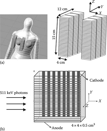
FIGURE 12.1
(a) Illustration of a dual-panel CZT-based PET system for breast cancer imaging. Each panel has dimensions of 4 × 12 × 15 cm3. Each detector module has dimensions of 4 × 4 × 0.5 cm3 with 25 μm inter-module spacing, giving a packing fraction of over 99%. (b) The cross-strip readout scheme for CZT detectors with sets of parallel anode and cathode strips in order to limit the number of electronic readout channels. (Adapted from Peng and Levin, Phys. Med. Biol., 55, 2761, 2010.)
The increased photon sensitivity of the CZT system is attributed to the dual-panel configuration, close proximity to the breast, high packing fraction of the CZT detectors (>99%), and the detector of 4 cm thickness seen by incoming 511 keV photons.
Another group studied tapered PET detectors and compared their performance against rectangular PET detectors [32], as shown in Figure 12.2. Essentially, these efforts intend to decrease the gaps both in-between crystal pitches and between detector modules. For small-diameter animal scanners based on ring geometry, these gaps can be a significant factor limiting the sensitivity. This study investigated a small animal PET scanner of an inner diameter of 6 cm and an outer diameter of 10 cm. The tapered crystals significantly reduce dead area in-between detector modules and thus increase the system packing fraction The traditional rectangular detector is a 14 × 14 array of 0.5 × 0.5 × 20 mm3 LSO crystals, while the tapered detector is a 14 × 14 array of 0.5 × 0.875 mm2 crystals (average height: 20 mm). The width of crystal elements is uniform in the axial direction but tapered in the transaxial dimension. Using the tapered arrays, the system achieves a photon sensitivity of ∼4.2% at the center of FoV, compared to ∼3.0% for the system with non-tapered crystals. Another novel approach to reducing the inter-module gaps that arise when arranging rectangular modules into a ring can be achieved by a box-shaped PET system as described in [17].
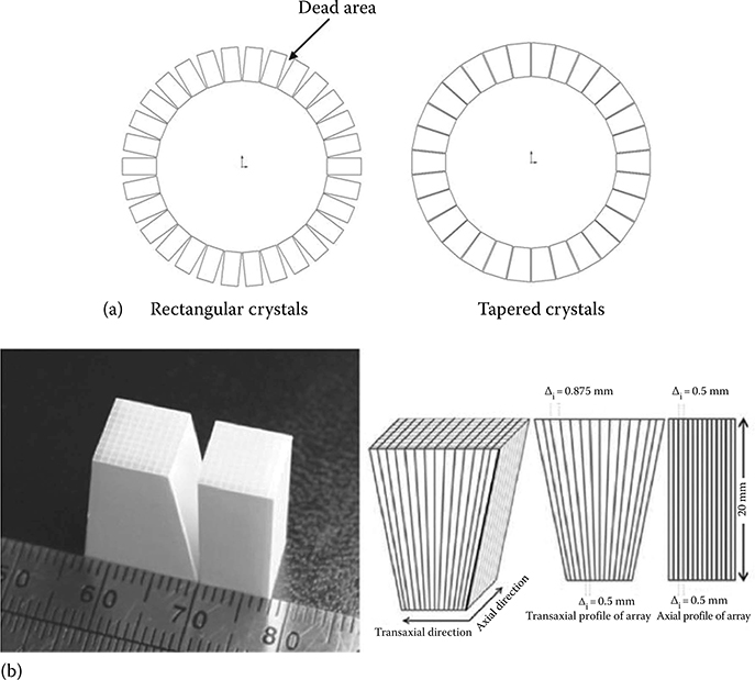
FIGURE 12.2
(a) Concept of using tapered crystals for small animal PET systems to reduce the dead area in-between detector modules (assuming a bore of 10 cm diameter, each detector module has a cross-sectional area of 1 × 1 cm2 and crystals of 2 cm height). (b) Photograph of a tapered LSO array next to a rectangular LSO array and illustration of the dimensions of the simulated tapered LSO array. Note that there is no tapering along the axial direction. (Adapted from James et al., Phys. Med. Biol., 54, 4605, 2009.)
It should be emphasized that Ei is also dependent on the coincidence time (typically 2× time resolution) and energy window (typically 2× energy resolution at 511 keV photopeak) settings in a PET system as only those events staying within the windows are recorded. In general, if other conditions remain the same, a system that exhibits better energy resolution and time resolution would have a larger Ei.
12.4 Improved Spatial Resolution
A framework with regard to PET spatial resolution (i.e., “point spread function,” PSF) has been proposed [34], based on the measurements with multiple whole-body PET scanners from different vendors [34]:
The contributions to FWHMPSF near the center of FoV as shown in Formula 12.3 include crystal size, annihilation photon acollinearity, positron range, reconstruction algorithm, and crystal-decoding factor. All factors are in the unit of mm (d, crystal pitch; D, scanner diameter; R, effective positron range). b is a factor empirically derived for PET block detectors and ranges from 0 to 2.2 depending on decoding algorithms.
The spatial resolution plays a critical role for PET image quality through contrast recovery as characterized by modulation transfer function (MTF), which is obtained by calculating the Fourier transforms of the PSF [13,16,35]. MTF is widely used to quantify a PET system's ability to recover the input contrast of objects at various spatial frequencies. A system with a flat MTF curve having a value near unity would faithfully reproduce the image object with ideal contrast recovery. Furthermore, such contrast (recovery) is linked to SNR and impacts the image quality of a PET system as indicated by Formula 12.4, also known as the Rose criterion that has been widely used in radiology for lesion detectability [36]:
where
CNR is contrast-to-noise ratio; contrast refers to the activity concentration ratio between lesions and background depending on tumor malignance and probe specificity
Npixels is the number of pixels contained by a lesion of given size (2-D case). The SNR is associated with the total counts detected, as well as the NEC value shown in Formula 12.1
The Formula 12.4 implies that using a PET system of high spatial resolution to detect smaller lesions is a challenging task. On one hand, high-resolution detector design is advantageous and can help improve contrast recovery. On the other hand, as Npixels decreases for smaller lesions, SNR and photon sensitivity (Formula 12.2) need to be significantly increased to maintain suffi-cient CNR. Such trade-off needs to be paid enough attention when designing high-resolution PET detectors and systems.
Based on the Formula 12.3, there have been several studies trying to investigate the spatial resolution limit of PET systems. Levin et al. found that for a point source of 18F in water-equivalent tissue determined by three blurring factors (positron range, photon acollinearity, and crystal pitch), 750 μm FWHM resolution is attainable with 1 mm crystal pitch and 20 cm system diameter [37]. In addition, Stefan et al. proposed a model for studying the intrinsic spatial resolution by considering the positioning uncertainty of high-energy photon inside various detector materials. The results indicate that 500 μm FWHM resolution is achievable if a 250 μm detector pixelation and 8 cm system diameter can be made [38]. Motivated by the simulation work, the group has successfully developed detectors of 500 and 750 μm LSO crystal pitches [39], as shown in Figure 12.3. Several major challenges faced by reducing the crystal pitch down to around 1 mm [1], as well as several promising solutions under investigation, are briefly summarized as follows.
12.4.1 Complex and Expensive Assembly
A major challenge of manufacturing PET detectors with smaller (e.g., <2 mm width) scintillation crystal elements is that cutting, surface treatments, and assembling crystals to make arrays are complex and expensive processes. Furthermore, optical reflectors are usually required to be inserted that typically have a minimum thickness about 50–75 μm. Assuming a single-crystal pitch of 250 μm is used, the optical reflectors in-between crystal pitches would degrade the packing fraction down to ∼60%–70%, significantly reducing the photon detection sensitivity.

FIGURE 12.3
(a) Photograph of a 20 × 30 crystal array of 0.43 mm crystal pitch and the resulting flood histogram. The array was read out by a Hamamatsu H7546 MCPMT that has 64 individual channels arranged in an 8 × 8 grid (grid pitch: 2.25 mm). Significant crystal overlapping in the flood map is noticed. (b) Crystal flood maps for two high-resolution arrays read out by PSAPDs. Four spatial channels at four corners of each PSAPD were used to position events using Anger logic. The device has an effective area of 1.0 × 1.0 cm2 and was cooled to −10°C to improve the detector’ SNR and crystal separation. The 1-D horizontal profile and the average PVR are shown for the flood maps obtained with cooling. (Adapted from James et al., Phys. Med. Biol., 54, 4605, 2009; Stickel et al., J. Nucl. Med., 48, 115, 2007.)
12.4.2 Reduced Scintillation light Output
A typical PET detector comprises long yet very crystal elements of low aspect ratio (i.e., width/height), which comprise the scintillation light collection. A weak scintillation light signal negatively impacts energy and time resolution and also limits the degree of spatial decoding. Light collection improvements can be made by proper treatment of the crystal faces, such as polishing or well-controlled etching, to enhance total internal reflection [40]. To address the issue of light loss, in 2 mm resolution PET systems built to date, relatively short (∼10 mm length) crystals are used [41,42]. However, this consequently compromises intrinsic PDE with a nearly 24% reduction (∼58% for a 10 mm long crystal versus ∼82% for a 20 mm one), based on the attenuation coefficient of LSO shown in Table 12.1.
This challenge can be addressed by using novel CZT detectors mentioned earlier. In such semiconductor detectors, the electron–hole pairs are directly involved in the electronic signal formation, instead of the relatively ineffi-cient process of creation/transportation of scintillation light in scintillator-based detector technology. As a result, compared to scintillator-based PET detectors, CZT detectors exhibit much better energy resolution for 511 keV photons [26–31].
12.4.3 Compton Scatter and Multiple Interactions
A 511 keV photon will interact with scintillation crystals or other type of detector materials and deposit its energy mainly through photoelectric effect (PE) and CS. If the detector elements are small, the scattered photons will usually escape into adjacent crystals before depositing their remaining energy, also known as multiple interactions. Multiple interactions occurring between adjacent crystals have been found to be a dominant source for the mispositioning of incoming 511 photons and contribute to the tails of the PSF [43,44]. This, in turn, degrades spatial resolution and contrast recovery. In general, the probability of photon scattering is higher for relatively low-Z, lower-density crystals such as GSO and CZT (see Table 12.1) and can also be significant in higher-Z crystals such as LSO, if crystal pitches are small [45]. The implication is that even though the utilization of a finer crystal pitch could improve the spatial resolution, the increased portion of multiple interactions due to the reduced crystal size might diminish that benefit while causing additional penalties such as light output loss.
12.4.4 Spatial Decoding for block Detectors
An important question is that how the reduced light output affects the spatial decoding. To explain this, the results of several recently developed PET detectors are presented in Figures 12.3 and 12.4, including (1) an LSO crystal array of 0.43 × 0.43 × 10 mm3 coupled to a position-sensitive photomultiplier tube (PMT) whereas the crystals in the flood map cannot be clearly resolved [46], (2) two LSO crystal arrays (0.5 and 0.7 mm pitch) coupled to position-sensitive avalanche photodiode (PSAPDs) [39], and (3) an 8 × 8 crystal LSO arrays coupled to a 2 × 2 large-area APD array through light multiplexing and Anger-logic positioning [47]. In Figure 12.3, at room temperature, crystals in the flood map of the 0.5 mm array are less resolved compared to the 0.7 mm array, due to the reduced light collection (i.e., smaller crystal pitch). As PSAPDs were cooled to −10°C, the quality of both flood maps improves since the devices have higher SNR at lower temperature. The peak-to-valley ratio (PVR), an important figure-of-merit widely used for block detector evaluation, is also shown for the two profiles of the flood maps. Higher PVR indicates that crystals are better distinguished, implying that the detector is able to achieve better spatial resolution in the context of PSF in Formula 12.4 (i.e., smaller b value). A flood map for a block detector of larger crystal pitch (2.5 mm) designed for a brain PET is shown in Figure 12.4. No cooling was applied and 64 crystals can be clearly resolved. The dependency of spatial decoding on the detector's SNR is demonstrated in the simulation results [47]. In essence, when a high-resolution crystal array is used with any type of multiplexing scheme, the reduced light collection will inevitably degrade the detectors’ SNR and thus the crystal separation (i.e., lower PVR), which make it less likely to achieve the theoretical resolution limit of 500 μm as predicated in [38].

FIGURE 12.4
(See color insert.) (a) Anger-logic PET block detector based on light multiplexing. A 2 × 2 array of large-area high-gain APDs was used. (b) Simulated flood maps under different SNR conditions of photodetectors (crystal dimensions: 2.5 × 2.5 × 20.0 mm3). Only one quadrant for the 8 × 8 array was simulated due to the symmetry. Significant degradation of the flood maps is observed as the SNR decreases. SNR refers to the ratio of the amplitude of 511 keV photopeak over the RMS noise of the detector when a single crystal is coupled directly to the photodetec-tor. (c) The block detector prototype comprising the LYSO array (crystal dimensions: 2.75 × 3.0 × 20.0 mm3), the optical diffuser (9 mm thickness), the APD array, and the highly compact custom readout electronics. The crystal flood map and the 1-D profile for the PVR analysis are shown. (Adapted from Peng and Levin, Phys. Med. Biol., 56, 3603, 2011.)
12.4.5 High-Resolution PET Detector Developments
Two novel detector designs that are capable of achieving high spatial resolution while not suffering from those limitations mentioned earlier are briefly described here. One approach is to use semiconductor detectors such as CZT or cadmium telluride instead of scintillation crystals [26–31]. Unlike scintillation crystals, semiconductor detectors directly sense the ionization signal created by the annihilation photon and do not create/transport scintillation light. Such direct conversion enables it to exhibit superior energy resolution of ∼1.5%–3.0% FWHM at 511 keV, compared to ∼10%–20% scintillator-based detectors. In addition, fine pixelation can be set by the segmented pattern of charge-collecting electrodes deposited on the crystal slab faces, rather than relying on cutting and assembling many miniscule crystal pixels [26,29]. For instance, to achieve high intrinsic spatial resolution of 500 μm, one can deposit the electrodes with a pitch that matches the desired spatial resolution, either in a cross-strip pattern or in a fully pixelated pattern.
Another approach is to read out the larger-area side faces of the crystals, rather than the small-area ends using very thin PSAPD photodetectors (Figure 12.5) [48–52]. In this new geometry, with the crystals/photodetectors orienting edge on with respect to incoming 511 keV photons, the average light path from the crystals to the photodetectors is greatly reduced and the light collection is nearly complete (>95%). This feature helps to achieve improved energy resolution (∼12%) and time resolution (∼2 ns) in addition to 1 mm spatial resolution.
One promising benefit of these two novel detector designs is their 3-D positioning capability. By recording the 3-D coordinates and energy deposition for every interaction, it is possible to use more intelligent positioning algorithms to better estimate the line of entrance of an incoming 511 keV photon in order to mitigate the effect of positioning errors due to intercrystal scattering, as discussed in Section 12.4.3. Such positioning algorithms may incorporate the physics of CS and/or a probabilistic formalism such as maximum likelihood to estimate the first interaction location with good accuracy [53], as well as retain events that are normally rejected such as single (unpaired) photons, tissue-scattered coincidences, and multiple-photon coincidences [54,55].
12.4.6 High-Density Data Acquisition Systems
Despite their superior performances, these novel CZT and LSO-PSAPD detectors face challenges in readout electronics developments. For example, a dual-panel breast-dedicated detector system based on LSO and PSAPD under development [51,56,57] will have more than 10,000 individual readout channels to be processed (Figure 12.5). On the other hand, the lower-gain and poorer-detector SNR of CZT and APD devices (compared to PMTs) prevent extensive multiplexing to be implemented to reduce the number of readout channels, either with charge multiplexing or light multiplexing [47]. Thus, a key bottleneck in the development of a PET system built from high-resolution 3-D positioning detectors is the development of high-density application-specific integrated circuits (ASICs) that are required to read out hundreds to thousands of densely packed detector channels [1,58].
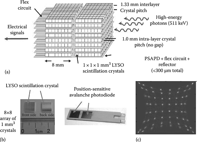
FIGURE 12.5
(a) Picture of an edge-on LYSO+PSAPD module including scintillation crystals, extra-thin PSAPD modules, and flex circuits. Each layer comprises two 200 μm thick PSAPD chips mounted on a 50 μm thick flex circuit. The flex circuit delivers bias to each PSAPD and enables readout of the four corner signals for positioning. (b) Picture of the thin module with two PSAPD chips mounted. Each dual-LYSO-PSAPD detector layer is oriented edge on so that incoming photons encounter a minimum of ∼2 cm thick of LSO with directly measured photon interaction depth (∼1 mm). (c) The crystal flood map of an 8 × 8 array of 1 × 1 × 1 mm3 LYSO crystals without cooling. (Adapted from Lau et al., Phys. Med. Biol., 55, 7149, 2010; Vandenbroucke et al., Phys. Med. Biol., 55, 5895, 2010.)
12.5 Depth-of-Interaction Design
A well-known problem in PET instrumentation is the parallax error, also known as the DoI problem, which impacts both spatial resolution and quantitative studies [59]. The framework proposed in Formula 12.2 does not take into such effect. A PET system typically comprises a circular arrangement of crystal arrays. The interaction of 511 keV photons with long crystal elements at oblique angles, as well as the penetration of 511 keV photons through multiple crystal elements, results in DoI blurring and leads to nonuniform spatial resolution.
The resolution blurring caused by the DoI effect can be mitigated if one can determine the photon interaction depth with improved accuracy. In general, DoI resolution has two types: discrete DoI and continuous DoI. The former one implies that crystals are physically segmented to independent units (similar to the pixilation through electrodes in CZT detectors). The latter implies that no physical segmentation is made and DoI is estimated/calibrated using collimated photon beams. DoI capability can be introduced for conventional scintillator–based PET detectors, and five representative DoI design schemes are summarized as follows. It is worthwhile pointing out that for those 3-D positioning detectors such as LSO+PSPAD- or CZT-based detectors examined earlier, the DoI capability has been inherently incorporated. For example, with edge-on PSAPDs configured on the sides of miniscule LSO crystal elements (Figure 5.5), the segmented crystals are able to achieve 1 mm intrinsic positioning capability along the DoI direction [26,29,48,49].
12.5.1 Multiple Crystal–Photodetector layers
The design consists of two or more crystal layers each read out by a layer of photodetector(s) [45,51,56,60,61]. As shown in Figure 12.6a, the DoI resolution is discrete and determined by the crystal segmentation of each layer. The advantage is that the overall detector performance is not compromised, as there is no optical and electric interference between the two layers. The drawback of this design is the increased number of electronic readout channels (2x more) and increased development cost.
12.5.2 Single-Crystal layer + Dual-Ended Photodetectors
This design employs a single-crystal layer read out by two photodetectors on both ends (Figure 12.6b). The depth information of the 511 keV photon inside the crystal is determined by the difference in the amount of light detected by the two photodetectors [62–64]. For an 8 × 8 array comprising 1 × 1 × 20 mm3 crystal pitches, average DoI resolution over all crystals and all depths is ∼3.5 ± 0.1 mm for the energy threshold E > 350 keV and ∼5.0 ± 0.1 mm for E < 350 keV when more CS events are included and thus degrade the photon positioning capability. Such design is also able to extract DoI resolution for even smaller arrays such as 0.5 mm and 0.75 mm pitch [38]. A minor problem about this design is that the light sharing and propagation along the long crystal (∼20 mm between the two photodetectors) may result in poor detector performance in terms of energy and/or time resolution, as well as the positioning nonlinearity near the faces of two photodetectors (i.e., nonuniform DoI resolution). In addition, as DoI resolution is directly dependent on the signal differences between the two photodetectors, the stability and calibration of detectors, particularly the gain variability between the two photodetectors, remain a challenge.
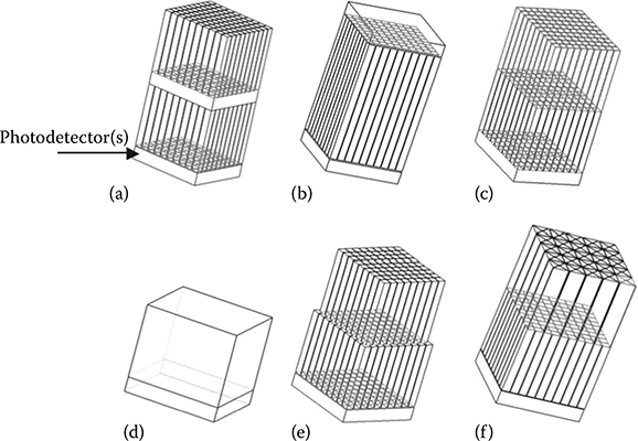
FIGURE 12.6
Illustration of several DOI detector design concepts for PET. (a) Dual-crystal photodetector(s) layers. (b) Single-crystal layer with photodetectors at each end. (c) Phoswich design with two types of scintillation materials. (d) Statistical positioning with a monolithic crystal block. (e) Dual-layer crystals with offset positions. (f) Dual-layer crystals of mixed shapes.
12.5.3 Phoswich Design
The phoswich detector comprises two different types of scintillation crystal materials read out by the same photodetector [65,66], as shown in Figure 12.6c. DoI capability is realized by pulse-shape discrimination based on the fact that the decay time constants of two scintillation materials are different (Table 12.1). In this design, complicated pulse-shape discrimination circuits are required to extract the timing difference between pulses originated from two types of materials. Ideally, the DoI resolution should be equal to the thickness of each crystals layer as in the design 5.1. However, several factors could degrade the DoI capability, including the limited decay time difference between the two materials, the intrinsic timing fluctuation in signal from each layer and electronics, multiple interactions involving both layers, as well as the light loss at the interface between the two crystal layers of different refractive indices. Nevertheless, such design has demonstrated good performance, and a commercial system based on such design is the GE small animal PET scanner (LYSO, 40 ns decay time, and GSO, 60 ns decay time).
12.5.4 Statistical Positioning with Monolithic Crystals
This design extracts the DoI information based on monolithic crystals and statistical modeling [67–69]. As shown in Figure 12.6d, a monolithic crystal block of relatively large size is read out by either individual photodetector(s) or position-sensitive photodetector(s), which can be coupled to either the entrance surface or the exit surface. In essence, the spatial resolution in the cross section of the crystal is obtained in the same manner as that in detectors without DoI capability. While in the DoI direction (the direction along which 511 keV photons enter the crystal), the DoI resolution is determined based on the light output intensity and light spread profile that both depend on the depth of photon interaction. Several algorithms have been developed for this design, including maximum likelihood and mean square error [67–69].
Despite the simplicity implied by the use of a single monolithic crystal layer, the complexity of this design lies mostly in the algorithms and calibrations. For instance, a set of experiments has to be done by irradiating the detector with 511 keV photon beams at a series of known positions and angles of incidence. Moreover, this design is subjected to the degeneracy of positioning near corners and edges of the crystal, where the spatial resolution is inferior compared to that near the center of the crystal. Nevertheless, such design has several attractive benefits besides the DoI capability: First, the use of monolithic crystal avoids complicated crystal cutting and assembly; second, it gets rid of dead area in-between crystal pitches and thus increases the photon detection sensitivity; and third, no extra optical interface, and therefore no light loss, is introduced as in other designs.
12.5.5 Dual-layer Crystals of Offset Positions or Mixed Shapes
In this design, two layers of crystals (same material) are involved and are read out by only a layer of photodetectors(s). As the top and bottom layers of crystals have different light output profile, their positions can be extracted accordingly. For instance, one method is to offset the top layer by half of the crystal pitch with respect to the bottom layer as shown in Figure 12.6e [70]. For illustration only, the top layer of a 9 × 9 array and the bottom layer of a 10 × 10 array are shown. Another design consists of two crystal layers built from crystals of different shapes, and more details are provided in Figure 12.7. Each layer is built from small modules and each module comprises eight crystals (four crystals for each layer). Note that the dimension of the base of a triangular crystal is twice that of the pitch of rectangular crystals. Here the light sharing is dependent on the crystal shape. For instance, the triangular crystals in the top layer form a special light-focusing pattern that enables their differentiation from the bottom layer of square crystals. This design provides discrete DoI and does not double the number of photo-detectors. Moreover, it does not require complicated readout electronics that are necessary in a phoswich design. However, one potential limitation may stay in the complexity and relatively high cost in manufacturing triangular-shape crystals.
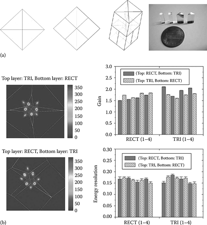
FIGURE 12.7
(a) DOI design using two layers comprising triangular (TRI) and rectangular (RECT) crystal elements. Each module consists of four triangular crystals (top layer) and four rectangular crystals (bottom layer). The picture of individual crystal segments is shown. (b) The flood histograms of a basic module (comprising eight crystals) are shown for two configurations (rectangular crystals at the top layer or at the bottom layer). The gain (in voltage) and the energy resolution FWHM after the individual crystals were segmented from the flood histograms and analyzed. No significant performance difference is observed between crystals in the two layers.
12.6 ToF PET and SiPM Detectors
12.6.1 Time-of-Flight PET
The history and recent progress of ToF-PET instrumentation are briefly reviewed here. By accurately measuring the arrival time of two 511 keV annihilation photons, the location of their emission points can be constrained. Though this constraint is not tight enough to avoid the image reconstruction or improve the spatial resolution, it can significantly reduce the statistical noise in the reconstructed images [71–74]. The SNR improvements are due to the following reason: In a non-ToF PET, the noise from all pixels along a given LoR is correlated, while in a ToF PET, the statistical fluctuations from the data along a LoR are constrained to a reduced number of image pixels, as illustrated in Figure 12.8. The framework developed for the SNR benefit of a ToF PET is given by Formula 12.5 [75,76]:
where
Δx is the position uncertainty
c is the speed of light
Δt is the time difference (related to the time resolution of PET detectors)
D is the size of the object being imaged

FIGURE 12.8
(a) In conventional PET, the source of the activity is localized to a LoR between a detector pair (i.e., two measured photons). (b) In ToF PET, timing information is used to restrain the source of the activity to a segment of the LoR. (Adapted from Moses, Nucl. Instrum. Methods Phys. Res. A, 580, 919, 2007.)
For example, for a time resolution of 500 ps that is currently achievable with fast scintillators and PMTs, Δx is ∼7.5 cm long. For an imaging object of 40 cm diameter, the SNR improvement is ∼2.3 and G is about 5.3. However, for small animal PET, with the coincidence time resolution of current detector technologies and small size of objects (e.g., ∼2–5 cm bore diameter), no SNR improvement is expected.
Back to the time the ToF concept was introduced in the 1980s, PET systems were mainly used for brain and cardiac imaging, whereas resolving small lesions and improving SNR were not deemed critical. However, the ToF PET has regained more research and clinical attention as PET increases its role in oncology nowadays. Several simulation and experimental studies have been performed to predict the performance of ToF whole-body PET systems. Phantom studies with a LYSO-based commercial ToF-PET scanner (Philips Gemini TF PET/CT) indicate that ToF information not only increases the lesion detection ability by a SNR gain of 1.4–1.6 (10 mm diameter lesion within 35 cm diameter background) but also reduces the number of iterations required in statistical image reconstruction [77]. Clinical studies also provide promising results that a ToF PET is able to reveal/define structural details in colon cancer, abdominal cancer, and lymphoma [77]. Currently, a number of ToF-PET scanners are commercially available, including Philips (crystal: LYSO) [78], Siemens (crystal: LSO) [79], and GE (crystal: LYSO) [80]. All these systems exhibit a timing resolution of ∼550–600 ps FWHM.
Very recently, the feasibility study using Cherenkov radiators for a ToF-PET system has also been made, such as PbF2, PbWO4, and lead glass [81]. For inorganic scintillation crystals such as LSO and LaBr3, the intrinsic time resolution is limited by the temporal response associated with transition of electron–hole pairs between energy states (i.e., stimulation from ground states to excited states (1–2 ns) and decay from excited states back to ground states (20–40 ns)). Traditionally used in high-energy particle physics, a Cherenkov light–based detector is able to achieve the excellent timing resolution (∼5–100 ps) and emerges as a promising candidate for ToF-PET systems [81]. The analytical calculation shows that the light output at 511 keV is found to be around 10–25 for high-Z Cherenkov radiators and around 50–250 for low-Z Cherenkov radiators. This poses a serious challenge for light detection and requires novel photodetectors of superior detection efficiency and low dark counts, which might be beyond the capabilities of detector technologies currently available. Besides the light yield, light photons collected by the photodetector also depend on crystal geometry as mentioned in Section 12.4.2. For standard PET crystals of smaller aspect ratio (i.e., the ratio between the width and the height), light trapping inside the crystals is significant and thus reduces light output. This implies that only PbF2/PbWO4 crystals of much larger aspect ratio should be considered for this promising application.
12.6.2 Fast and High-Z Scintillation Materials
In 1980s, a number of PET systems incorporating ToF were built based on BaF2 or CsF as they are very fast scintillators. However, they are not suitable for PET detectors due to the low light output and low detection efficiency, as well as the lack of high-speed electronics to perform accurate timing measurements. There has been renewed interest in ToF PET over the past few years [76,82], thanks to the availability of newly developed fast scintillators, such as LSO, LYSO, and LaBr3 crystals. As shown in Table 12.1, these crystals have high light output (good for energy resolution and scatter rejection), fast decay time constant (good for time resolution and random rejection), as well as good stopping power (high atomic number). Besides commercial LYSO-based ToF-PET scanners, Philips has recently developed a ToF-PET system based on LaBr3 crystals [83], which have a faster decay time and higher light output than LSO or LYSO though a lower atomic number Z. Preliminary characterization indicates that an array of 4 × 4 × 30 mm3 LaBr3 (5% Ce) readout with large size PMTs could achieve a time resolution of ∼313 ps FWHM and an average energy resolution of 5.1% FWHM at 511 keV [84], compared to a timing resolution of ∼585 ps and an energy resolution of 11.5% FWHM for LYSO crystals [78]. Furthermore, other scintillation materials such as LaBr3 (Ce) with different cerium concentrations, CeBr3, and LuI3 (Ce) are also being investigated [76].
Besides the intrinsic properties of materials, other parameters are also important for detector designs for ToF-PET systems, such as crystal surface treatment and crystal height selection [85]. In conventional clinical PET detectors, relatively long crystals (e.g., 4 × 4 × 20 mm3 LSO crystal pitch) are coupled to the surfaces of PMTs through light guide. If a scintillation event occurs at the back of one detector/crystal but the front of opposing detector/crystal, the difference in prorogation time within crystals will cause additional blurring in the measured coincidence time spectrum [75]. Furthermore, the use of any light guide itself would also degrade the time resolution. In this regard, the detector design using dual-crystal layers + dual-ended photodetectors mentioned in Section 12.5.1 appears to be a promising solution, which can achieve good time resolution (i.e., less propagation time within each layer of crystal), good DoI resolution, and high sensitivity at the same time.
It should also be pointed out that there exists a potential benefit of NEC improvement due to the superior time resolution of fast scintillation crystals. The simulation of a LaBr3-based ToF-PET system shows that it is able to achieve higher NEC as defined in Formula 12.1 than that of a LYSO-based ToF-PET system [83,84]. On the other hand, such system exhibits inferior performance compared to the LYSO scanner in terms of photon sensitivity. The authors provide a possible explanation for such seemingly contradictory results that the lower sensitivity of LaBr3 is partially offset by its lower scatter and random fractions due to its superior energy resolution and time resolution. Nevertheless, it should be kept in mind that such NEC improvement is only possible with two modifications made: (1) The crystal thickness increases from 20 mm (LYSO) to 30 mm (LaBr3), and (2) the axial FoV increases from 18 cm (LYSO) to 25 cm (LaBr3).
12.6.3 SiPM Devices
12.6.3.1 Overview of SiPM Operation
Being available recently, SiPM is considered a very attractive photodetector technology for ToF-PET system development [86–92]. Each SiPM pixel, of size ranging from 1 to 3 mm, contains thousands of micro-cells. Each micro-cell has a pitch of ∼20–50 μm and operates in the Geiger mode, which is also called Geiger APD and single-photon avalanche diode (SPAD). SiPMs are capable of measuring extremely low-level light signals to the extent of single photon. Compared to PMTs, they offer the “solid-state” advantages such as low operating voltages, ruggedness, compactness, and immunity to magnetic fields. Examples of SiPMs are shown in Figure 12.9.
A very brief description of how SiPM works is provided as follows, and more details about its working principles can be found in [91,92]. Each micro-cell (inside a SiPM pixel) consists of a reversely biased p-n junction and responds independently to incident photons. Electron–hole pairs are formed inside the depletion layer and drift in the presence of a high electric field. When the bias voltage increases above the breakdown voltage, each electron–hole pair is able to trigger a self-sustaining avalanche multiplication process called Geiger discharge. As a result, the number of charge carriers generated no longer reflects the intensity of incident photons. This is a fundamental difference between APDs and SiPMs, similar to that between proportional counters and Geiger tubes in gas detectors. To suppress the self-sustaining process and protect the micro-cells from excess large current, a quenching mechanism through either passive or active circuitry is required. For the passive quenching scheme, a large resistor is connected in series with the micro-cell, and when a large current flows through, it results in a voltage drop that brings the bias across the junction below the breakdown voltage. While for the active quenching, more complex voltage and timing controlling units are to be used. After a short duration determined by the time constant of quenching circuits, the bias across the micro-cell recovers back to the breakdown voltage so that it is ready for detecting another radiation event. Behaving essentially in a binary mode, each micro-cell produces a charge output (Qcell) as shown in Formula 12.6:
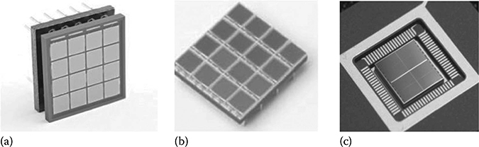
FIGURE 12.9
(a) Design of a 4 × 4 array of SiPM devices with ∼3.0 mm pitch from SensL (ceramic package). (b) Design of a 4 × 4 array of SiPM devices with ∼3.0 mm pitch from SensL (surface mount package). (c) Digital SiPM recently developed by Philips (a 2 × 2 array). Active area of each pixel is ∼3.8 × 3.3 mm2. Signal from multiple micro-cells within a pixel is digitally added. (Adapted from the technical notes from SensL and Degenhardt et al., IEEE Nucl. Sci. Symp. Conf. Rec., 2383, 2009; Frach et al. IEEE Nucl. Sci. Symp. Conf. Rec., 1959, 2009.)
where
Ccell is the micro-cell's capacitance
Vbias is the applied voltage
Vbreakdown is the breakdown voltage for the p-n junction (∼10–70 V)
The gain of a micro-cell is approximately 105–107, very comparable to that of PMTs. Finally, a number of micro-cells are connected to a common readout line, and the summation of output of individual microcells provides the amplitude information of incoming signals.
Another important parameter of SiPM devices is photon detection effi-ciency (PDE) shown in Formula 12.6. PDE is dependent on three terms: fill factor (FF), probability of Geiger discharge (PGeiger), and quantum efficiency (QE). The fill factor is the ratio of active areas of micro-cells to the total area of a single SiPM pixel. PGeiger depends on the location of electron–hole pairs within the depletion layer, as well as the strength and shape of the internal electric field. QE is strongly wavelength dependent, and a higher QE in blue region is desired for PET, due to the wavelength of scintillation light photons. Typical values of PDE for commercial SiPM devices are 20%–30% [92], which are also comparable to that obtained with PMTs.
A detailed comparison among three detector technologies (PMT, APD, and SiPM) for PET can be found in [91]. In brief, SiPM provides a number of advantages for PET instrumentation. First, its small pixel size (∼1–3 mm) enables detectors to achieve high spatial resolution, similar to those detector designs based on CZT and APD described earlier. Second, its high gain results in good detector SNR and eliminates the need for subsequent stages of amplification. Third, the output pulse of each micro-cell has a well-defined shape (i.e., both rising edge and amplitude), which is beneficial for accurate timing pick off [91]. A number of recent PET detector designs deploying SiPMs can be found in [91–96]. In particular, recent studies show that a time resolution of 237 and 240 ps (FWHM) is achieved for LaBr3 [93] and LYSO [94] crystals of 3 × 3 × 20 mm3 pitch, respectively.
Generally speaking, when the available space for accommodating detectors is a concern or when detectors need to work inside strong magnetic fields such as PET/MR systems, solid-state detectors such as APDs and SiPMs are preferred. On the other hand, when superior time resolution is desired as for ToF PET, PMTs and SiPMs are preferred over APDs as the latter suffer from relatively lower gain (lower SNR) but larger parasitic capacitance. However, whether SiPMs are able to achieve improved intrinsic time resolution over PMTs requires further investigation.
12.6.3.2 Digital SiPM
The SiPM operation described in the last section is also called analog SiPM, as each pixel processes analog output from many micro-cells through a common readout line and add them together. Subsequently, the output from each pixel is then digitized and processed for obtaining energy and time information. For a PET system consisting of thousands of channels, this becomes a very challenging task and requires the use of dedicated ASICs as discussed in Section 12.4.6. Such architecture faces a few potential challenges including [97,98] (1) expensive power-consuming electronics; (2) signal deterioration due to large parasitic of on-chip interconnect, bond wires, and external load; and (3) susceptibility to electronic noise and temperature variations that are typical characteristics of individual micro-cells.
To address these challenges, a novel design concept of SiPM emerges very recently, known as digital SiPM, and it is implemented in the complementary metal oxide semiconductor (CMOS) process. On one hand, CMOS sensors offer the promise of ultralow-power, low-cost, high-yield, and reliable deliv-erables [99–102]. On the other hand, by integrating micro-cells with the CMOS processes, it is possible to monolithically integrate the detector onto the same substrate as complex electronics required for quenching, analog-to-digital converter (ADC), time-to-digital converter (TDC), and data storage/transfer.
The architecture of a digital SiPM is illustrated in Figure 12.10. Each SiPM pixel comprises an array of micro-cells operating in Geiger mode. A logic circuit is attached to each micro-cell, allowing the micro-cell to capture, store, and output exactly one photon at a time. The CMOS inverter connected to the anode is designed to generate a high-speed asynchronous trigger and a slower synchronous data output signal, which are then transferred to other function blocks such as ADC and TDC for energy and timing information. To meet different requirements of spatial resolution, the output of ADC/TDC can be read out at either micro-cell level (i.e., for fluorescence lifetime imaging microscopy (FLIM) applications) [103,104] or pixel level (i.e., for ToF-PET applications).
The benefits of digital SiPMs over analog SiPMs are expected to be low dark count rate (DCR), high yield due to suppression of faulty micro-cells, improved timing performance, improved temperate stability, and no additional readout electronics such as ASICs required. Philips has recently demonstrated the feasibility of using digital SiPMs for PET applications [97,98], as shown in Figure 12.9. One thing worth mentioning is that the device is reported to be capable of achieving a time resolution of 170 ps FWHM, for a single LYSO crystal of 3 × 3 × 5 mm3. At the time of writing, the digital SiPM device is not yet commercially available though it has stimulated great interest in the community and is deemed to become the next-generation detector technology for PET instrumentation.

FIGURE 12.10
(a) Diagram of a digital SiPM with integrated ADC and TDC) functions. (b) Cross section of proposed SPAD structure with a novel guard ring implemented in standard 130 nm CMOS technology. SCR, space-charge region, and STI, shallow trench isolation. The novel guard ring structure is designed to suppress PEB. By violating the design rules of the standard CMOS technology and placing an n-well within the p-well, the edges of the junction are connected to two n-well guard rings that have lower doping than the n+ layer. Furthermore, by using a deep n-well layer, a p-well can be isolated from the substrate for minimizing DCR. The breakdown voltages at two junctions (11.3 and 9.4 V) are also shown, respectively. (Adapted from Palubiak et al., IEEE Sens. J., 11, 2401, 2011.)
In the following, the CMOS sensor fabrication and in-pixel circuitry integration are briefly discussed. Note that the micro-cell will be used interchangeably with SPAD hereafter, since the latter one has been widely used in the community of CMOS sensor development.
12.6.3.2.1 CMOS Fabrication Process
SiPMs or SPADs are traditionally designed and manufactured using proprietary processes (i.e., beveled-edge and reach-through structures), which facilitate the fabrication of stand-alone sensors with large active area (∼ several 100 μm in diameter) [105–107]. However, these structures and associated manufacture processes are based on ultrapure silicon wafers and nonplanar technology, which inherently limit the fabrication yield and are not suitable for monolithic integration of processing circuits.
Designing an effective guard ring is a major challenge for CMOS sensor development. Inside a SPAD, the very strong electric field within the depletion region must be uniformly distributed along the p–n junction. Therefore, a SPAD needs to have a guard ring structure in presence to avoid premature edge breakdown (PEB). Early implementations consist of a p+ anode and n-well cathode, with a guard ring structure created using the lateral diffusion of two n-tub regions [108]. The use of relatively old 0.8 μm CMOS technology guarantees a clean fabrication process and relatively low doping levels. Driven by the needs for more complex electronics, the 0.35 μm CMOS technology was also investigated for the fabrication of SPAD arrays [109–111]. Recently, the use of more advanced deep submicron (DSM) CMOS processes and a number of novel guard ring structures were studied, and an example is provided here. As shown in Figure 12.10, by using a triple-well process and placing an n-well within the p-well (i.e., which violates standard CMOS design rules) [112], the edges of the junction are connected to two n-well guard rings that have lower doping than the n+ layer. Furthermore, by introducing a deep n-well layer, a p-well is isolated from the substrate to help minimize DCR. Also note that the reverse breakdown of the SPAD junction occurs at 11.3 V, while the parasitic junction of the p-well/deep n-well breaks down at 9.3 V. Therefore, 9.3 V is the maximum negative voltage allowed at the anode before the breakdown of the parasitic p-n junction occurs [112].
Another challenge associated with DSM CMOS process is DCR performance, which is largely dependent on doping levels, annealing and drive-in diffusion steps, and the presence of shallow trench isolation (STI) [113–115]. The DCR could be up to several hundreds of kHz for an active area of only a few microns. For example, an implementation with lower noise (60 kHz for an active area of 10 μm in diameter and excess bias of 0.5 V) exhibits PDE of as low as 2.5% [113]. With the same technology, another study reports that a SPAD with active area of 3 μm diameter presents a ∼100 Hz of DCR [114]. However, no precise characterization of the device is given, and the extremely small active area might be of no practical use. Furthermore, all these DSM CMOS implementations suffer from the tunneling effect due to high implant doping levels (>5 × 1017 cm−3) [115].
Besides the fabrication process, another active research direction is the quenching and recharging (resetting) scheme [116,117]. An important trade-off involved is between high speed (i.e., low dead time) and noise performance. Passive quenching and active recharging have been commonly deployed in early works. Its main advantages include the well-defined hold time before recharge and a fast quenching and recharge time, which are beneficial for after-pulsing suppression. To further reduce the dead time and suppress after-pulsing events if necessary, active quenching and active recharging circuits have also been studied [117]. Nevertheless, such tasks will pose a few additional challenges such as increased parasitic capacitance and reduced fill factor of the SPAD.
12.6.3.2.2 Digital SiPM with In-Pixel Electronics
As mentioned earlier, CMOS process can make the detector more compatible with digital circuits and minimize electronic noises. Such a benefit may consequently result in improved energy and time resolution and thus a higher NEC as shown in Formula 12.1. Furthermore, maintaining all analog processing within the detector can reduce the power consumption of data acquisition system and enable scaling up to larger arrays with high cost-effectiveness, which is especially useful for high-resolution PET systems that have thousands of channels.
A SPAD array containing 60 sensors on a chip area of 18 × 18 mm was reported using the proprietary process [118,119], where the diameter of SPADs ranges from 20 to 75 μm. The design is heavily pad limited, and most of the chip area is used for interconnecting. In addition, studies also indicate that a SPAD would suffer from increased after-pulsing and optical cross talk due to larger parasitic capacitance, if quenching electronics were not integrated into the chip [120]. The first integration of in-pixel circuits into a CMOS SPAD array was shown in [109], which consists of a 4 × 8 array containing quenching resistors and inverters using the 0.8 μm CMOS process. A larger array (32 × 32) fabricated with the same technology was also developed [121]. Unfortunately, due to the large transistor size in the old CMOS technology, very limited electronics were integrated, and only a single pixel of the whole array could be activated at any time. To address that limitation, the 0.35 μm CMOS technology was deployed to improve the performances of SPADs, allowing for the integration of large-scale on-chip electronics. For example, a 128 × 128 SPAD array with an on-chip bank of 32 TDCs for time-correlated imaging applications was presented in [122]. A 17-bit ADC has also been successfully implemented over a 2 × 7 SPAD array [123].
Despite a number of potential benefits, there exists a serious challenge for this promising detector technology: how to maintain high PDE and fill factor when in-pixel circuits are introduced to CMOS sensors. The continuous need for additional metal layers to improve interconnecting in modern CMOS process results in more complex optical stacks, which consequently decrease the PDE as shown in Formula 12.6. Meanwhile, when various designs of high-performance ADC and TDC are introduced, a significant amount of chip areas (and interconnection tracers) are to be occupied by those function blocks, which would further reduce the fill factor and PDE. All these challenges need to be taken into account when designing digital SiPMs to be deployed for PET detector development.
12.7 Conclusions
This chapter reviews current challenges of advancing PET detector technology and some recent developments. It focuses on four important aspects of PET instrumentation: high photon detection sensitivity, improved spatial resolution, DoI resolution, and ToF PET and SiPMs. Improved system geometry, novel semiconductor detectors, and tapered scintillation crystal arrays are able to enhance the photon detection sensitivity of a PET system. Novel 3-D positioning detectors are of great potential to be deployed in PET for achieving high spatial resolution better than 1 mm, such as CZT and PSAPDs. DoI capability enables a PET system to achieve uniform spatial resolution across the FoV and improve accuracy for quantitative studies. The availability of fast scintillation crystals such as LaBr3 and SiPM greatly advances ToF-PET development. In particular, the development of digital SiPM using the standard CMOS process has huge potential to be used as the next-generation detector technology for PET instrumentation. All these technology advances, together with new imaging probe molecules, will ultimately enhance the molecular sensitivity of PET and increase its role in both preclinical and clinical research.
Acknowledgments
We would like to thank Canadian Breast Cancer Foundation Grant (2011R00356), NSERC Engagement Grant (537661), and NSERC Discovery Grant (596000) for their financial support. The authors would also like to thank Dr. Jamal Deen at McMaster University for his insightful discussion on CMOS sensor development.
References
1. C.S. Levin. New imaging technologies to enhance the molecular sensitivity of positron emission tomography, Proc. IEEE, 96, 439–467, 2008.
2. S.S. Gambhir. Molecular imaging of cancer with positron emission tomography, Nat. Rev. Cancer, 2, 683–693, 2002.
3. U. Nestle, H. Weber, and A.L. Grosu. Biological imaging in radiation therapy: Role of positron emission tomography, Phys. Med. Biol., 54, 1–25, 2009.
4. M.E. Phelps. Positron emission tomography provides molecular imaging of biological processes, Proc. Natl. Acad. Sci., 97, 9226–9233, 2000.
5. N. Adonai Ex vivo cell labeling with 64Cu-pyruvaldehyde-bis (N4-methylthiosemicarbazone) for imaging cell trafficking in mice with positron emission tomography, Proc. Natl. Acad. Sci., 99, 3030–3035, 2002.
6. J. Wang and L. Maurer. Positron emission tomography: Applications in drug discovery and drug development, Curr. Top. Med. Chem., 5, 1053–1075, 2005.
7. J.V. Frangioni and R.J. Hajjar. In vivo tracking of stem cells for clinical trials in cardiovascular disease, Circulation, 110, 3378–3383, 2004.
8. F. Cao In vivo visualization of embryonic stem cell survival, proliferation, and migration after cardiac delivery, Circulation, 113, 1005–1014, 2006.
9. K. Shah, A. Jacobs, X.O. Breakefield, and R. Weissleder. Molecular imaging of gene therapy for cancer, Gene Ther., 11, 1175–1187, 2004.
10. G.D. Luker. Special conference of the American association for cancer research on molecular imaging in cancer: Linking biology, function, and clinical applications in vivo, Cancer Res., 62, 2195–2198, 2002.
11. D.J. Hnatowich. Observations on the role of nuclear medicine in molecular imaging, J. Cell. Biochem., 39, 18–24, 2002.
12. R. Pither. PET and the role of in vivo molecular imaging in personalized medicine, Expert Rev. Mol. Diagnost., 3, 703–713, 2003.
13. S.R. Cherry. Physics in Nuclear Medicine, 3rd edn. Philadelphia, PA: Saunders, 2003.
14. National Electrical Manufacturers Association. NEMA Standards Publication NU 2–2001. Performance Measurements of Positron Emission Tomographs, Rosslyn, VA: National Electrical Manufacturers Association, 2001.
15. S.C. Strother, M.E. Casey, and E.J. Hoffman. Measuring PET scanner sensitivity: Relating count rates to image signal-to-noise ratios using noise equivalent counts, IEEE Trans. Nucl. Sci., 37, 783–788, 1990.
16. M.E. Phelps, S.C. Huang, and E.J. Hoffman. An analysis of signal amplification using small detectors in positron emission tomography, J. Comput. Assist. Tomogr., 6, 551–565, 1982.
17. F. Habte, A.M. Foudray, P.D. Olcott, and C.S. Levin. Effects of system geometry and other physical factors on photon sensitivity of high-resolution positron emission tomography, Phys. Med. Biol., 52, 3753–3772, 2007.
18. J.L. Humm, A. Rosenfeld, and A. Guerra. From PET detectors to PET scanners, Eur. J. Nucl. Med. Mol. Imaging, 30, 1574–1597, 2004.
19. A. Alessio, P. Kinahan, P. Cheng, H. Vesselle, and J. Karp. PET/CT scanner instrumentation, challenges, and solutions, Radiol. Clin. North Am., 42, 1017–1032, 2004.
20. Q. Bao, D. Newport, M. Chen, D.B. Stout, and A.F. Chatziioannou. Performance evaluation of the Inveon dedicated PET preclinical tomography based on the NEMA NU-4 standards, J. Nucl. Med., 50, 401–408, 2009.
21. M.C. Huisman, S. Reder, A.W. Weber, and S.I. Ziegler. Performance evaluation of the Philips MOSAIC small animal PET scanner, Eur. J. Nucl. Med. Mol. Imaging, 34, 532–540, 2007.
22. D.W. Townsend, B. Jakoby, and M.J. Long. Performance and clinical work-flow of a new combined PET/CT scanner, J. Nucl. Med., 48(supplement 2), 437, 2007.
23. J. Joung, R.S. Miyaoka, and T.K. Lewellen. cMice: A high resolution animal PET using continuous LSO with a statistics based positioning scheme, Nucl. Instrum. Methods Phys. Res. A., 489, 584–598, 2002.
24. M.C. Maas Monolithic scintillator PET detectors with intrinsic depth-of-interaction correction, Phys. Med. Biol., 54, 1893–1908, 2009.
25. T. Ling, K. Lee, and R.S. Miyaoka. Performance comparisons of continuous miniature crystal element (cMiCE) detectors, IEEE Trans. Nucl. Sci., 53, 2513–2518, 2006.
26. J.L. Matteson, M.R. Pelling, and R.T. Skelton. CZT detectors with 3D readout for gamma-ray spectroscopy and imaging, Proc. SPIE, 4784, 1–13, 2002.
27. P. Vaska Studies of CZT for PET applications, IEEE Nucl. Sci. Symp. Conf. Rec. pp. 2799–2802, 2005.
28. F. Zhang, H. Zhong, D. Xu, and L.J. Meng. Feasibility study of using two 3D position sensitive CZT detectors for small animal PET, IEEE Nucl. Sci. Symp. Conf. Rec. pp. 1582–1585, 2005.
29. Y. Gu Study of a high resolution, 3-D positioning cross-strip cadmium zinc telluride detector for PET, Phys. Med. Biol., 56, 1563, 2011.
30. G.S. Mitchell CdTe strip detector characterization for high resolution small animal PET, IEEE Trans. Nucl. Sci., 55, 870–876, 2008.
31. Y.F. Yang Tapered LSO arrays for small animal PET, Phys. Med. Biol., 56, 139–153, 2011.
32. S.S. James and S.R. Cherry. Simulation study of spatial resolution and sensitivity for the tapered depth of interaction PET detectors for small animal imaging, Phys. Med. Biol., 55, 63–74, 2010.
33. H. Peng and C.S. Levin. Design study of a high-resolution breast-dedicated PET system built from cadmium zinc telluride detectors, Phys. Med. Biol., 55, 2761–2788, 2010.
34. W.W. Moses and S.E. Derenzo. Empirical observation of resolution degradation in positron emission tomographs utilizing block detectors, J. Nucl. Med., 34, 101, 1993.
35. H. Peng and C.S. Levin. Study of PET intrinsic spatial resolution and contrast recovery improvement for PET/MRI systems, Phys. Med. Biol., 57, 101–115, 2012.
36. A. Rose. Vision: Human and Electronic, New York: Plenum, pp. 21–23, 1973.
37. C.S. Levin and E.J. Hoffman. Calculation of positron range and its effect on the fundamental limit of positron emission tomography system spatial resolution, Phys. Med. Biol., 44, 781–799, 1999.
38. J.R. Stickel and S.R. Cherry. High-resolution PET detector design: Modeling components of intrinsic spatial resolution, Phys. Med. Biol., 50, 179–195, 2005.
39. S.S. James Experimental characterization and system simulations of depth of interaction PET detectors using 0.5 mm and 0.7 mm LSO arrays, Phys. Med. Biol., 54, 4605–4615, 2009.
40. S.R. Cherry Collection of scintillation light from small BGO crystals, IEEE Trans. Nucl. Sci., 42, 1058–1063, 1995.
41. S. Surti Design evaluation of A-PET: A high sensitivity animal PET camera, IEEE Trans. Nucl. Sci., 50, 1357–1363, 2003.
42. J. Uribe Signal characteristics of individual crystals in high resolution BGO detector designs using PMT-quadrant sharing, IEEE Trans. Nucl. Sci., 50, 355–361, 2003.
43. C.S. Levin Compton scatter and x-ray crosstalk and the use of very thin intercrystal septa in high resolution PET detectors, IEEE Trans. Nucl. Sci., 44, 218–224, 1997.
44. R. Lecomte, D. Schmitt, and G. Lamoureux. Geometry study of a high resolution PET detection system using small detectors, IEEE Trans. Nucl. Sci., 31, 556–561, 1984.
45. C.S. Levin. Design of a high resolution and high sensitivity scintillation crystal array for PET with nearly complete light collection, IEEE Trans. Nucl. Sci., 49, 2236–2243, 2002.
46. J.R. Stickel, J. Qi, and S.R. Cherry. Fabrication and characterization of a 0.5-mm lutetium oxyorthosilicate detector array for high-resolution PET applications, J. Nucl. Med., 48, 115–121, 2007.
47. H. Peng and C.S. Levin. Investigation of a clinical PET detector module design that employs large-area avalanche photodetectors, Phys. Med. Biol., 56, 3603–3627, 2011.
48. C.S. Levin Investigation of position sensitive avalanche photodiodes for a new high-resolution PET detector design, IEEE Trans. Nucl. Sci., 51, 805–810, 2004.
49. J. Zhang Performance characterization of a novel thin position-sensitive avalanche photodiode for 1 mm resolution positron emission tomography, IEEE Trans. Nucl. Sci., 54, 415–421, 2007.
50. K.S. Shah Positron sensitive avalanche photodiodes for gamma-ray imaging, IEEE Trans. Nucl. Sci., 49, 1687–1692, 2002.
51. F.W. Lau Analog signal multiplexing for PSAPD-based PET detectors: Simulation and experimental validation, Phys. Med. Biol., 55, 7149–7174, 2010.
52. Y. Wu A study of the timing properties of position-sensitive avalanche photodiodes, Phys. Med. Biol., 54, 5155–5172, 2009.
53. G. Pratx and C.S. Levin. Bayesian reconstruction of photon interaction sequences for high-resolution PET detectors, Phys. Med. Biol., 54, 5073–5094, 2009.
54. G. Chinn and C.S. Levin. A maximum NEC criterion for compton collimation to accurately identify true coincidences in PET, IEEE Trans. Med. Imaging, 30, 1341–1352, 2011.
55. C.S. Levin. Promising new photon detection concepts for high resolution clinical and preclinical positron emission tomography, J. Nucl. Med., 53, 167–170, 2012.
56. A. Vandenbroucke Performance characterization of a new high resolution PET scintillation detector. Phys. Med. Biol., 55, 5895–5911, 2010.
57. Y. Gu Effects of multiple-interaction photon events in a high resolution PET system that uses 3-D positioning detectors. Med. Phys., 37, 5494–5508, 2010.
58. W.W. Moses OpenPET: A flexible electronics system for radiotracer imaging, IEEE Trans. Nucl. Sci., 57, 1–6, 2010.
59. M.E. Phelps. PET Molecular Imaging and Its Biological Applications. New York: Springer, 2004.
60. M. Rafecas A monte-carlo study of high resolution PET with granulated dual layer detectors, IEEE Trans. Nucl. Sci., 48, 1490–1495, 2001.
61. M. Rafecas Inter crystal scatter in a dual layer, high resolution LSO-APD positron emission tomography, Phys. Med. Biol., 48, 821–848, 2003.
62. Y. Yang Depth of interaction resolution measurements for a high resolution PET detector using position sensitive avalanche photodiodes, Phys. Med. Biol., 51, 2131–2142, 2006.
63. Y. Yang A prototype PET scanner with DOI-encoding detectors, J. Nucl. Med., 49, 1132–1140, 2008.
64. W.W. Moses, S.E. Derenzo, C.L. Melcher, and R.A. Manentet. A room temperature LSO/PIN photodiode PET detector module that measures depth of interaction, IEEE. Trans. Nucl. Sci., 42, 1085–1089, 1995.
65. J.B. Mosset Development of an optimized LSO/LuYAP phoswich detector head for the lausanne clearPET demonstrator, IEEE Trans. Nucl. Sci., 53, 25–29, 2006.
66. J. Seidel, J.J. Vaquero, and M.V. Green. Resolution uniformity and sensitivity of the NIH ATLAS small animal PET scanner: Comparison to simulated LSO scanners without depth-of-interaction capability, IEEE Trans. Nucl. Sci., 50, 1347–1350, 2003.
67. T. Ling, T.H. Burnett, T.K. Lewellen, and R.S. Miyaoka. Parametric positioning of a continuous crystal PET detector with depth of interaction decoding, Phys. Med. Biol., 53, 1843–1863, 2008.
68. M.C. Maas Experimental characterization of monolithic crystal small animal PET detectors read out by APD arrays, IEEE Trans. Nucl. Sci., 53, 1071–1077, 2006.
69. D.R. Schaart A novel, SiPM-array-based, monolithic scintillator detector for PET. Phys. Med. Biol., 54, 3501–3512, 2009.
70. N. Zhang Anode position and last dynode timing circuits for dual-layer BGO scintillator with PS-PMT based modular PET detectors, IEEE Trans. Nucl. Sci., 49, 2203–2207, 2002.
71. M.M. Ter-Pogossian Super PETTI: A positron emission tomography utilizing photon time-of-flight information, IEEE Trans. Med. Imaging, MI-1, 179–187, 1982.
72. W.H. Wong Characteristics of small barium fluoride (BaF2) scintillator for high intrinsic resolution time-of-flight positron emission tomography, IEEE Trans. Nucl. Sci., 31, 381–386, 1984.
73. N.A. Mullani Dynamic imaging with high resolution time-of-flight PET camera TOFPET-I, IEEE Trans. Nucl. Sci., 31, 609–613, 1984.
74. B. Mazoyer Physical characteristics of TTV03, a new high spatial resolution time-of-flight positron tomography, IEEE Trans. Nucl. Sci., 37, 778–782, 1990.
75. T.F. Budinger. Time-of-flight positron emission tomography: Status relative to conventional PET, J. Nucl. Med., 24, 73–78, 1983.
76. W.W. Moses. Recent advances and future advances in time-of-flight PET, Nucl. Instrum. Methods Phys. Res. A, 580, 919–924, 2007.
77. J.S. Karp Benefit of time-of-flight in PET: Experimental and clinical results, J. Nucl. Med., 49, 462–470, 2008.
78. S. Surti and J.S. Karp. Experimental evaluation of a simple lesion detection task with time-of-flight PET, J. Nucl. Med., 48, 471–480, 2007.
79. B.W. Jakoby, Y. Bercier, and M. Conti. Performance investigation of a time-of-flight PET/CT scanner, IEEE Nucl. Sci. Symp. Conf. Rec., pp. 3738–3743, 2008.
80. B. Kemp Clinical evaluation of a prototype time-of-flight PET/CT system, J. Nucl. Med., 50, 1513, 2009.
81. Y. Liang Feasibility study of sing cherenkov light crystals for time-of-flight PET Systems, IEEE Nucl. Sci. Symp. Med. Imaging Conf. Rec., pp. M16–73, 2012.
82. W.W. Moses. Current trends in scintillator detectors and materials, Nucl. Instr. Methods Phys. Res. A., 487, 123–128, 2002.
83. S. Surti, J.S. Karp, and G. Muehllehner. Image quality assessment of LaBr3-based whole-body 3D PET scanners: A Monte Carlo evaluation, Phys. Med. Biol., 49, 4593–4610, 2004.
84. M.E. Daube-Witherspoon The imaging performance of a LaBr3-based PET scanner, Phys. Med. Biol., 55, 45–64, 2010.
85. S.I. Ziegler Effects of scintillation light collection on the time resolution of a time-of-flight detector for annihilation quanta, IEEE Trans. Nucl. Sci., 37, 574–579, 1990.
86. D.J. Herbert The silicon photomultiplier for application to high-resolution positron emission tomography, Nucl. Instrum. Methods Phys. Res. A, 573, 84–87, 2007.
87. A. Nassalski Multi pixel photon counters (MPPC) as an alternative to APD in PET applications, IEEE Trans. Nucl. Sci., 57, 1008–1014, 2010.
88. D. Renker. New trends in photodetectors, Nucl. Instrum. Methods Phys. Res. A, 571, 1–6, 2007.
89. V.C. Spanoudaki and C.S. Levin. Investigating the temporal resolution limits of scintillation detection: Comparison between experiment and simulation, Phys. Med. Biol., 56, 735–756, 2011.
90. V.C. Spanoudaki and C.S. Levin. Scintillation induced response in passively-quenched Si-based single photon counting avalanche diode arrays, Opt. Express, 19, 1665–1679, 2011.
91. V.C. Spanoudaki and C.S. Levin. Photo-detectors for time of flight positron emission tomography (ToF-PET), Sensors, 10, 10484–10505, 2010.
92. E. Roncali and S.R. Cherry. Application of silicon photomultipliers to positron emission tomography, Ann. Biomed. Eng., 39, 1358–1377, 2011.
93. D.R. Schaart First experiments with LaBr3:Ce crystals coupled directly to silicon photomultipliers for PET applications, IEEE Nucl. Sci. Symp. Conf. Rec., pp. 3991–3994, 2008.
94. C. Kim, G.C. Wang, and S. Dolinsky. Multi-pixel photon counters for TOF PET detector and its challenges, IEEE Trans. Nucl. Sci., 56, 2580–2585, 2009.
95. A. Stewart Performance of 1-mm2 silicon photomultiplier, IEEE J. Quantum Electron., 44, 157–164, 2008.
96. M. Mazillo Silicon photomultiplier technology at STMicroelectronics, IEEE Trans. Nucl. Sci., 56, 2434–2442, 2009.
97. C. Degenhardt The digital silicon photomultiplier–a novel sensor for the detection of scintillation light, IEEE Nucl. Sci. Symp. Conf. Rec., pp. 2383–2386, 2009.
98. T. Frach The digital silicon photomultiplier–principle of operation and intrinsic detector performance, IEEE Nucl. Sci. Symp. Conf. Rec., pp. 1959–1965, 2009.
99. K. Yoon, C. Kim, B. Lee, and D. Lee. Single-chip CMOS image sensor for mobile applications, IEEE J. Solid-State Circuits, 37, 1839–1845, 2002.
100. F. Zappa, A. Lotito, and S. Tisa. Photon-counting chip for avalanche detectors, IEEE Photonics Tech. Lett., 17, 184–186, 2005.
101. D. Renker and E. Lorenz. Advances in solid state photon detectors, J. Instrum., 4, 04004, 2009.
102. R. Miyagawa and T. Kanade. CCD range-finding sensor, IEEE Trans. Electron. Devices, 44, 1648–1652, 1997.
103. R. Cubeddu Time-resolved fluorescence imaging in biology and medicine, J. Phys., 35, 61–76, 2002.
104. R.V. Krishnan Development of a multiphoton fluorescence lifetime imaging microscopy system using a streak camera, Rev. Sci. Instrum., 74, 2714–2721, 2003.
105. R.S. Goetzberger Avalanche effects in silicon P-N junctions.2. Structurally perfect junctions, J. Appl. Phys., 34, 1591, 1963.
106. PerkinElmer Optoelectronics (http://optoelectronics.perkinelmer.com) Technical notes: High speed APDs for Analytical and Biomedical Lowest Light Detection Applications.
107. M. Ghioni Progress in silicon single-photon avalanche diodes, IEEE J. Selected Topics Quantum Electron., 13, 852–862, 2007.
108. O. Elkhalili A 4 × 64 pixel CMOS image sensor for 3-D measurement applications, IEEE J. Solid State Circuits, 39, 1208–1212, 2004.
109. L.P. Stoppa, M. A CMOS 3-D imager based on single photon avalanche diode, IEEE Trans. Circuits Syst. I, 54, 8–12, 2007.
110. F.G. Tisa, A. Tosi, and F. Zappa. 100 kframe/s 8bit monolithic single-photon imag-ers, Proceedings of the 38th European Solid-State Device Research Conference, p. 4, 2008.
111. C. Niclass, C. Favi, T. Kluter, F. Monnier, and E. Charbon. Single-photon synchronous detection, Proceedings of the 34th European Solid-State Circuits Conference, pp. 114–117, 2008.
112. D. Palubiak High-speed, single-photon avalanche-photodiode imager for biomedical applications, IEEE Sens. J., 11, 2401–2412, 2011.
113. N. Faramarzpour, M.J. Deen, S. Shirani, and Q. Fang. Fully integrated single photon avalanche diode detector in standard CMOS 0.18-mu m technology, IEEE Trans. Electron. Devices, 55, pp. 760–767, March 2008.
114. M.A. Marwick and A.G. Andreou. Single photon avalanche photodetector with integrated quenching fabricated in TSMC 0.18 mu m 1.8 V CMOS process, Electron Lett., 44, 643–644, 2008.
115. S.M. Sze. Semiconductor Devices: Physics and Technology, New York: Wiley, 1985.
116. M.A. Marwick and A.G. Andreou. Fabrication and testing of single photon avalanche detectors in the TSMC 0.18 μm CMOS technology, 41st Annual Conference on Information Sciences and Systems, pp. 741–744, 2007.
117. M. Gronholm, J. Poikonen, and M. Laiho. A ring-oscillator-based active quenching and active recharge circuit for single photon avalanche diodes, Circuit Theory and Design, European Conference on, pp. 5–8, 2009.
118. F. Zappa SPADA: Single-photon avalanche diode arrays, IEEE Photonic Technol. Lett., 17, 657–659, 2005.
119. F. Zappa Single-photon avalanche diode arrays for fast transients and adaptive optics, IEEE Trans. Instrum. Meas., 55, 365–374, 2006.
120. I. Rech Optical crosstalk in single photon avalanche diode arrays: A new complete model, Opt. Express, 16, 8381–8394, 2008.
121. C. Niclass Design and characterization of a CMOS 3-D image sensor based on single photon avalanche diodes, IEEE J. Solid-State Circuits, 40, 1847–1854, 2005.
122. C. Niclass A 128 × 128 single-photon image sensor with column-level 10-bit time-to-digital converter array, IEEE J. Solid-State Circuits, 43, 2977–2989, 2008.
123. D. Stoppa Single-photon avalanche diode CMOS sensor for time-resolved fluorescence measurements, Sens. J. IEEE, 9, 1084–1090, 2009.