
10
Recent Advances in Capacitive Micromachined Ultrasonic Transducer Imaging Systems
Albert I. H. Chen, Lawrence L. P. Wong, and John T. W. Yeow
CONTENTS
10.4 CMUT–CMOS Integration Techniques
10.5.2 Large/High-Density 2D Array
10.1 Introduction
Ultrasound is one of the essential medical imaging modalities. The main advantage of ultrasound is its ability to penetrate tissues without the generation of harmful ionizing radiation. Therefore, it is not surprising that obstetric ultrasonography is the method of choice for prenatal care such as the monitoring of fetuses. Other benefits of using ultrasound technology include the availability of real-time results and portability of imaging units. On the other hand, ultrasound image quality may not be comparable to other modalities such as magnetic resonance imaging or computed tomography. In addition, it is difficult for ultrasound to penetrate bones or air, making the imaging of certain organs (e.g., the heart) a challenge. To overcome those challenges, researchers have been exploring various techniques to improve performance as well as to reduce the size of ultrasonic transducers in order to effectively perform in vivo imaging.
Conventionally, ultrasonic transducers comprised of piezoelectric materials such as lead zirconate titanate (PZT). These transducers rely on the piezoelectric effect, a mechanical deformation due to the presence of an electric field and vice versa, to generate and detect ultrasound. However, as micromachining technologies mature, a new type of ultrasonic transducer has emerged. Over the past decade, research in capacitive micromachined ultrasonic transducers (CMUTs) has demonstrated promising progress (see Figure 10.1). The microelectromechanical systems (MEMS)-based transducer was first constructed by the research group from Stanford University (Haller and Khuri-Yakub, 1994). These researchers envisioned a new type of transducer, fabricated using MEMS technology, for detecting cracks on aircrafts. These transducers had demonstrated excellent sensitivity and were able to offer superior resolution than traditional PZT transducers. It was soon realized that an even higher performance resulted when the transducer was immersed (Jin et al., 1998). As the imaging resolution is generally limited by the transducer, this had led to an incredible growth of interest toward CMUT research for medical imaging.
A scanning electron microscope image of CMUT cells is shown in Figure 10.2, while the schematic of a CMUT is shown in Figure 10.3. A typical CMUT cell consists of a movable membrane, a cavity, and two electrodes. If the membrane is electrically conductive, a layer of insulator is also required to prevent the two electrodes from shorting. The cavity is usually vacuum-sealed to enhance the performance and the reliability of the CMUT. The CMUT structure looks similar to a parallel plate capacitor, with the top electrode and the membrane forming the top plate and the bottom electrode and the substrate forming the bottom plate. CMUTs are actuated in a fundamentally different manner than PZT transducers. They operate like a condenser microphone: when provided with a voltage excitement and a fixed bottom plate, the top plate vibrates and hence transmits sound wave. Conversely, when sound waves hit the top plate, the membrane displaces and, in turn, changes the capacitance between the plates. During this receive event, the voltage across the electrodes is held fixed, so as capacitance changes, electrical current is produced. From this step onward, the rest of the imaging system varies little from a conventional ultrasound imager.

FIGURE 10.1
(a) Different CMUT designs can be made for different applications. Packing large number of ultrasonic transducers into a tiny area has never been easier! (b) Transducer array connected to electrodes demands packaging solutions. (c) Each CMUT cell is much smaller than the diameter of the human hair!
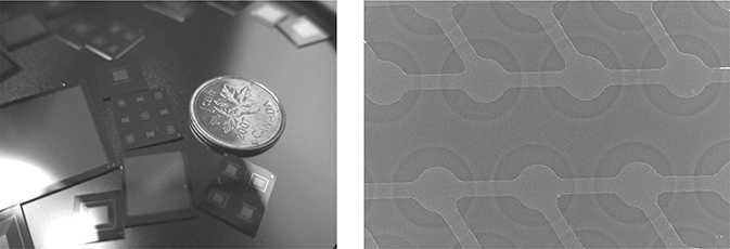
FIGURE 10.2
CMUT membrane diameter for a 10 MHz operation: 22 μm in diameter, 400 nm in membrane thickness, 11 μm in electrode diameter, and 140 nm in cavity depth. This 1D CMUT has 4140 cells per element.

FIGURE 10.3
Cross-sectional schematic of a CMUT cell.
CMUTs are fabricated using the same techniques as the common integrated circuit (IC) production. As a result, these novel transducers can be manufactured at a lower cost and with a higher yield. More importantly, standardized micromachining techniques allow CMUTs to be fabricated on ICs (CMUT on CMOS), producing tiny feature sizes. In other words, CMUTs are designed to be integrated with microelectronic circuits with ease—we will soon discuss why this is of major significance.
This chapter is an overview of recent advancements in CMUT systems. In the following section, we will discuss how CMUTs are fabricated and what design considerations are made. In Section 10.3, the main benefits of using CMUTs are presented. One of these benefits includes the effective integration of CMUTs with the complementary metal-oxide semiconductor (CMOS) technology—we will discuss this in Section 10.4. The applications of CMUTs are then presented in Section 10.5, while the challenges associated with the technology will be presented in Section 10.6.
10.2 Design and Fabrication
Given the similarities between a condenser microphone and a CMUT, one might wonder why the CMUT was not developed sooner. In fact, the main problem researchers faced was related to one of the main CMUT design parameters, the depth of the cavity or gap height. In order to generate an electric field large enough for the CMUT to be useful and avoid damaging the device, a small gap height in the range of micro- or nanometer is required. Thanks to the advances in micromachining technologies, such a small gap can now be easily achievable. When designing a CMUT, one should choose a small gap height to keep the bias voltage reasonable. On the other hand, the gap height should be large enough to allow room for the membrane to vibrate. Most of the time, however, the range of achievable gap height is also determined by the fabrication process.
Another important CMUT design parameter is the horizontal dimension of the CMUT membrane, or the diameter of the membrane in the case that the CMUT is circular. A bigger membrane area results in a lower resonant frequency, thus a lower ultrasound frequency. The ultrasound frequency is important because a higher frequency means a higher axial resolution in the resulting images. However, lower-frequency ultrasound has a better penetrability, so there is always a design trade-off. The size of the CMUT membrane is usually in the micrometer range for typical medical ultrasound frequency, which is in the MHz range. In order to generate sufficient energy, many CMUT cells are connected in parallel to form an element. The shape of the CMUT membrane is another key factor to be considered. Square- and hexagon-shaped membranes were reported to produce the maximum area efficiency of the device; but circular membrane is most often used in CMUTs because it generates the lowest local stress (Huang et al., 2003).
The materials used to construct the CMUTs also affect the device performance. A stiff membrane results in a higher ultrasound frequency but a lower signal amplitude because it takes more energy to vibrate. Silicon nitride and silicon oxide are two common materials for the CMUT membrane and dielectric layer (Logan and Yeow, 2009). They are used because of their mechanical properties and the fact that they can be easily grown on a silicon substrate using standard fabrication processes.
The most important CMUT fabrication step is the formation of the cavities. Different methods were proposed to form the cavities, but they can be categorized into two types: surface micromachining and bulk micromachining. Surface micromachining involves depositing the layers of the CMUT structure one by one, from the bottom to the top. The cavity is initially occupied by a sacrificial layer, which is then removed upon the completion of the structure. This step is also known as the releasing of the structure or the membrane. In order to allow etchant access to the sacrificial layer, etch holes are required on the top layers. Moreover, the sacrificial layer cannot be too thin; otherwise, the membrane may not be released properly. If a vacuum cavity is desired, the etch holes need to be sealed off. Bulk micro-machining involves fabricating the bottom electrode on one wafer and the top electrode on another wafer. The wafers are bonded together after the cavities are etched on one of the wafers; therefore, the process is also known as wafer bonding. Because the cavities are formed on the top layer before being covered by another wafer, very small gap heights can be achieved using wafer bonding. Bulk micromachining is the more popular choice of CMUT fabrication because more efficient structures can be realized using wafer bonding.
Since the membrane and top electrodes are susceptible to abrasion, an encapsulation layer is required to protect the device. Furthermore, this layer should insulate the electrical components from the environment while maintaining certain biocompatibility standards. More importantly, the insulating material should minimize any adverse impact on the CMUT's acoustic performance. In its working environment, an ideal encapsulating material will have a static Young's modulus low enough to allow the CMUT elements to pull in during DC excitation as well as a dynamic Young's modulus high enough to allow acoustic matching with water at ultrasonic frequencies. Currently, polydimethylsiloxane (PDMS) is favored as the viscoelastic material for depositing on the CMUT since it meets performance specification and is well characterized for modeling (Lin et al., 2011). Ideally, a thin coating is desired as it minimizes any acoustical effect on the CMUT but is impractical as it may be easily damaged by ablative force. Through modeling and experiments, a layer in the range of 150–300 μm is considered acceptable for meeting specifications (Lin et al., 2010). Figure 10.4 shows how the encapsulation layer fits with a 1D array device. The layer can be molded into a lens for better focusing.
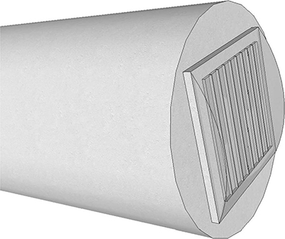
FIGURE 10.4
An encapsulation layer is typically required to insulate and protect the CMUTs. The encapsulation layer can also be molded into lens for 1D array.
10.3 Benefits
10.3.1 Wider bandwidth
Compared to a PZT transducer, the vibrating membrane of a CMUT is substantially thinner. As a result, a CMUT experiences a much higher damping that leads to a wider bandwidth, or less ringing. Imagine if ringing effect was significant in our ears, we would be hearing echoes and distorted sounds constantly and be unable to appreciate a symphony and clearly distinguish between notes! In short, it is extremely important to have a wider bandwidth in order to resolve spatially.*
One reason why PZT transducers are bulky, relative to CMUTs, is that an acoustic impedance matching layer is required. A structure's acoustic impedance is dependent on the material composite and also geometry. For any vibration energy to transfer efficiently between mediums, the impedance of the source medium should match the impedance of the medium of interest. An impedance mismatch creates inefficiency in the acoustic energy transfer and will introduce noise and heat. Although an impedance matching layer can be designed to minimize the inefficiency, any extra thickness will contribute to additional ringing effect.†
* To be more precise, a wider bandwidth improves the axial resolution but not so much the lateral resolution.
†A great read to understand PZT transducer design can be found in Diagnostic Ultrasound Imaging by Thomas L. Szabo (Szabo, 2004).

FIGURE 10.5
Comparison of imaging results between PZT array (left) and CMUT array (right). (a) Imaging of the carotid artery. (b) Imaging with the thyroid gland froma. Notice the increase in structural details of the CMUTs. (From Mills, D.M. and Smith, L.S., IEEE Symposium on Ultrasonics, pp. 568–571, 2003. Copyright IEEE with permission.)
In 2003, General Electric Global Research Center reported the first real-time CMUT probe with linear CMUT arrays. Compared to a benchmarking PZT probe, the CMUT images demonstrated improved anatomical border and texture information. Figure 10.5 shows the image comparison between PZT-based and CMUT-based imaging ultrasound probes (Mills and Smith, 2003). In 2009, Hitachi Medical Corporation reported the first successful com-mercialization of a CMUT-based array capable of 2D cross-sectional imaging (Hitachi Medical Corporation, 2009).
10.3.2 Smaller Pitch
In modern medical ultrasound imaging, it is common to focus sound with an array of transducer elements instead of a single element. Furthermore, electrical focusing, or phased-array focusing, is used to steer and focus the sound beam. The idea is to orchestrate pulses from each element in the array such that a maximum constructive interference can be created at a desired destination. As a result, the signal-to-noise ratio (SNR) can be increased as sound energies from multiple transducers are focused at a single point while any mechanical movement is eliminated. The latter property improves the scanning speed and accuracy when compared to traditional focusing typically requires lens and mechanical actuators for beam steering.
Eliminating mechanical movements is beneficial but phased array introduces a critical design constraint: to eliminate aliasing (also known as grating lobes in ultrasound terminology), which causes image blur, the array pitch must be less than half of the operating wavelength. The concept of grating lobes is illustrated in Figure 10.6. For high-frequency imaging, which is typically greater than 25 MHz, the pitch is required to be less than 30 μm. For PZT transducer fabrication, it is very difficult to achieve less than 40 μm in pitch due to limitations in the traditional dice-and-fill method. In contrast, from the standpoint of microfabrication (i.e., MEMS technology), micrometer-level feature size can be easily achieved. In conclusion, CMUTs are far less likely to encounter the grating lobe problem, thus better image quality.
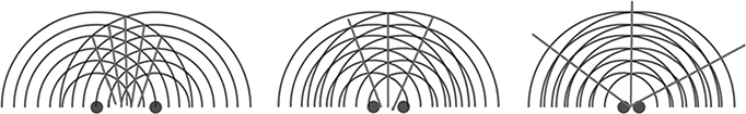
FIGURE 10.6
Ideally, the sound should focus at only one point. However, when transducers are far apart, constructive interference may occur at undesirable places and grating lobes occur.
10.3.3 IC Integration
Most medical ultrasonic imaging systems can be broken down into four parts: the ultrasonic transducers, the front-end circuitry, the cable, and the back-end processing unit. Since the transducers are typically encased in a housing that is remote to the processing unit, the raw signal received by the transducers can be significantly degraded due to cable capacitance. Therefore, front-end electronics must be incorporated with the transducers to maintain the signal integrity. Each transducer element has a dedicated transmitter and receiver circuit. The transmitter circuit typically includes a high-voltage switch to generate a large pulse, while the receiver includes an amplifier to enhance the measured signal.
It is difficult to package both the electronics and the high-density transducer array. Even though the CMOS technology can provide tiny ICs, it is still challenging to make the interconnections between individual elements and corresponding transmitter and receiver circuitry. (This is not true for CMUT technology but will be discussed shortly.) Consider a large array with 128 × 128 transducer elements; over 16,000 interconnections are needed to address each element individually; meanwhile the pitch size is constrained by the frequency. In catheter applications, although the element count is not high, interfacing the electronics is still challenging given the tiny workable area.
Traditionally, PZTs are diced into arrays with fine saws followed by the deposition of electrodes. The front-end components are fabricated separately and eventually soldered with the electrodes. However, at high densities and small surface areas, it becomes incredibly challenging to work with the traditional method. Thus, when the CMUT-on-CMOS process was demonstrated, it gave great hope to the future of ultrasound technology. The next section will discuss various CMUT and electronics integration methods.
10.4 CMUT–CMOS Integration Techniques
Although microfabrication can produce very tiny feature sizes (i.e., thin membranes and small pitches), there is a plethora of design constraints to be considered. For example, to ensure the membrane is bonded tightly onto the insulating material, high temperature is required. However, the electronics may be damaged in the high temperature. Therefore, some design trade-offs may be required. We will briefly discuss different ways of combining the CMUT with electronic circuits fabricated using the CMOS process.
10.4.1 CMUT in CMOS
CMUT and electronics are fabricated in parallel on the same wafer and under the same CMOS process (Cheng et al., 2009), as illustrated in Figure 10.7. This method reduces fabrication time and cost. However, the material type, the material properties, and the layer thickness of the CMUTs are subjected to the limitation of the CMOS process. This method is also not ideal for applications where a small transducer area is required.
10.4.2 Flip-Chip Integration
This process allows the CMUTs and the electric circuits to be optimized separately, followed by flip-chip bonding (Noble et al., 2001). This way, the high temperature for CMUT fabrication will be isolated from the CMOS fabrication. In addition, the total occupied area is minimized because both the CMUT and the CMOS circuits are stacked. However, to satisfy the requirements for flip-chip bonding, the CMUT design must have through-wafer vias (TWVs) such that both the top and bottom electrodes can be accessed by the bonding pads at the bottom of the wafer (Figure 10.8). As a result, this method is rather complex. Nonetheless, since flip-chip integration allows CMUT design optimization, it remains popular with current imaging research.

FIGURE 10.7
CMUT-in-CMOS process refers to the process where CMUTs and CMOS are fabricated on a single wafer in parallel.
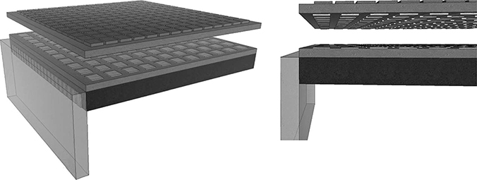
FIGURE 10.8
CMUT fabrication and CMOS process can be done separately followed by flip-chip soldering.
10.4.3 CMUT on CMOS
The most cost-effective method is the CMUT-on-CMOS process. Here, CMUT fabrication process is fabricated on top of the CMOS circuits (Gurun et al., 2011) (Figures 10.9 and 10.10), resulting in minimal in-plane area and minimal parasitic capacitance caused by electronic traces and interfaces. The main problem associated with this technique is that the fabrication temperature for the CMUTs is limited to protect the electronics. However, this process is still an active research area as steady improvements have been made on fabricating better CMUTs under low temperature.
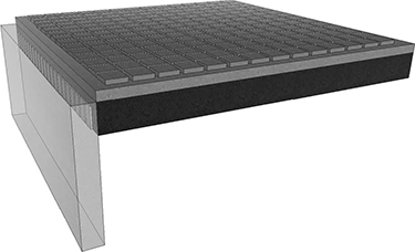
FIGURE 10.9
CMUTs can be built on top of CMOS. This creates a very tight packaging.

FIGURE 10.10
The application-specific integrated circuits (ASICs) can be seen (a) before the CMUT deposition (b). (From Gurun, G. et al., IEEE Transactions on Ultrasonics, Ferroelectrics and Frequency Control, 58–8, 1658–1668, 2011. Copyright IEEE with permission.)
10.5 Applications
The advantages of CMUT have shaped the technology to evolve into two main branches in terms of medical imaging applications. The first branch of research revolves around in vivo application where CMUTs are typically placed on the tip of catheters or endoscopes for intravascular-/intracardiac-like ultrasound imaging. Within this branch, packaging and interface engineering are the key factors in research. The second branch involves developing large and high-density 2D arrays to image large areas, typically from outside the body. Within this branch, the key factors include not only the two mentioned but also electronics simplification schemes. In this section, we will discuss the two branches, followed by the latest development in CMUT systems.
10.5.1 Small 2D Array
Intravascular ultrasound and intracardiac echocardiography (IVUS and ICE) imaging has been commercially available for over a decade. Angiography, the most widely used vascular imaging technique, cannot provide closeup anatomy of the lumen. By attaching ultrasonic transducers at the distal end of a catheter, the anatomy near the tip can be better perceived.
Traditionally, IVUS and ICE have side-looking apertures; therefore, imaging is performed radially. In recent years, engineers have been trying to implement forward-looking IVUS catheters that provide much more useful information such as plaque occluding the blood vessel. Most of the methods adopt a single piezoelectric transducer and some sort of mechanical actuators to redirect the sound beam. As discussed previously, mechanical actuation limits the frame rate and also introduces noise. In the realm of microfab-rication, where millimeter spacing is considered enormous, phased-array imaging becomes a possibility because a CMUT array can be easily placed at the face of the tip instead of at the outer surface, eliminating the need for mechanical movement during a scan. In fact, several research groups have demonstrated ring array CMUT catheters where a hollow center is kept (see Figure 10.11) for fitting an ablation device capable of burning plaque occluding the vessels using high-intensity focused ultrasound (HIFU).
The rate of growth of CMUT catheters has been quite noteworthy. The Edward L. Ginzton Laboratory of Stanford University and General Electric have recently reported in vivo testing of a 9F (3 mm in diameter) CMUT catheter (Stephens et al., 2012). The device contains a linear 24-element array and has an imaging depth of penetration of around 30 mm. Using an ultrasound frequency of 8 MHz, the CMUT catheter is capable of producing high-resolution real-time 2D images as shown in Figure 10.12. Real-time volumetric imaging, with a catheter-size 64-element CMUT ring array, as illustrated in Figure 10.13, has also been demonstrated by the same team (Choe et al., 2012).
The research group from the Georgia Institute of Technology also reported a catheter-based CMUT system (Degertekin et al., 2006). Their setup also features a forward-looking ring array, but the main difference in their design is the use of CMUT-on-CMOS integration. The CMUT-on-CMOS approach reduces the parasitic capacitance of interconnects and eliminates a lot of wires, making it a very attractive option for CMUT catheter integration.
Increasing the element count and the density of the transducer will result in a better SNR and a better image resolution. However, as the element count increases, more front-end electronic components and cables are required. In the next section, we will discuss briefly several options that different research groups are investigating.

FIGURE 10.11
Ring array designs are very popular in IVUS applications since they allow a hollow center for guide wires or the possible integration of a thermal ablation tool.

FIGURE 10.12
A 9F forward-looking microlinear catheter, in vivo in a pig heart. (From Nikoozadeh, A. et al., IEEE International Ultrasonics Symposium Proceedings, 2010. Copyright IEEE with permission.)
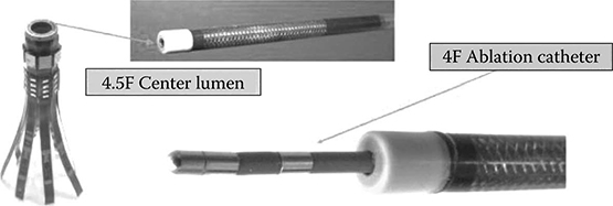
FIGURE 10.13
Real-time volumetric imaging, with a catheter-size 64-element CMUT ring array. (From Moini et al., IEEE International Ultrasonics Symposium Proceedings, 2011. Copyright IEEE with permission.)
10.5.2 large/High-Density 2D Array
Large/high-density 2D arrays are typically designed with the goal of imaging large volumes while achieving a high SNR. Current 3D ultrasound applications include facilitating ultrasound-guided biopsy, screening for breast and rectal cancer, and also prenatal imaging (Leproux et al., 2010; Maruotti et al., 2009; Natarajan et al., 2011). Currently, most of the large/high-density 2D array CMUT research is conducted in parallel with solutions that simplify the interfaces. Although the actual size of the array can vary from millimeters to centimeters, the element count can vary from 1,000 to more than 1,000,000. There are two main problems that arise from this: interfacing with a large quantity of elements and ensuring the amount of data can be processed properly such that the frame rate is still considered real time. With the CMOS process, a large number of electronic circuits can be packaged into a single chip. However, at high ultrasound frequencies where the pitch size of the phased array is less than 25 μm, the area constraint placed on the electronic circuits becomes much more difficult to meet. Assuming that the area required by the electronic circuits can be small, the cable connecting the probe to the processing system can only support a small quantity of micro-coaxial cables (typically less than 128 lines) before the cable becomes a long and stiff metal rod. As a result, some kind of simplification scheme using multiplexing or simplified phased-array algorithm is necessary. Some ongoing research techniques are briefly mentioned in the following.*
10.5.2.1 Sparse Array
This simplification technique is based on an optimization problem whereby the least amount of transducer elements is used to recreate a sound beam that can otherwise be achieved by using all the elements. Depending on the pitch, size of elements, and geometries, an acoustic field, or spatial impulse responses, can be calculated. By convoluting the responses of transmit and receive aperture, sparse array researchers can come up with different sparse patterns to tackle the optimization problem. Several sparse array patterns are shown in Figure 10.14. One obvious trade-off, however, is that with fewer elements, the SNR decreases (Lockwood and Foster, 1994).
10.5.2.2 Synthetic Array
Given that transmit and receive channels or circuitry numbers may be insufficient to support the transducer, synthetic array approaches merely break down the transmit and/or receive aperture to sub-apertures at the cost of increasing the number of pulse-echo events. An analogy can be made where multiple low-resolution images are taken to form a high-resolution image. However, this technique may not be suitable for events where the object moves at high speed (i.e., heart valves). Nonetheless, since image quality is typically of prime concern, synthetic array approach remains popular in 2D arrays (Thomenius, 1996).
* For a great comprehensive explanation of some of these techniques, please refer to “The Future of Beamforming” by K. E. Thomenius!

FIGURE 10.14
Some sparse array patters. Darker colored pixels represent transmit elements and lighter pixels represent receive elements.
10.5.2.3 Row–Column (Also Known as Crossed Electrodes)
Row–column (RC) focusing employs all elements to transmit and receive, thus maintaining a SNR comparable to that of an N by N full-matrix phased-array method. In addition, only 2N leads, pulsers, and amplifiers are used instead of N by N. This dramatically reduces the bulkiness of the system and makes the system extremely easy to implement. Also, the time it takes to complete a volumetric scan is comparable to a 1D array. These three properties address all the shortcomings associated with the sparse and synthetic array.
The RC method works by virtually rotating the aperture of an elongated 1D array between transmit and receive events. Imagine a 1D array overlaying another 1D array at an orthogonal rotation about the center. As depicted in the Figure 10.15, each transducer is connected to a column bus on the top while connected to a row bus on the bottom. At transmit mode, a column of beam is focused at each event, while at receive mode, the 2D information containing the plane intersecting the column of beam and the aperture is received (Figure 10.16). For more in-depth explanation, please refer to Logan et al. (2011).
Although there are many simplification schemes, there has not yet been a recognized “optimum” solution to tackle high-density arrays. It is likely that the electronics can physically scale down in the near future as the CMOS process continues to improve at an astonishing rate. With the general trend toward using GPU for 3D image reconstruction, the authors believe information processing or digital computation is likely not going to limit the system's quality or frame rate. Given that the speed of sound is ultimately the bottleneck that is limiting the frame rate and resolution, the authors believe that an immediate problem that requires solving lies within the development of the next generation of ultrasound cable. To ensure that high-channel count CMUT arrays can be used immediately, the development of high-density yet thin and flexible cables are needed. Otherwise, perhaps the processing unit can be so small that it can be part of the probe.
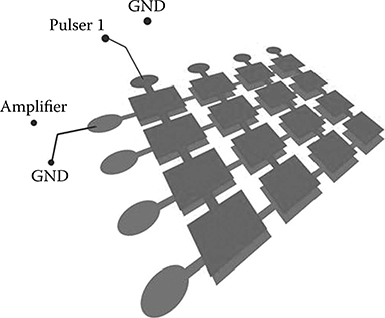
FIGURE 10.15
Row–column connection scheme. The top electrode is connected in columns, while bottom is in rows.
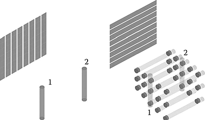
FIGURE 10.16
A single transmit column beam is formed at the transmit event. During receive event, a 2D section (dark pixels) is recorded.
10.6 Challenges
CMUT offers so many benefits over the traditional PZT transducer, yet there are several challenges that the CMUT technology needs to overcome before it can be widely adopted. The first issue is dielectric charging. When a large electric field is applied to the device, electric charges could get trapped in the insulating dielectric layer. The trapped charges create a shift in the CMUT internal electric field, causing the CMUT resonant frequency, and the resulting ultrasound frequency, to change. If different elements in a phased-array experience different frequency changes, image quality will suffer. In addition, a shift in the electric field could reduce the CMUT efficiency or cause the device to collapse. Novel CMUT structures have been proposed to mitigate the dielectric charging problem (Huang et al., 2005), but more research still needs to be done in this area.
Another limitation of the CMUT technology is the cross talk between transducer elements. Because all elements are situated on the same substrate, vibration of one element could spread to neighboring elements. The result of the cross talk is the degradation of image quality, because the unintended vibration of elements generates ultrasound that becomes noise. Models have been developed to help researchers understand the mechanism of cross talk in CMUTs (Bayram et al., 2005, 2006).
Perhaps the biggest obstacle that prevents CMUTs from achieving early success is the reliability of the CMUT device. Unlike PZT transducers that are rigid, CMUTs employ the vibration of thin membranes that can be easily damaged. Encapsulation layers have been used to protect the CMUTs, but there is always a trade-off between image quality and reliability, because while a thicker encapsulation layer provides a better protection, it reduces the efficiency of the CMUT. Fortunately, device longevity is not the biggest concern for catheter-based CMUTs because the catheter is discarded after each use. Therefore, one of the research objectives for catheter-based CMUTs is to minimize the manufacturing cost of the CMUTs and the associated front-end electronic circuits.
10.7 Conclusion
Researchers have been working on improving the CMUTs and bringing the technology to the market over the past two decades. Thanks to micromachining technologies, CMUTs offer several benefits over traditional PZT transducers such as a better axial resolution and a higher degree of integration. Because of those advantages, CMUTs are especially suitable to be used to construct small arrays in catheters or endoscopes or in high-density 2D array applications. Recent research, for example, the CMUT-integrated catheter, has demonstrated novel CMUT systems that can overcome some of the limitations of traditional medical ultrasound imaging. The capability of CMUTs can be further improved by combining high-density 2D arrays with different phased-array algorithms.
The first commercialized CMUT probe is already available, and several CMUT prototypes have been reported. Even though the CMUT technology still faces some challenges, they are tremendously outweighed by its benefits. CMUTs will unlikely replace conventional PZT transducers, but the new medical applications make them impossible to ignore. CMUTs are here to stay!
References
Bayram, B., M. Kupnik, G.G. Yaralioglu, O. Oralkan, D. Lin, X. Zhuang, A.S. Ergun, A.F. Sarioglu, S.H. Wong, and B.T. Khuri-Yakub, Characterization of cross-coupling in capacitive micromachined ultrasonic transducers. In IEEE International Ultrasonics Symposium, 1(2005): 601–604. doi:10.1109/ULTSYM.2005.1602924.
Bayram, B., G.G. Yaralioglu, M. Kupnik, and B.T. Khuri-Yakub, 5F-4 acoustic crosstalk reduction method for CMUT arrays. Proceedings in International IEEE Ultrasonics Symposium, (2006): 590–593.
Cheng, X., D.F. Lemmerhirt, O.D. Kripfgans, M. Zhang, C. Yang, C.A. Rich, and J.B. Fowlkes, CMUT-in-CMOS ultrasonic transducer arrays with on-chip electronics. In Solid-State Sensors, Actuators and Microsystems Conference, (2009): 1222–1225. doi:10.1109/SENSOR.2009.5285878.
Choe, J.W., O. Oralkan, A. Nikoozadeh, M. Gencel, D.N. Stephens, M. O'Donnell, D.J. Sahn, and B.T. Khuri-Yakub, Volumetric real-time imaging using a CMUT ring array. IEEE Transactions on Ultrasonics, Ferroelectrics and Frequency Control, 59(2012): 1201–1211.
Degertekin, F.L., R.O. Guldiken, and M. Karaman, Annular-ring CMUT arrays for forward-looking IVUS: Transducer characterization and imaging. IEEE Transactions on Ultrasonics, Ferroelectrics and Frequency Control, 53(2006): 474–482.
Gurun, G., P. Hasler, and F.L. Degertekin, Front-end receiver electronics for high-frequency monolithic CMUT-on-CMOS imaging arrays. IEEE Transactions on Ultrasonics, Ferroelectrics and Frequency Control, 58(2011): 1658–1668.
Haller, M.I. and B.T. Khuri-Yakub, A surface micromachined electrostatic ultrasonic air transducer, Proceedings in IEEE International Ultrasonics Symposium, 2(1994): 1241–1244.
Hitachi Medical Corporation, Development of ultrasonic transducer ‘Mappie’ with cMUT technology, 2009, http://www.hitachi-medical.co.jp/tech/medix/pdf/vol51/P31–34.pdf (accessed on May 21, 2013).
Huang, Y., A.S. Ergun, E. Haeggstrom, and B.T. Khuri-Yakub, New fabrication process for capacitive Micromachined ultrasonic transducers. In IEEE the Sixteenth Annual International Conference on Micro Electro Mechanical Systems, (2003): 522–525. doi:10.1109/MEMSYS.2003.1189801.
Huang, Y., E.O. Haeggström, X. Zhuang, A.S. Ergun, and B.T. Khuri-Yakub, A solution to the charging problems in capacitive micromachined ultrasonic transducers. IEEE Transactions on Ultrasonics, Ferroelectrics, and Frequency Control, 52(2005): 578–580.
Jin, X.C., I. Ladabaum, and B.T. Khuri-Yakub, Surface micromachined capacitive ultrasonic immersion transducers. Proceedings in the Eleventh Annual International Workshop on Micro Electro Mechanical Systems, (1998): 649–654.
Leproux, A., M. Van Beek, U. De Vries, M. Wasser, L. Bakker, O. Cuisenaire, M. Van Der Mark, and R. Entrekin, Automated 3D whole-breast ultrasound imaging: Results of a clinical pilot study. In SPIE Medical Imaging, (2010): 762902–762902.
Lin, D.-S., Interface engineering of capacitive micromachined ultrasonic transducers for medical applications, Doctoral Dissertation, Stanford University, (2011): 54–68.
Lockwood, G.R. and F.S. Foster, Optimizing sparse two-dimensional transducer arrays using an effective aperture approach. Proceedings in IEEE International Ultrasonics Symposium, 3(1994): 1497–1501.
Logan, A.S., L.L.P. Wong, A.I.H. Chen, and J.T.W. Yeow, A 32 × 32 element row-column addressed capacitive micromachined ultrasonic transducer. IEEE Transactions on Ultrasonics, Ferroelectrics and Frequency Control, 58(2011): 1266–1271.
Logan, A. and J.T.W. Yeow, Fabricating capacitive micromachined ultrasonic transducers with a novel silicon-nitride-based wafer bonding process. IEEE Transactions on Ultrasonics, Ferroelectrics and Frequency Control, 56(2009): 1074–1084.
Maruotti, G.M., D. Paladini, R. Napolitano, L.L. Mazzarelli, T. Russo, M. Quarantelli, M.R.D.’ Armiento, and P. Martinelli, Prenatal 2D and 3D ultrasound diagnosis of diprosopus: Case report with post-mortem magnetic resonance images (MRI) and review of the literature. Prenatal Diagnosis, 29(2009): 992–994.
Mills, D.M. and L.S. Smith, Real-time in-vivo imaging with capacitive micromachined ultrasound transducer (cMUT) linear arrays. Proceedings in IEEE International Ultrasonics Symposium, 1(2003): 568–571.
Moini , Volumetric intracardiac imaging using a fully integrated CMUT ring array: Recent developments, IEEE International Ultrasonics Symposium Proceedings, Orlando, FL, 18–21(2011): 692–695.
Natarajan, S., L.S. Marks, D.J.A. Margolis, J. Huang, M.L. Macairan, P. Lieu, and A. Fenster, Clinical application of a 3D ultrasound-guided prostate biopsy system. In Urologic Oncology: Seminars and Original Investigations, 29(2011): 334–342.
Nikoozadeh, A. , Forward-looking intracardiac imaging catheters using fully integrated CMUT arrays, IEEE International Ultrasonics Symposium Proceedings, San Diego, CA, (2010): 770–773.
Noble, R.A., R.R. Davies, M.M. Day, L. Koker, D.O. King, K.M. Brunson, and A.R.D. Jones, Cost-effective and manufacturable route to the fabrication of high-density 2D micromachined ultrasonic transducer arrays and (CMOS) signal conditioning electronics on the same silicon substrate. Proceedings in IEEE International Ultrasonics Symposium, 2(2001): 941–944. doi:10.1109/ULTSYM.2001.991874.
Stephens, D.N., U.T. Truong, A. Nikoozadeh, O. Oralkan, C. HyungSeo, J. Cannata, A. Dentinger , First in vivo use of a capacitive micromachined ultrasound transducer array-based imaging and ablation catheter. Journal of Ultrasound in Medicine: Official Journal of the American Institute of Ultrasound in Medicine, 31(2012): 247–256.
Szabo, T., Diagnostic Ultrasound Imaging: Inside Out: Inside Out. Academic Press, 2004.
Thomenius, K.E., Evolution of ultrasound beamformers. Proceedings in International Ultrasonics Symposium, 2(1996): 1615–1622.