
Chapter 2
Development of the Ideal Op Amp Equations∗
Abstract
Op Amp circuits are designed using simple electronics rules that the designer must be familiar with. It is a device that depends on the use of negative feedback to operate. Many circuits can be designed using the ideal op amp model, but the real world will affect the results. The simplest circuits are inverting and noninverting gain, adders, and differential, although more complex feedback networks are not only possible but commonplace.
Keywords
Adder circuit; Differential circuit; Ideal op amp; Inverting gain circuit; Noninverting gain circuit
2.1. Introduction
This chapter will delve into the first practical applications for the op amp. Before we delve into these applications, we will deal with the op amp in its simplest possible configuration—as a perfect or ideal component.
So what is an op amp, anyway? You have read the story of the genesis of the part, but for those of you who skipped the first chapter, I will present a shortened version in a bit more practical way.
An op amp is, first and foremost, an amplifier; hence the “amp” suffix. The “op” or “operational” part is a nod to its origins as a component in analog computers, now the “operational” part of the name probably means to most designers that it can do many things from gain to filtering to buffering. The closest many engineers will ever get to the analog computer origins are the “adder” and “subtractor” presented in this chapter.
Every inexperienced hobbyist begins with the op amp used as an amplifier as shown in Fig. 2.1.
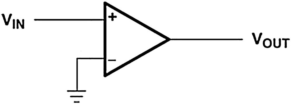
Even if you have never done this, I encourage you to try it once, to illustrate the problems Harry Black encountered in Chapter 1. Ignore the “−” (negative feedback) input by tying it off to ground. What you are left with is an amplifier with fixed gain in the thousands, perhaps as much as a million. Connected to a microphone in an ultraquiet environment, it might detect speech or other sounds from a great distance. Of course, any noise you generate or any ambient noise will swamp the amplifier and make it saturate and clip. But much more likely, it will oscillate or howl like an army of tomcats fighting in an alley, which is precisely the type of problems Harry Black encountered with his telephone line amplifiers in Chapter 1—at least the clipping part! Give Chapter 1 a read if you have not, it is fascinating!
Harry Black's solution was to essentially take advantage of that negative feedback (“−” input) to cancel most of the signal amplitude. You have all that gain, and promptly throw away the vast majority of it by feeding the amplified output back 180 degrees out of phase, canceling most of the signal. You use the voltage divider described in Appendix A to determine how much of that signal is canceled, and—presto—you have just started using the noninverting op amp configuration of 2.3! But before we delve into that, or other useful op amp circuits, we need to take a baby step. We need to introduce the parameters that define an op amp. And the perfect beginning point is the perfect—or ideal—op amp. Real-world op amp parameters, and their effect on circuit configurations, will be covered in subsequent chapters and Appendix B when the elementary analysis is complete.
2.2. Ideal Op Amp Assumptions
The name ideal op amp is applied to this and similar analysis because the salient parameters of the op amp are assumed to be perfect. This assumption simplifies the analysis, thus it clears the path for insight. It is so much easier to see the forest when the underbrush is cleared away. Although the ideal op amp analysis makes use of perfect parameters, the analysis is often valid because some op amps approach perfection. In addition, when working at low frequencies, several kilohertz, the ideal op amp analysis produces accurate answers. Voltage feedback op amps are covered in this chapter, and current feedback op amps are covered in a later chapter.
An engineer may wish that an ideal op amp existed at times, but if such a component actually did exist, it would destroy the known universe! See the end of this chapter for an explanation. Thankfully, there is no such thing as an ideal op amp, but present day op amps come so close to ideal that ideal op amp analysis approaches actual analysis. Op amps depart from the ideal in the following ways:
• The ideal assumes that input offset voltage is zero. DC parameters, such as input offset voltage, cause departure from the ideal.
• Assume that the current flow into the input leads of the op amp is zero. This assumption is almost true in FET op amps where input currents can be less than a picoampere, but this is not always true in bipolar high-speed op amps where tens of microamperes input currents are found.
• The op amp gain is assumed to be infinite, hence it drives the output voltage to any value to satisfy the input conditions. This assumes that the op amp output voltage can achieve any value. In reality, saturation occurs when the output voltage comes close to a power supply rail, but reality does not negate the assumption, it only bounds it.
• The gain drives the output voltage, until the voltage between the input leads (the error voltage) is zero, therefore the voltage between the input leads is zero. The implication of zero voltage between the input leads means that if one input is tied to a hard voltage source such as ground, then the other input is at the same potential.
• The current flow into the input leads is zero, so the input impedance of the op amp is infinite.
• The output impedance of the ideal op amp is zero. The ideal op amp can drive any load without an output impedance dropping voltage across it. The output impedance of most op amps is a fraction of an ohm for low current flows, so this assumption is valid in most cases.
• The frequency response of the ideal op amp is flat; this means that the gain does not vary as frequency increases. By constraining the use of the op amp to the low frequencies, we make the frequency response assumption true.
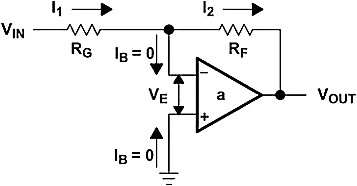
2.3. The Noninverting Op Amp
The noninverting op amp has the input signal connected to its noninverting input (Fig. 2.3), thus its input source sees infinite impedance. There is no input offset voltage because VOS = VE = 0, hence the negative input must be at the same voltage as the positive input. The op amp output drives current into RF until the negative input is at the voltage, VIN. This action causes VIN to appear across RG.


The voltage divider rule is used to calculate VIN; VOUT is the input to the voltage divider, and VIN is the output of the voltage divider. Since no current can flow into either op amp lead, use of the voltage divider rule is allowed. Eq. (2.1) is written with the aid of the voltage divider rule, and algebraic manipulation yields Eq. (2.2) in the form of a gain parameter.
Under these conditions VOUT = 1 and the circuit becomes a unity gain buffer. RG is usually deleted to achieve the same results, and when RG is deleted, RF can be made into a short (op amp output is connected to its inverting input with a wire). Some op amps are self-destructive when RF is a short (particularly current feedback amplifiers), so RF is used in many buffer designs. When RF is included in a buffer circuit, its function is to protect the inverting input from an overvoltage to limit the current through the input electrostatic discharge structure (typically < 1 mA), and it can have almost any value.
2.4. The Inverting Op Amp
The noninverting input of the op amp circuit is grounded. The assumption is made that the input error voltage is zero, so the feedback keeps inverting the input of the op amp at a virtual ground (not actual ground but acting like ground). The current flow in the input leads is assumed to be zero, hence the current flowing through RG equals the current flowing through RF (Fig. 2.4). Using Kirchhoff's law, we write Eq. (2.4); and the minus sign is inserted because this is the inverting input. Algebraic manipulation gives Eq. (2.5).
Notice that the gain is only a function of the feedback and gain resistors, so the feedback has accomplished its function of making the gain independent of the op amp parameters. The actual resistor values are determined by the impedance levels that the designer wants to establish. If RF = 10 k and RG = 10 k the gain is −1 as shown in Eq. (2.5), and if RF = 100 k and RG = 100 k the gain is still −1. The impedance levels of 10 or 100 k determine the current drain, the effect of stray capacitance, and a few other points. The impedance level does not set the gain; the ratio of RF/RG does.
One final note; the output signal is the input signal amplified and inverted. The circuit input impedance is set by RG because the inverting input is held at a virtual ground.
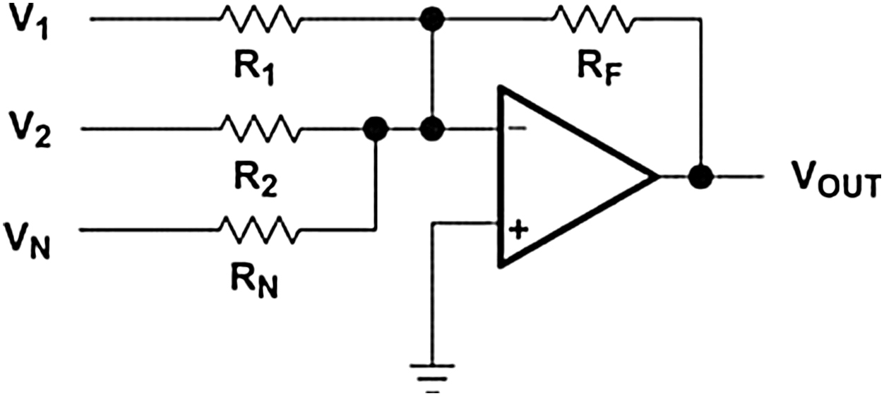
2.5. The Adder
An adder circuit can be made by connecting more inputs to the inverting op amp (Fig. 2.5). The opposite end of the resistor connected to the inverting input is held at virtual ground by the feedback; therefore, adding new inputs does not affect the response of the existing inputs.
Superposition is used to calculate the output voltages resulting from each input, and the output voltages are added algebraically to obtain the total output voltage. Eq. (2.6) is the output equation when V1 and V2 are grounded. Eqs. (2.7) and (2.8) are the other superposition equations, and the final result is given in Eq. (2.9).
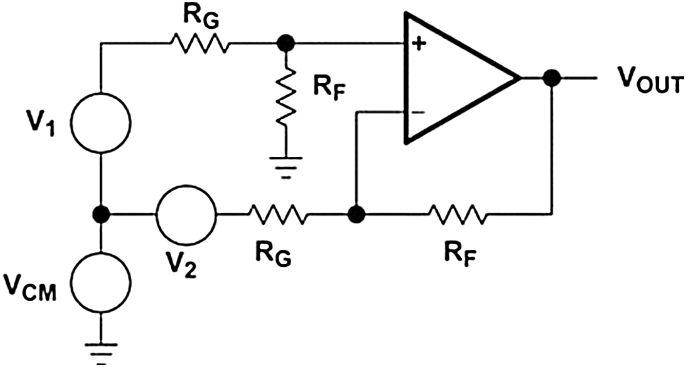
2.6. The Differential Amplifier
The differential amplifier circuit amplifies the difference between signals applied to the inputs (Fig. 2.6). Superposition is used to calculate the output voltage resulting from each input voltage, and then the two output voltages are added to arrive at the final output voltage.
The op amp input voltage resulting from the input source, V1, is calculated in Eqs. (2.10) and (2.11). The voltage divider rule is used to calculate the voltage, V+, and the noninverting gain equation (Eq. 2.2) is used to calculate the noninverting output voltage, VOUT1.

The inverting gain equation (Eq. 2.5) is used to calculate the stage gain for VOUT2 in Eq. (2.12). These inverting and noninverting gains are added in Eq. (2.13).
Next, to simplify the equation, R1 is made equal to R3, and R2 made equal to R4:
It is now obvious that the differential signal (V1 − V2) is multiplied by the stage gain, so the name differential amplifier suits the circuit. Because it only amplifies the differential portion of the input signal, it rejects the common-mode portion of the input signal. A common-mode signal is illustrated in Fig. 2.7. Because the differential amplifier strips off or rejects the common-mode signal, this circuit configuration is often employed to strip DC or injected common-mode noise off a signal.
The disadvantage of this circuit is that the two input impedances cannot be matched when it functions as a differential amplifier, thus there are two and three op amp versions of this circuit specially designed for high-performance applications requiring matched input impedances.
2.7. Complex Feedback Networks
When complex networks are put into the feedback loop, the circuits get harder to analyze because the simple gain equations cannot be used. The usual technique is to write and solve node or loop equations. There is only one input voltage, so superposition is not of any use, but Thevenin's theorem can be used as is shown in the example problem given below.
Sometimes it is desirable to have a low-resistance path to ground in the feedback loop. Standard inverting op amps cannot do this when the driving circuit sets the input resistor value, and the gain specification sets the feedback resistor value. Inserting a T network in the feedback loop (Fig. 2.8) yields a degree of freedom that enables both specifications to be met with a low DC resistance path in the feedback loop.
Break the circuit at point X–Y, stand on the terminals looking into R4, and calculate the Thevenin equivalent voltage as shown in Eq. (2.15). The Thevenin equivalent impedance is calculated in Eq. (2.16).


Replace the output circuit with the Thevenin equivalent circuit as shown in Fig. 2.9, and calculate the gain with the aid of the inverting gain equation as shown in Eq. (2.17).
Substituting the Thevenin equivalents into Eq. (2.17) yields Eq. (2.18).
Algebraic manipulation yields Eq. (2.19).
 (2.19)
Specifications for the circuit you are required to build are an inverting amplifier with an input resistance of 10 k (RG = 10 k), a gain of 100, and a feedback resistance of 20 K or less. The inverting op amp circuit cannot meet these specifications because RF must equal 1000 k. Inserting a T network with R2 = R4 = 10 k and R3 = 485 k approximately meets the specifications.
2.8. Impedance Matching Amplifiers
High-frequency op amp circuits may use coaxial cable to transmit and receive signals. The cable connecting these circuits has a characteristic impedance of 50 Ω. To prevent reflections, which cause distortion and ghosting, the input and output circuit impedances must match the 50 Ω cable.
Matching the input impedance is simple for a noninverting amplifier because its input impedance is very high; just make RIN = 50 Ω. RF and RG can be selected as high values, in the hundreds of ohms range, so that they have minimal affect on the impedance of the input or output circuit. A matching resistor, RM, is placed in series with the op amp output to raise its output impedance to 50 Ω; a terminating resistor, RT, is placed at the input of the next stage to match the cable (Fig. 2.10).
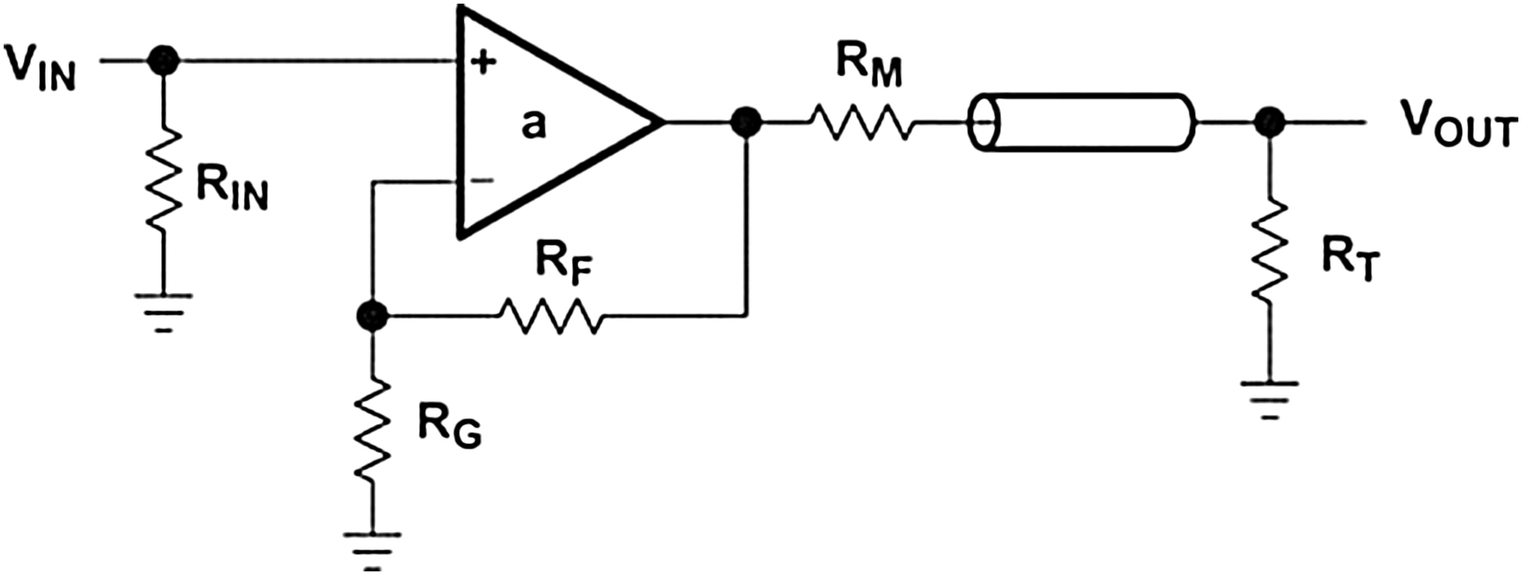
The matching and terminating resistors are equal in value, and they form a voltage divider of 1/2 because RT is not loaded. Very often RF is selected equal to RG so that the op amp gain equals 2. Then the system gain, which is the op amp gain multiplied by the divider gain, is equal to 1 (2 × 1/2 = 1).
2.9. Capacitors
Capacitors are a key component in a circuit designer's tool kit, thus a short discussion on evaluating their effect on circuit performance is in order. Capacitors have an impedance of XC = 1/2πfC. Note that when the frequency is zero, the capacitive impedance (also known as reactance) is infinite, and that when the frequency is infinite the capacitive impedance is zero. These end points are derived from the final value theorem, and they are used to get a rough idea of the effect of a capacitor. When a capacitor is used with a resistor, they form what is called a break point. Without going into complicated math, just accept that the break frequency occurs at f = 1/(2πRC), and the gain is −3 dB at the break frequency.
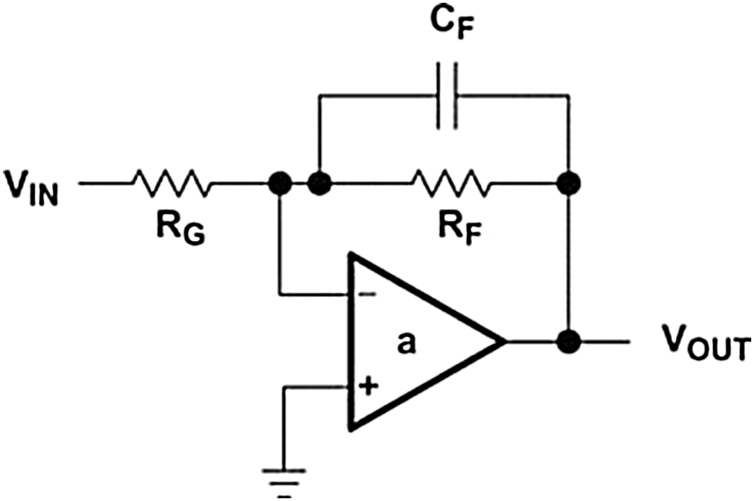
The low-pass filter circuit shown in Fig. 2.11 has a capacitor in parallel with the feedback resistor. The gain for the low-pass filter is given in Eq. (2.20).
At very low frequencies XC ⇒ ∞, so RF dominates the parallel combination in Eq. (2.20), and the capacitor has no effect. The gain at low frequencies is −RF/RG. At very high frequencies XC ⇒ 0, so the feedback resistor is shorted out, thus reducing the circuit gain to zero. At the frequency where XC = RF the gain is reduced by  because complex impedances in parallel equal half the vector sum of both impedances.

Connecting the capacitor in parallel with RG where it has the opposite effect makes a high-pass filter (Fig. 2.12). Eq. (2.21) gives the equation for the high-pass filter.
At very low frequencies XC ⇒ ∞, so RG dominates the parallel combination in Eq. (2.21), and the capacitor has no effect. The gain at low frequencies is 1 + RF/RG. At very high frequencies XC ⇒ 0, so the gain setting resistor is shorted out thus increasing the circuit gain to maximum.
This simple technique is used to predict the form of a circuit transfer function rapidly. Better analysis techniques are presented in later chapters for those applications requiring more precision.
2.10. Why an Ideal Op Amp Would Destroy the Known Universe
I moved this somewhat humorous explanation to later in the chapter so as not to distract from the important discussions of circuit configuration above. This section provides an excellent review of ideal op amp parameters, in a way you can remember them in chapters to come. An ideal op amp has the following specifications:
• It draws no supply current, therefore has no power supplies. Therefore, it does not even have to be turned on to be dangerous!
• It has no VOH and VOL limitations because it has no power supplies. Therefore, its output voltage swings from ±∞ Volts.
• It has zero output resistance, and therefore it is capable of supplying infinite current at each voltage extreme.
• It has infinite open-loop gain; therefore the slightest input signal would allow it to swing to ± infinite voltage (that is, without feedback components).
• It has infinite slew rate, and therefore would swing to either rail—both equally destructive—instantly.
Therefore an ideal op amp, just lying on the table with no power applied, would instantly take a quantum difference between its + and − terminals and amplify it to an infinite voltage output at infinite current. The resulting surge of power would be a sphere of destruction radiating out from the op amp at the speed of light!
This somewhat humorous analysis is included to drive home a few points:
1. If the ideal op amp model is employed, the engineer must also know how real-world op amp parameters degrade and alter the ideal op amp model. An ideal op amp model is a useful tool for initial phases of simulation and analysis, but does not adequately explain real-world op amp behavior.
2. All of the mathematical analysis above can be boiled down to a simple concept: The op amp will do whatever it has to do at its output to equalize the voltages at its inputs. This is the entire content of this book, distilled down to its simplest form. This fundamental concept can be used to derive all of the behavior of all op amp circuits in all applications. Of course, it must be filtered through statement (1) for real-world op amps.
3. A very astute analog design engineer might see one fallacy in this “death star” scenario: “Where is the return path?” When a single-ended op amp is employed, the return path is to ground. But when no power supplies are utilized, there is no ground! So to be technically correct, the only type of ideal op amp that would destroy the known universe is a fully differential type, where the return for one output is the other output. This book will explain in detail the subject of proper return to ground for single-ended op amps and for single-ended op amps configured in single-supply operation.
2.11. Summary
When the proper assumptions are made, the analysis of op amp circuits is straightforward. These assumptions, which include zero input current, zero input offset voltage, and infinite gain, are realistic assumptions because the new op amps make them essentially true in most real-world applications.
When the signal is comprised of low frequencies, the gain assumption is valid because op amps have very high gain at low frequencies. When CMOS op amps are used, the input current is in the femtoamp range; close enough to zero for most applications. Laser-trimmed input circuits reduce the input offset voltage to a few microvolts; close enough to zero for most applications. The ideal op amp is becoming real; especially for undemanding applications.
..................Content has been hidden....................
You can't read the all page of ebook, please click here login for view all page.