
Chapter 19
Using Op Amps for RF Design
Abstract
Op amps have become fast enough that they can now be considered for RF designs, traditionally the domain of discrete transistors. There are many parameters for RF circuit design that are different from those specified with op amps. They are, however, related in ways that are explained. Real sample RF circuits are presented.
Keywords
−1 dB compression point; Current-feedback amplifier; Noise figure; Peaking; Phase linearity; Stage gain; Termination; Voltage-feedback amplifier
19.1. Introduction
RF design used to be the exclusive domain of discrete devices. The advent of new generations of high-speed voltage- and current-feedback op amps has made it possible to use op amps for RF design. Op amp–based RF circuitry is easier to design and has less risk associated. “Tweaking” in the lab can be almost eliminated. Although there are many advantages to using op amps, traditional RF designers are reluctant to utilize them. They are confronted with a bewildering array of op amp parameters, many of which do not relate directly to the set of design parameters they are familiar with. This chapter bridges the gap between RF designers and op amp designers, giving the RF designer common ground with which to begin their design.
19.2. Voltage Feedback or Current Feedback?
The RF designer that is considering op amps is presented with a dilemma—are voltage-feedback amplifiers or current-feedback amplifiers better for the design? Frequency of operation is usually the most demanding aspect of RF design, and this makes the op amp bandwidth a critical parameter. The bandwidth specification given in op amp data sheets only refers to the point where the unity gain bandwidth of the device has been reduced by 3 dB by internal compensation and/or parasitics—which is not very useful for determining the actual operating frequency range of the device in an RF application.
Internally compensated voltage-feedback amplifier bandwidth is dominated by an internal “dominant-pole” compensation capacitor. This gives them a constant gain/bandwidth limitation. Current-feedback amplifiers, in contrast, have no dominant-pole capacitor, and therefore can operate much closer to their maximum frequency at higher gain. Stated another way, the gain/bandwidth dependence has been broken but not to the degree most designers would want. In practice, current-feedback op amps offer only a slight advantage over voltage-feedback op amps.
19.3. RF Amplifier Topology
The traditional RF amplifier shown in Fig. 19.1 uses a transistor (or in early days a tube) as the gain element. DC bias (+Vbb) is injected into the gain element at the load through a bias resistor Rb. RF is blocked from being shorted to the supply by an inductor Lc, and DC is blocked from the load by a coupling capacitor.
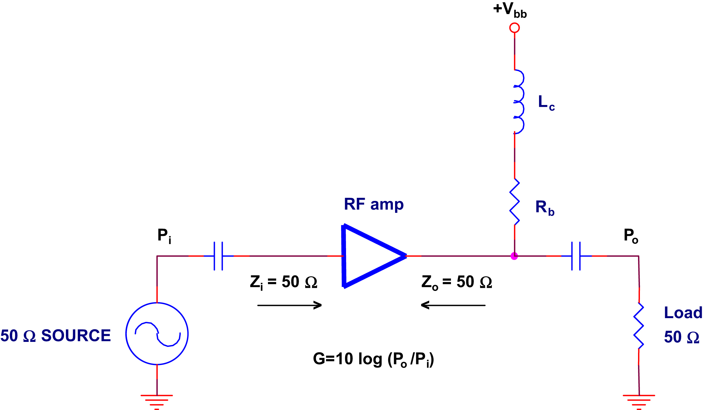
Both the input impedance and the load are 50 Ω, which ensures matching between stages.
When an op amp is substituted as the active circuit element, several changes are made to accommodate it.
By themselves, op amps are differential input, open-loop devices. They are intended to be operated in a closed-loop topology (different from a receiver's AGC (automatic gain control) loop). The feedback loop for each op amp must be closed locally, within the individual RF stage.
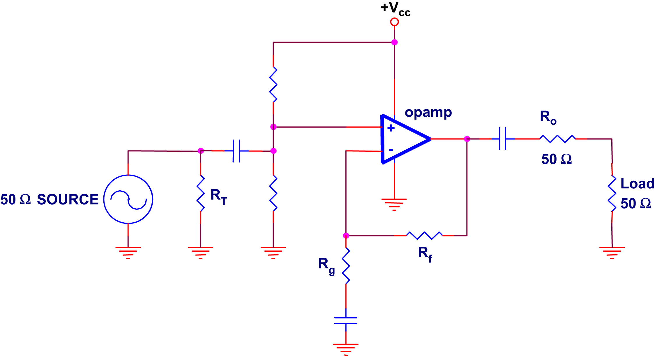
There are two ways close to an op amp locally: inverting and noninverting. These terms refer to whether the output of the op amp circuit is inverted from the input or not. From the standpoint of RF design, this is seldom of any concern. For all practical purposes, either configuration will work and give equivalent results, but RF designers may find the noninverting configuration of Fig. 19.2 easier to work with, because the gain setting elements are not part of impedance matching.
The input impedance of the noninverting input is high, so the input is terminated with a 50 Ω resistor. Gain is set by the ratio of RF and RG:
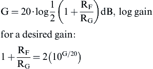
The gain of this stage as shown should never be below ½ (−6 dB), because most op amps are unity gain stable.
The output of the stage is converted to 50 Ω by placing a 50 Ω resistor in series with the output. This combined with a 50 Ω load, means that the gain is divided by 2 (−6 dB) in a voltage divider. A unity gain (0 dB) gain stage would become a gain of ½, or −6 dB.
A virtual ground is generated on the noninverting input after the coupling capacitor, to raise the operating point of the op amp to a virtual ground halfway between the supply voltage and ground.
Coupling capacitors are needed to isolate preceding and succeeding stages, and the gain resistor RG from the virtual ground DC potential. These two resistors—see in Fig. 19.2 to the right of the input coupling cap—should be large in relationship to RT, but small enough to satisfy the input bias requirements of the op amp. This is seldom a concern to the RF designer, values of 1–10 k are probably correct. They should be equal in value to create a voltage divider of ½ on the supply, creating the DC biasing point (DC operating point) of the stage. The blocking capacitors should be selected to have low impedance at the operating frequency, not so small that they affect the gain of the stage directly, or cause unacceptable variations in gain over the operating range of the stage.
19.4. Op Amp Parameters for RF Designers
When designing for RF, problems can arise because op amp sheets show a totally different set of parameters than are considered for RF designs. This situation has been improving over the years as more and more high-speed amplifiers have been introduced, but there are still differences. This section will go over the more important parameters and specifications and show RF designers how to interpret op amp data sheet specifications to meet their needs.
19.4.1. Stage Gain
Op amp designers think of the gain of an op amp stage in terms of voltage gain. RF designers, in contrast, are used to thinking of RF stage gain in terms of power:
The forward transmission S21 is specified over the operating frequency range of interest. S21 is never specified on an op amp data sheet because it is a function of the gain, which is set by the input and feedback resistors RF and RG. The forward transmission of a noninverting op amp stage shown in Fig. 19.2 is:
Op amp data sheets show open-loop gain and phase. It is the responsibility of the designer to know the closed-loop gain and phase. Fortunately, this is not hard to do. The data sheets many times include excellent graphs of open-loop bandwidth and most of the time include phase. Closing the loop produces a straight line across the graph at the desired gain, curving to meet the limit. The open-loop bandwidth plot should be used as an absolute maximum and should not be approached too closely.
An added benefit of using current-feedback amplifiers is that the values of RF and RG are specified in the data sheet. Please note, however, that the gains in the data sheet will not take 50 Ohm matching into account, so the stage gains will be ½ what the data sheet specifies for a given value of RF and RG.
19.4.2. Phase Linearity
Oftentimes, a designer is concerned with the phase response of an RF circuit. This is particularly the case with video design, which is a specialized type of RF design. Current-feedback amplifiers tend to have better phase linearity than voltage-feedback amplifiers:
• Voltage-feedback THS 4001: Differential phase = 0.15 degrees
• Current-feedback THS 3001: Differential phase = 0.02 degrees

19.4.3. Frequency Response Peaking
Current-feedback amplifiers allow an easy resistive trim for frequency peaking that has no impact on the forward gain. Fig. 19.3 shows this adjustment added to a noninverting circuit. This resistive trim inside the feedback loop has the effect of adjusting the loop gain, and hence the frequency response without adjusting the signal gain, which is still set by RF and RG.
Values for RF and RG must be reduced to compensate for the addition of the trim potentiometer, although their ratio and hence the gain should remain the same. The adjustment range of the pot, combined with the lower RF value ensures that the frequency response can be peaked for slight current-feedback amplifier parameter variations.
19.4.4. −1 dB Compression Point
The −1 dB compression point is defined as the output power, at a fixed input frequency, where the amplifier's actual output power is 1 dBm less than expected. Stated another way, it is the output power at which the actual amplifier gain has been reduced by 1 dB from its value at lower output powers. The −1 dB compression point is the way RF designers talk about voltage rails.
Op amp designers and RF designers have very different ways of thinking about voltage rails, which are related to the requirements of the systems that they design:
• An RF designer, on the other hand, is often concerned with squeezing the last half dB out of an RF circuit. In broadcasting, for example, a very slight increase in dBs means a lot more coverage. More coverage means more audience and more advertising dollars. Therefore, slight clipping is acceptable as long as resulting spurs are within FCC regulations.
Standard AC-coupled RF amplifiers show a relatively constant −1 dB compression power over their operating frequency range. For an operational amplifier, the maximum output power depends strongly on the input frequency. The two op amp specifications that serve a similar purpose to −1 dB compression are VOM and slew rate.
At low frequencies, increasing the power of a fixed frequency input will eventually drive the output “into the rails”—the VOM specification. Oftentimes, VOM is broken up into separate low and high clipping levels, which are specified as VOL and VOH, respectively. At high frequencies, op amps will reach a limit on how fast the output can transition (respond to a step input). This is the slew rate limitation of the amplifier. The op amp slew rate specification is divided by two, because of the matching resistor used at the output.
As is the case for op amps used in any other application, it is probably best to avoid operation near the rails, as the inevitable distortion will produce harmonics in the RF signal—harmonics that are probably undesirable for FCC testing. That said, if harmonics are still at an acceptable level at the −1 dB compression point, it can be a very useful way to boost power to a maximum level out of the circuit.
19.4.5. Noise Figure
The RF noise figure is the same thing as op amp noise, when an op amp is the active element. There is some effect from thermal noise in resistors used in RF systems, but the resistor values in RF systems are usually so small that their noise can be ignored.
Noise for an op amp RF circuit is dependent on the following:
• the bandwidth being amplified
• gain
This example assumes the  op amp. The application is a 10.7 MHz IF amplifier. The signal level is 0 dBV. The gain is unity.
Fig. 19.4 is extrapolated from real data. The 1/f corner frequency, in this case, is much lower than the bandwidth of interest. Therefore, the 1/f noise can be completely discounted (assuming that filtering removes any noise that would cause the amplifier or data converter to saturate).
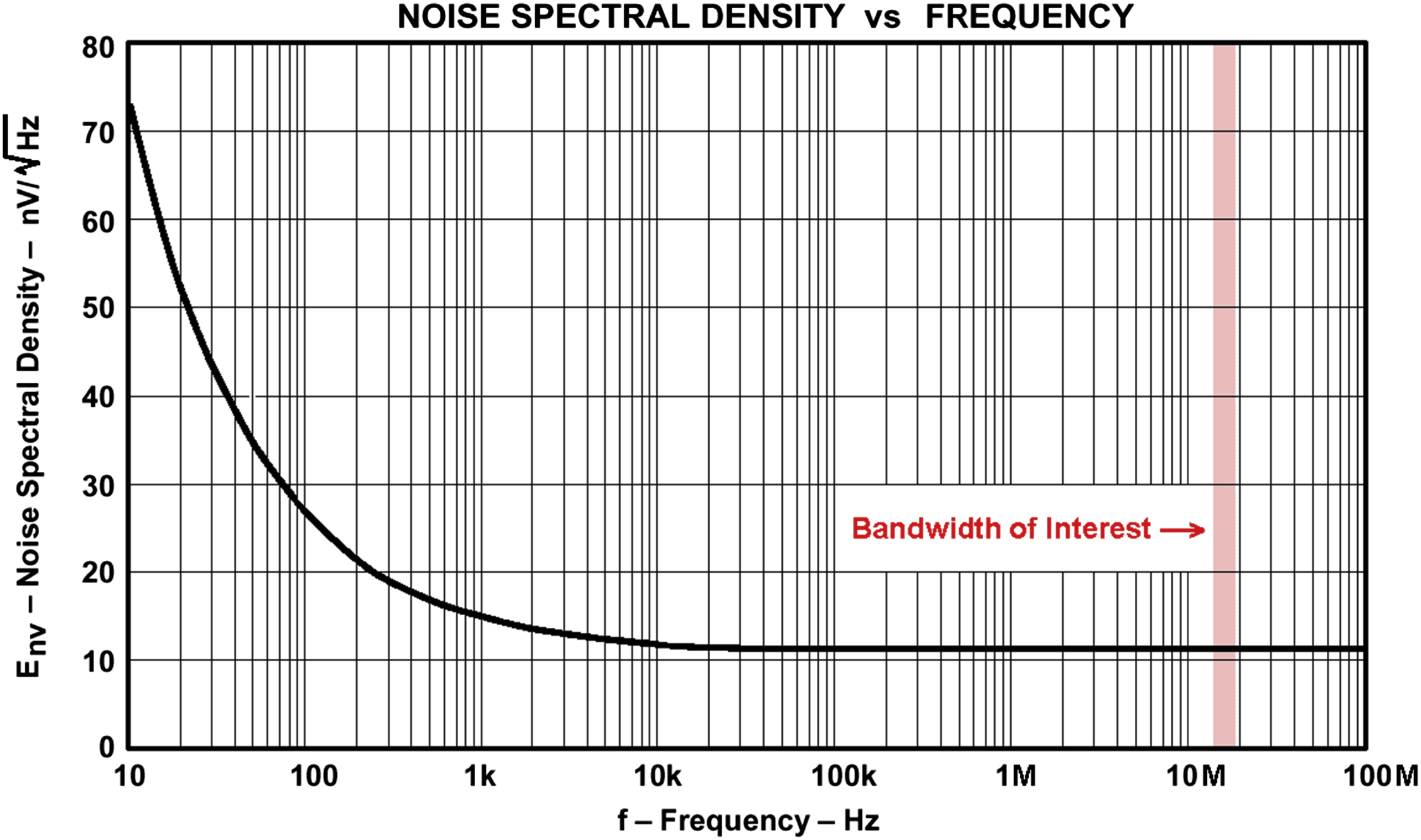
For narrow bandwidths, noise may be quite low! Various bandwidths are shown in Table 19.1.
There is an advantage to be had from reducing the bandwidth. Noise is amplified by the gain of the stage. Therefore, if a stage has high gain, care must be taken to find a low noise op amp. If the gain of a stage is lower, then the noise will not be amplified as much, and a less expensive op amp may be suitable.
19.5. Wireless Systems
Fig. 19.5 shows an example of a dual-IF cellular receiver. The receiver contains two mixer stages reminiscent of a classic double conversion superheterodyne receiver.
The RF designer wishing to use op amps for some of the gain stages needs to realize the current state of the art in op amp technology. Op amps are excellent choices for driving the analog-to-digital converter (ADC), low-pass filtering, and even second IF gain. But when you attempt to use op amps for the first IF frequency of 660 MHz in Fig. 19.5, you will quickly run out of open-loop gain. This limits the RF designer to using op amps in the final stages of that design, although unity gain buffers can be employed for impedance matching at higher frequencies. For the most part, though, op amps are not suitable for UHF applications.

19.5.1. Broadband Amplifiers
Current-feedback amplifiers are the component of choice for broadband amplifiers. The THS3202 was tested for its wide bandwidth and fast slew rate. A THS3202 evaluation board made a convenient platform on which to construct the circuits presented in here. The key questions explored just how much gain an op amp–based circuit is capable of, and over what frequency range? The circuit in Fig. 19.6 was used to explore these questions. It was first configured as a single stage, consisting of device A of a dual package, a 301 Ω feedback resistor, a 16.5 Ω gain resistor, and a 49.9 Ω back termination resistor. This configuration produces an amplifier gain of 20, a stage gain of 10 when connected to a 50 Ω monitoring device.
Note the simplicity of this circuit compared to traditional RF circuitry. Provide the op amp, termination and decoupling components, and two resistors and the circuit is done! The 301 Ω (RF) and 16.5 Ω (RG) resistors are all that are required to set the stage gain. The stage's gain can be set precisely by the resistors alone, one of the op amp–based design's strong points. This circuit produces the lower amplitude curve in Fig. 19.7.
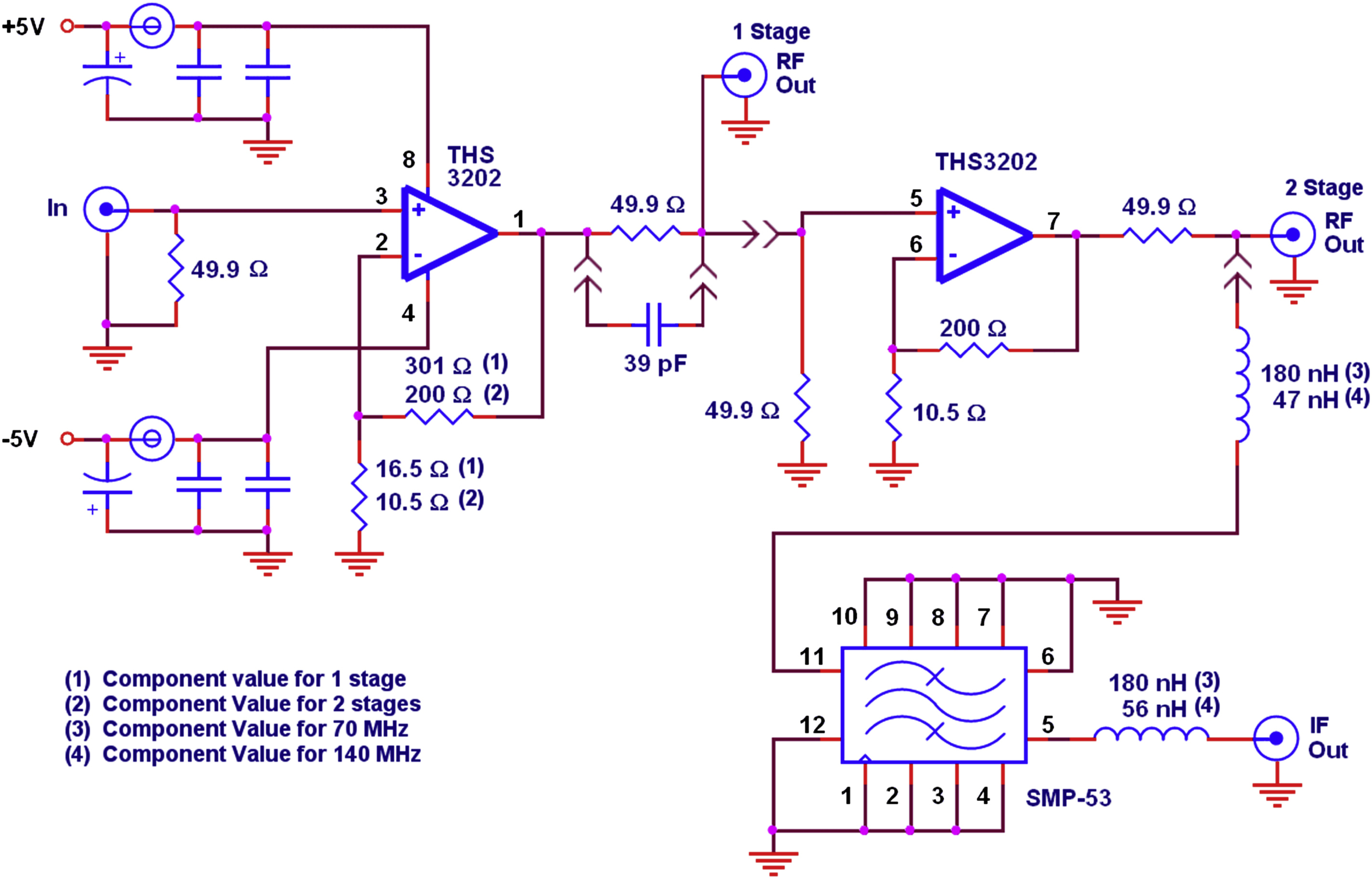
The op amp stage's voltage gain itself is 20, but this is cut in half by the back termination resistor's action in combination with the load. The RF amplifier's −3 dB point is about 390 MHz. If a flat gain over frequency is required, this circuit is only usable to about 200 MHz. Input and output voltage standing wave ratio (VSWR) values are better than 1.01:1 for most of the bandwidth, only degrading to about 1.1:1 near 200 MHz. S12 is −75 dB over most bandwidth, only degrading to −50 dB near the bandwidth limit.

One might wonder if more gain could be coaxed from the stage by lowering the gain resistor (RG) even more. The answer is yes, but there is a practical limit. Remember that the feedback resistor (RF) is a large determining factor for current-feedback amplifier stability. Remember also that RG has to drop proportionally more. One can see that it would not be long until RG's value becomes impractically small. Lab tests were attempted with various RF values. The result indicated there is no advantage to making it smaller than 200 Ω. Below that, peaking starts to occur regardless of RG's value, becoming worse and worse as the resistance is made lower and lower. This is exactly what one would expect, because one of the things a designer cannot do in working with current-feedback amplifiers is to make RF a short.
More gain requires cascading multiple stages of THS3202 op amps. Fortunately for the designer, the THS3202 is a dual device, making a two-stage RF amplifier easy to implement at very little additional cost.
To convert the amplifier to two stages, the feedback resistor is lowered to 200 Ω, and the gain resistor lowered to 10.5 Ω. A second stage is then connected to the first, using the same values for the feedback and gain resistors. Isolation is accomplished by using interstage termination resistors. The optional 39 pF capacitor provides peaking to compensate for some high-frequency roll-off. Unfortunately, it also creates capacitive load on the first amplifier output. This increases the first stage's tendency to peak as seen in the upper curve of 0. This indicates a tendency toward instability, and it manifests itself by poorer IP3 performance. If maximum IP3 performance is needed, the designer should delete the capacitor and live with less bandwidth from the stage. The other S parameters for this circuit are similar to the single op amp's case.
At this point, it is important to talk about signal levels. All of the above points in the direction of impressive performance, but if these benefits only apply to very small signals they are hardly benefits at all!
The signal level a designer can pass through an op amp is determined by its input and output voltage rails, as described by the device's data sheet. They form a set of high- and low-voltage “hard clipping” points for the signal as it passes through the operational amplifier. Consequently, the −1 dB compression point occurs very soon after any voltage rail limitation has been breached. The wise designer will not attempt to squeeze that last dB from the stage because the hard clipping points may produce substantial harmonics.
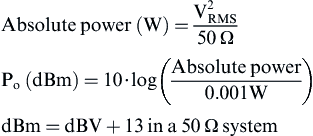
For a THS3202 stage, the amplifier's output can swing ±3.2 V, therefore the output of the stage can swing ±1.6 V. This corresponds to 14 dBm of output power.
19.5.2. IF Amplifiers
The gain circuit shown in Fig. 19.6 can be cascaded with SAW (surface acoustic wave) filters to form high-performance IF stages. The only design consideration is the insertion loss of the filter, which may not be a constant value from part to part, or from batch of parts to batch of parts. If precise gain is needed from the stage, the designer may need to include a trim resistor in one or both stages. This trim adjustment, however, will not affect the stage's tuning except for a slight effect on its upper frequency limit.
It is easy to cascade the dual wideband RF amplifier with SAW filters. Sawtek conveniently provided an EVM board, which greatly simplified prototyping. All that was required was to provide a short SMA to SMA cable between the two boards. It is important to place the SAW filter element after the gain stage, so noise generated in the op amp circuitry is filtered with the same response as the signal. If the gain stage were placed after the SAW filter, the amplifier stage's broadband noise response would be passed to the next stage instead of a filtered, narrow-band response.
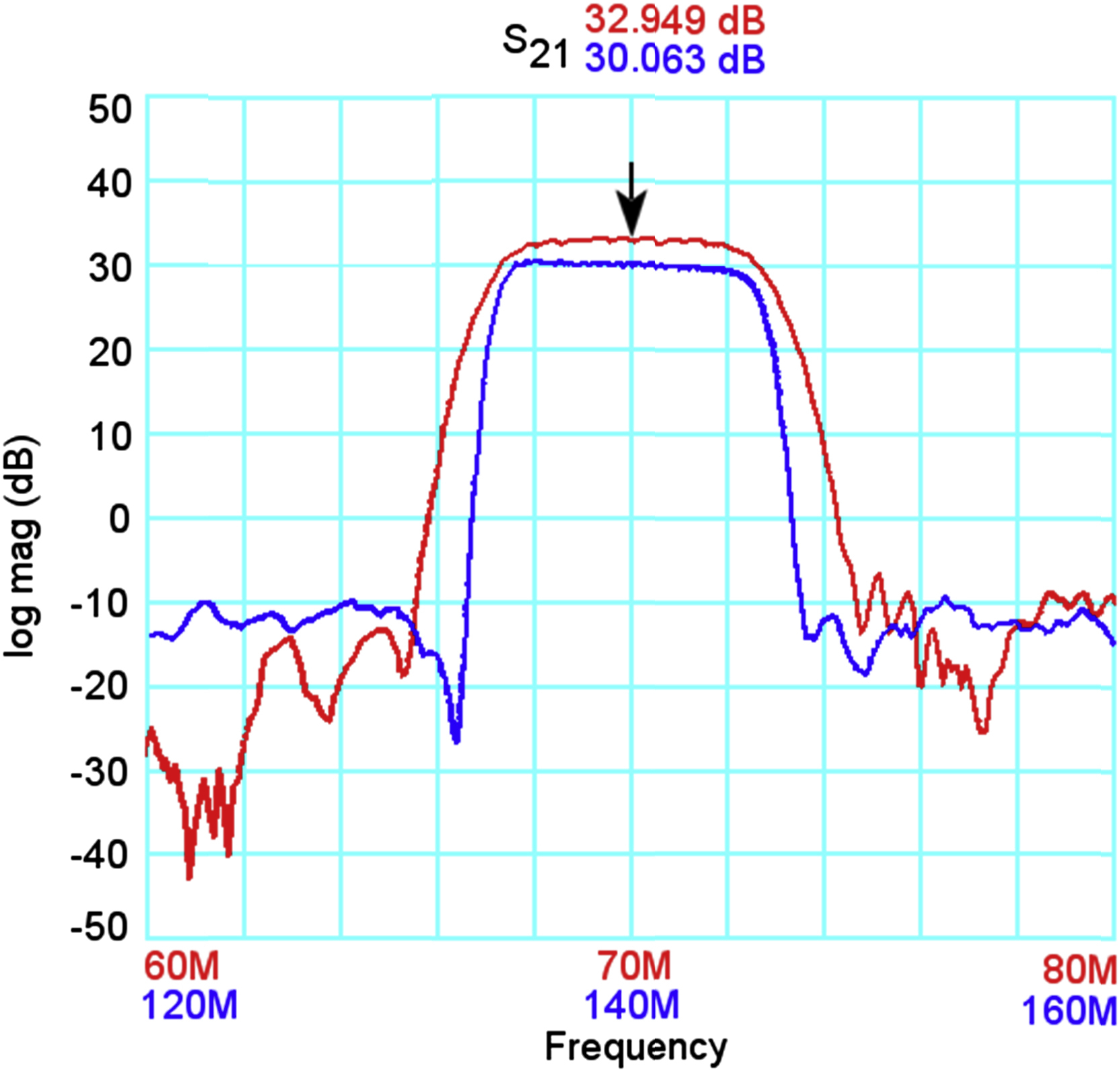
The IF amplifiers of 70 and 140 MHz find use in cellular telephone base stations and satellite communications receivers. A Sawtek 854660 filter was selected for 70 MHz, and a Sawtek 854916 filter was selected for 140 MHz. These filters require input and output inductors and operate with standard 50 Ω input and output. A 70 MHz SAW filter produces the upper response curve, and the 140 MHz filter produces the lower response curve shown in Fig. 19.8:
The most outstanding response curves featured in Fig. 19.8: IF amplifier response is that they are almost identical in shape to the filter curves provided by Sawtek. Narrow-band response is shown in 0, but there is virtually no harmonic content when the broadband response is examined. In other words, the amplifier is providing gain while not adding undesirable harmonic content. The insertion loss of the 70 MHz SAW filter is about 7 dB. The insertion loss of the 140 MHz SAW filter is only 8 dB, but the gain circuit itself is starting to roll off at this frequency, accounting for the rest of the loss. Careful examination of the lower pass-band shows the slight roll-off due to the broadband stage characteristic.
19.6. High-Speed Analog Input Drive Circuits
Communication ADCs, for the most part, have differential inputs and require differential input signals to properly drive the device. Drive circuits are implemented with either RF transformers or high-speed differential amplifiers with large bandwidth, fast settling time, low output impedance, good output drive capabilities, and a slew rate of the order of 1500 V/μS. The differential amplifier is usually configured for a gain of one or two and is used primarily for buffering and converting the single-ended incoming analog signal to differential outputs. Unwanted common-mode signals, such as hum, noise, DC, and harmonic voltages are generally attenuated or canceled out. Gain is restricted to wanted differential signals, which is often 1–2 V.
The analog input drive circuit, as shown in Fig. 19.9, employs a THS4141 device. This device offers fast speed, linear operation over a wide frequency range, and wide power-supply voltage range, but draws slightly more current than a BiCMOS device. The −3 dB bandwidth is 120 MHz measured at the output of the amplifier. The analog input VIN is AC-coupled to the THS4141 and the DC voltage Vocm is the applied input common-mode voltage. The combination R47–C57 and R26–C34 are selected to meet the desired frequency roll-off. If the input signal frequency is above 5 MHz, higher-order low-pass filtering techniques (third-order or greater) are employed to reduce the op amp's inherent second harmonic distortion component.
19.7. Conclusions
Op amps are suitable for RF design, provided that the cost can be justified by the flexibility they offer the designer. They are more flexible to use than discrete transistors, because the biasing of the op amp is independent of the gain and termination. Current-feedback amplifiers are more suitable for high-frequency, high-gain RF design, because they do not have the gain/bandwidth limitation of voltage-feedback op amps.

Scattering parameters for RF amplifiers constructed with op amps are very good. Input and output VSWR are good because the effects of termination and matching resistors can be made independently of stage biasing. Reverse isolation is very good, because the RF stage is made of an op amp consisting of dozens or hundreds of transistors, instead of a single transistor. Forward gain is very good with a current-feedback amplifier.
Special considerations apply to RF design that do not normally apply to op amp design—the phase linearity, the −1 dB compression point (as opposed to voltage rails), the two-tone third-order intermodulation intercept, peaking, and noise bandwidth. In just about every case, the performance of an RF stage implemented with op amps is better than one implemented with a single transistor.
..................Content has been hidden....................
You can't read the all page of ebook, please click here login for view all page.