
Chapter 4
DC-Coupled Single-Supply Op Amp Design Techniques
Abstract
AC-coupled, single-supply op amp circuits are relatively easy to deal with, but not all applications can be AC coupled. Op amp circuits that must include DC gain have to take into account the DC gain applied to the reference as well and simultaneously apply the proper gain to both. The general solution to this problem is approached using simultaneous equations and lead to solutions in the four quadrants of a Cartesian coordinate graph.
Keywords
Cartesian coordinates; DC gain; Intercept; Reference gain; Simultaneous equations; Slope
4.1. An Introduction to DC-Coupled, Single-Supply Circuits
The previous chapter assumed that the circuit does not require DC gain as well as AC gain. This is not always the case with applications such as transducer amplifiers, etc. These are measurement type of circuits, where the DC coming from the transducer IS the measurement, and probably does not change very rapidly. DC must be preserved in any gain circuit, and DC accuracy is of paramount importance. The job is much more complex when the circuit must be operated from a single supply, such as a battery. This is often the case when the amplifier circuit is located remotely from the rest of the system—which is often times done to minimize noise pickup that would happen in a long cable.
The requirement to account for inputs connected to ground or different reference voltages makes it difficult to design single-supply op amp circuits. Unless otherwise specified, all op amp circuits discussed in this chapter are single-supply circuits.
Use of a single-supply limits the polarity of the output voltage. When the supply voltage VCC = 10 V, the output voltage is limited to the range 0 ≤ VOUT ≤ 10. This limitation precludes negative output voltages when the circuit has a positive supply voltage, but it does not preclude negative input voltages when the circuit has a positive supply voltage. As long as the voltage on the op amp input leads does not become negative, the circuit can handle negative input voltages.
Beware of working with negative input voltages when the op amp is powered from a positive supply because op amp inputs are highly susceptible to reverse voltage breakdown. Also, insure that all possible start-up conditions do not reverse bias the op amp inputs when the input and supply voltage are opposite polarity.
4.2. Simple Application to Get You Started
Consider the circuit of Fig. 4.1. At first glance, it looks like an insurmountable challenge to add a reference voltage VREF in series with VIN—the same VREF that is applied to the noninverting input of the op amp as well. How can this be practical? However, this is actually one of the most common circuits in DC-coupled applications. It is the circuit that buffers the output of one type of transducer, where the DC offset is included in the signal output by the design of the transducer. You can breathe a sigh of relief if this is your DC-coupled application, because all you need to do in this case is insure that the +VREF applied to the noninverting op amp input is the same potential coming from the transducer. Any difference will lead to significant DC offset on the output and therefore an error in the measurement.

As wonderful as this simple circuit is, it is very prone to the effects of drift and temperature changes. It is time to move to more practical applications.
The challenge above is to balance the DC potentials on the inverting and noninverting inputs of the op amp. An input bias voltage is used to eliminate the reference voltage when it must not appear in the output voltage (see Fig. 4.2).
The circuit of Fig. 4.2 is not very practical, but I will use it to illustrate several points:
• You should recognize this as the differential amplifier circuit from an earlier chapter, and in this case the two voltages connected to the inputs are the fixed VREF and a fixed VREF with a varying signal added to it.
• The voltage, VREF, is in both input circuits; hence it is named a common-mode voltage. Voltage feedback op amps reject common-mode voltages because their input circuit is constructed with a differential amplifier (chosen because it has natural common-mode voltage rejection capabilities).
• The DC operating point of this circuit is VREF/2, and not +V/2, so you would be wise to select VREF such that VREF/2 = +V/2, in other words VREF becomes the circuit supply voltage +V.
4.3. Circuit Analysis
The complexities of single-supply op amp design are illustrated with the following example. Notice that the biasing requirement complicates the analysis by presenting several conditions that are not realizable. It is best to wade through this material to gain an understanding of the problem, especially since a cookbook solution is given later in this chapter. The previous chapters assumed that the op amps were ideal, but this chapter starts to deal with op amp deficiencies. The input and output voltage swings of many op amps are limited, but if one designs with rail-to-rail op amps, the input/output swing problems are minimized.
Before proceeding, I need to mention the following points:
• All real world op amp application circuits should include decoupling capacitors on the op amp power leads. For single-supply op amp circuits, there is only one power supply pin actively used; the negative supply pin can be connected to ground without a decoupling capacitor—since it is already directly tied to ground.
• All real world op amp application circuits connect to a load of some sort. In the subsequent discussion, I will assume that this load is high impedance compared to the component values in the circuit being analyzed. If this is not the case, the component values need to be scaled, or a buffer stage added after the circuits shown.
• All of the circuits shown in this chapter are some variation of the differential amplifier circuit. It is helpful to separate out what is happening to the signal applied to each one, as it affects and is affected by the other.
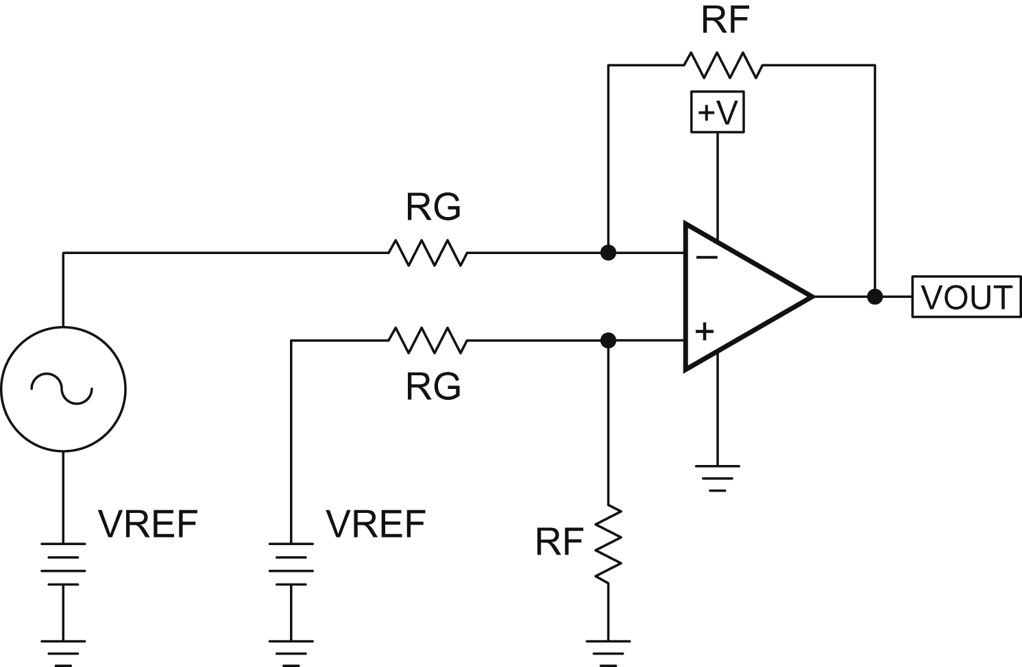
The inverting circuit shown in Fig. 4.3 is analyzed first.
Before delving directly into the math, I will take a step back and do thought experiments so the equations below make a bit more sense. The reference input above is a voltage divider to ground, therefore the DC operating point is set by that voltage divider. The DC gain on VREF is determined by that voltage divider, and by RF and RG on the inverting side (remembering that you can short the independent voltage source for the analysis). The inverting AC gain, meanwhile, is set by RF and RG in the bottom leg of the circuit. Putting these thoughts down algebraically:

Eq. (4.1) is written with the aid of superposition, and simplified algebraically, to acquire Eq. (4.2).
For VREF = VIN, one obtains Eq. (4.3), and there is no output voltage from the circuit regardless of the input voltage.
When VREF = 0, VOUT = −VIN(RF/RG), there are two possible solutions to Eq. (4.2). First, when VIN is any positive voltage, VOUT should be negative voltage. The circuit cannot achieve a negative voltage with a positive supply, so the output saturates at the lower power supply rail. Second, when VIN is any negative voltage, the output spans the normal range according to Eq. (4.5).
When VREF equals the supply voltage, VCC, we obtain Eq. (4.6). In Eq. (4.6), when VIN is negative, VOUT should exceed VCC; that is impossible, so the output saturates. When VIN is positive, the circuit acts as an inverting amplifier.
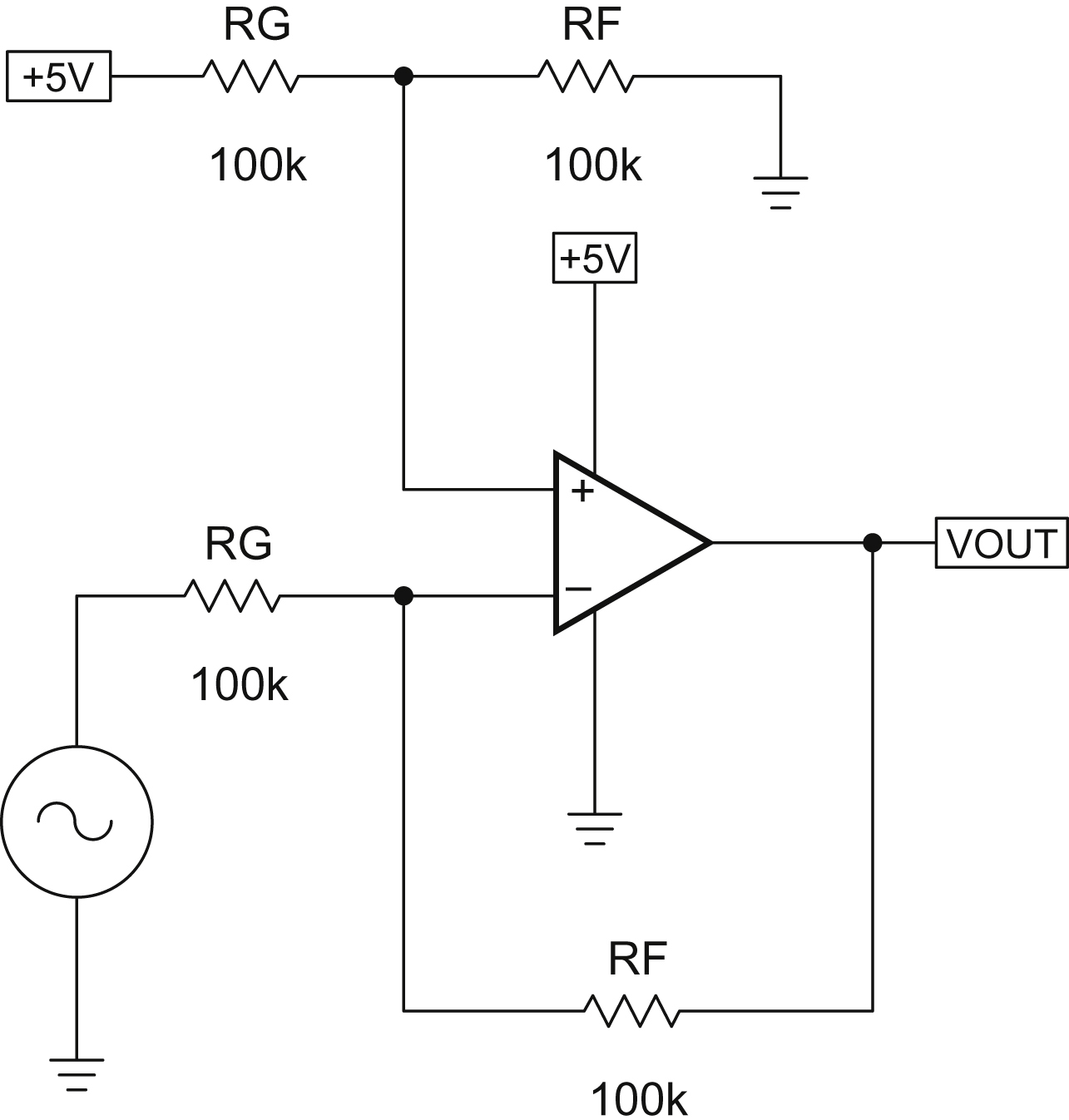
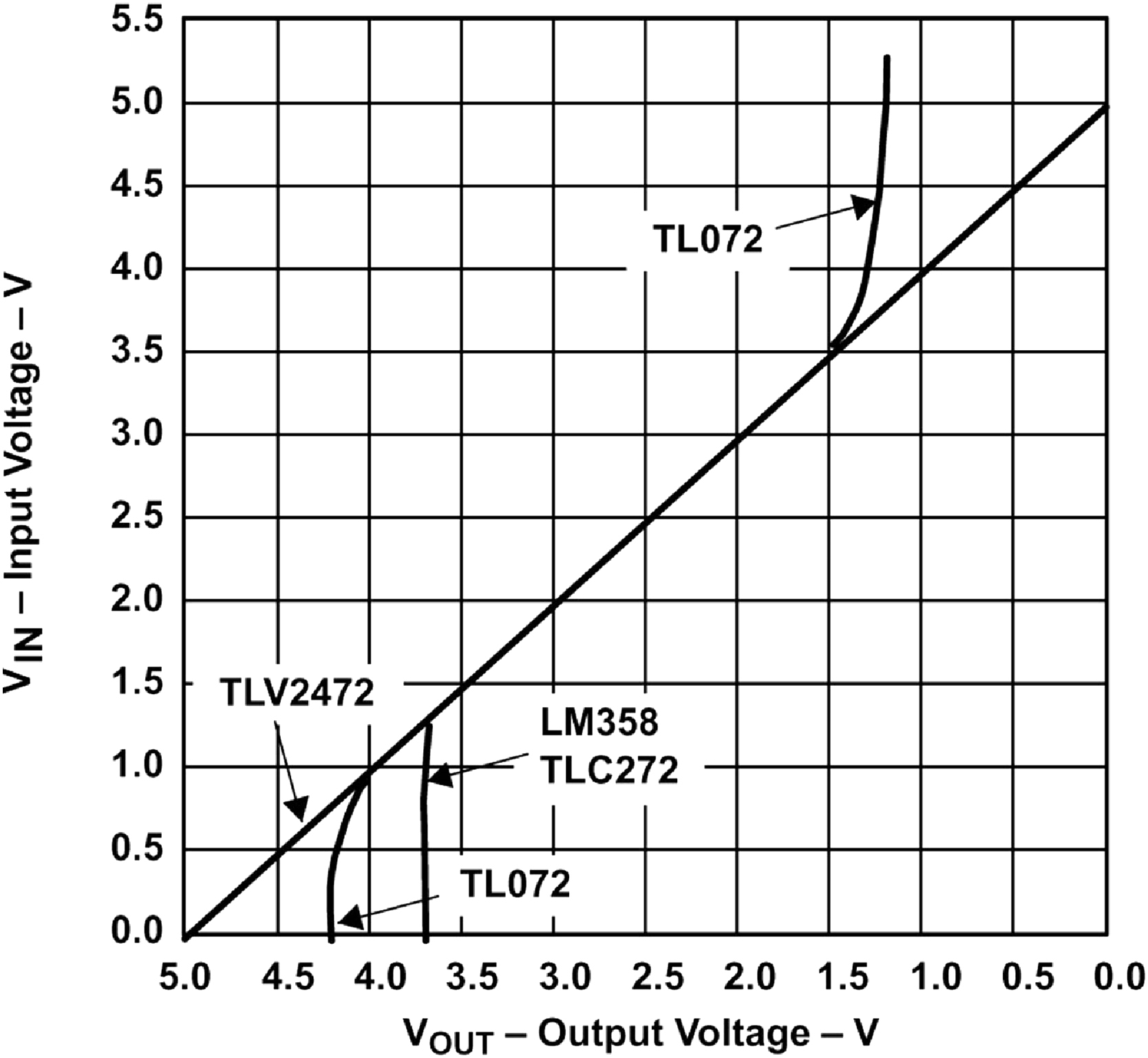
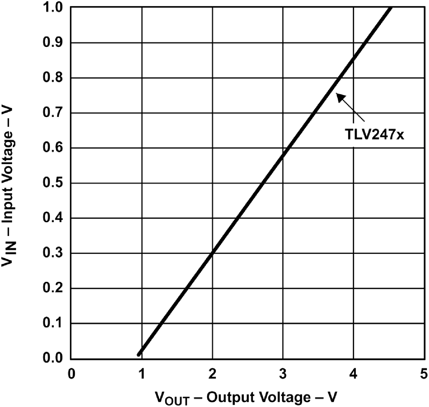
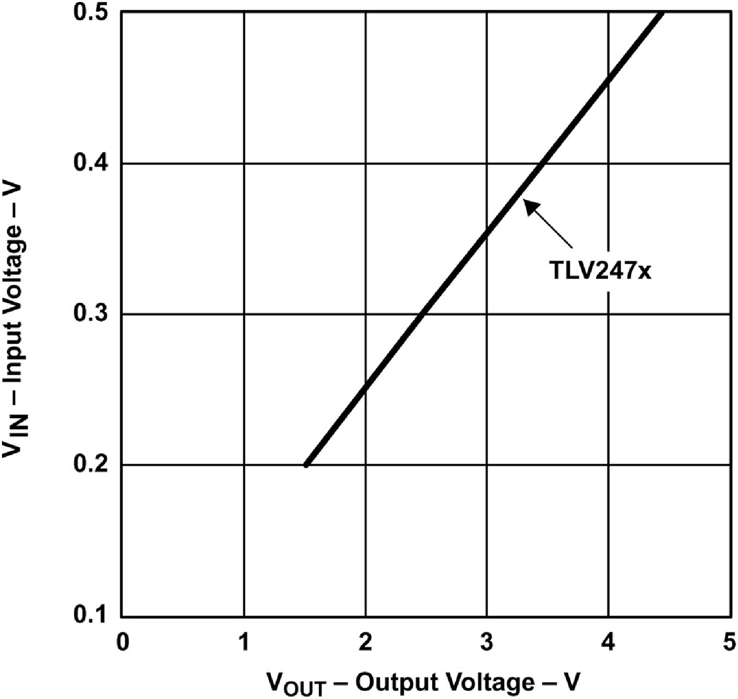
Four op amps were tested in the circuit configuration shown in Fig. 4.4. Three op amps, LM358, TL07X, and TLC272, had output voltage spans of 2.3–3.75 V. This performance does not justify the ideal op amp assumption that was made in the previous chapter unless the output voltage swing is severely limited. Limited output or input voltage swing is one of the worst deficiencies a single-supply op amp can have because the limited voltage swing limits the circuit's dynamic range. Also, limited voltage swing frequently results in distortion of large signals. The fourth op amp tested was the TLV247X, which was designed for rail-to-rail operation in single-supply circuits. The TLV247X plotted a perfect curve (results limited by the instrumentation) and performance that justifies the use of ideal assumptions. Some of the older op amps must limit their transfer equation as shown in Eq. (4.7).
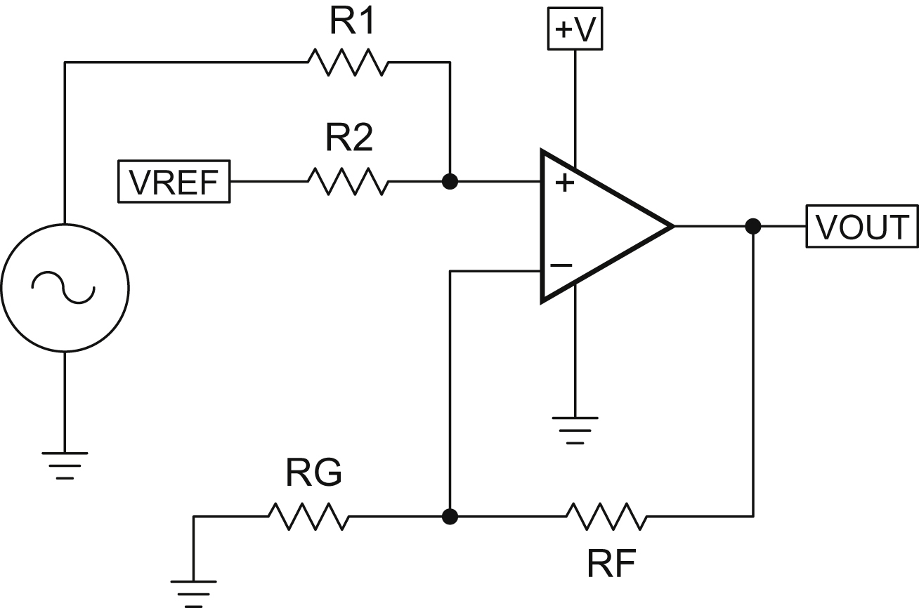
The noninverting op amp circuit is shown in Fig. 4.6.
The only difference between Figs. 4.6 and 4.3 is that the relative positions of the input signal and VREF have been swapped. Therefore, the gain on VREF is determined by RF and RG in the bottom leg of the circuit, and the signal gain is determined by voltage divider composed of RF and RG in the top leg of the circuit, times gain provided by RF and RG in the bottom leg.

Eq. (4.8) is written with the aid of superposition, and simplified algebraically, to acquire Eq. (4.9).
When  there are two possible circuit solutions. First, when VIN is a negative voltage, VOUT must be a negative voltage. The circuit cannot achieve a negative output voltage with a positive supply, so the output saturates at the lower power supply rail. Second, when VIN is a positive voltage, the output spans the normal range as shown by Eq. (4.11).
The noninverting op amp circuit shown in Fig. 4.6 is constructed with VCC = 5 V, RG = RF = 100 kΩ. The transfer curve for this circuit is shown in Fig. 4.7; a TLV247X serves as the op amp.
There are many possible variations of inverting and noninverting circuits. At this point many designers analyze these variations hoping to stumble upon the one that solves the circuit problem. A design methodology is needed, one that is guaranteed to provide the correct circuit configuration each and every time. Fortunately, there is such a methodology, and it comes from the realm of the Cartesian coordinate system. This uniform design methodology starts by employing simultaneous equations to render specified data into equation form. When the form of the desired equation is known, a circuit that fits the equation can be chosen to solve the problem. The resulting equation must be a straight line, thus there are only four possible solutions.

4.4. Simultaneous Equations
Taking an orderly path to developing a circuit that works the first time starts here; follow these steps until the equation of the op amp is determined. Use the specifications given for the circuit coupled with simultaneous equations to determine what form the op amp equation must have. Go to the section that illustrates that equation form (called a case), solve the equation to determine the resistor values, and you have a working solution.
A linear op amp transfer function is limited to the equation of a straight line (Eq. 4.12).
The equation of a straight line has four possible solutions depending upon the sign of the slope “m,” and the intercept “b”; thus simultaneous equations yield solutions in four forms. Four circuits must be developed; one for each form of the equation of a straight line. The four equations, cases, or forms of a straight line are given in Eqs. (4.13) through (4.16), where electronic terminology has been substituted for math terminology.
Only two points are required to determine a line, so given two data points for VOUT and VIN, simultaneous equations are solved to determine m and b for the equation that satisfies the given data. The sign of m and b determines the type of circuit required to implement the solution.
An example:
Circuit requirement: “A sensor output signal ranging from 0.1 V to 0.2 V must be interfaced into an analog-to-digital converter that has an input voltage range of 1 V to 4 V.”
This requirement generates the two required data points to determine a straight line:
1. VOUT = 1 V at VIN = 0.1 V
2. VOUT = 4 V at VIN = 0.2 V
This is all we need to generate the simultaneous equations and solve for the straight line, circuit topology, and component values!
The data points are inserted into Eq. (4.13), as shown in Eqs. (4.17) and (4.18), to obtain m and b for the specifications.
Multiply Eq. (4.17) by 2 and subtract it from Eq. (4.18).
After algebraic manipulation of Eq. (4.17), substitute Eq. (4.20) into Eq. (4.17) to obtain Eq. (4.21).
Now m and b are substituted back into Eq. (4.13) yielding Eq. (4.22).
Notice, although Eq. (4.13) was the starting point, the form of Eq. (4.22) is identical to the format of Eq. (4.14). The specifications or given data determine the sign of m and b, and starting with Eq. (4.13), the final equation form is discovered after m and b are calculated. The next step required to complete the problem solution is to develop a circuit that has an m = 30 and b = −2. If we so desired, we could now go to Section 4.4.2—the Case 2 section, to complete the design. But this example was only meant to illustrate how to determine the case, Section 4.4.2 describes a solution for a very similar case.
Circuits were developed for Eqs. (4.13) through (4.16), and they are given under the headings Case 1 through Case 4 respectively. There are different circuits that will yield the same equations, but these circuits were selected because they do not require negative references.
4.4.1. Case 1: VOUT = +mVIN + b
The circuit configuration that yields a solution for Case 1 is shown in Fig. 4.8. If you look carefully at the circuit, hopefully something stands out! Both the input signal and the voltage reference are connected (through resistors) to the noninverting “+” input. Both “m” and “b” in the Case 1 equation are positive. This should be an “aha” moment, because this will hold true for the other cases. However, there is much analysis to be done before you can determine the exact circuit schematic and the exact component values. But your understanding should be enhanced at this point.
Another thing that should stand out to you is that the noninverting input configuration is nothing more than a summer circuit, with a noninverting gain determined by RF and RG. But be careful, it would be easy to underestimate the task at this point! R1 and R2 are also voltage dividers on the input signal and VREF, respectively!
The circuit equation is written using the voltage divider rule and superposition.
The equation of a straight line (case 1) is repeated in Eq. (4.24) below so comparisons can be made between it and Eq. (4.23).
A Case 1 Example:
The circuit specifications are as follows:
1. VOUT = 1 V at VIN = 0.01 V
2. VOUT = 4.5 V at VIN = 1 V
As before, this is all we need to complete the design. Except for two details—the supply and reference voltage. Sometimes, no reference voltage is available, and it is necessary to use the supply voltage. A reference voltage source is left out of the design as a space and cost savings measure, and it sacrifices noise performance, accuracy, and stability performance. Cost is an important specification, but the VCC supply must be specified well enough to do the job. Assume for this example that +5 V is used for both supply and reference.
Each step in the subsequent design procedure is included in this analysis to ease. Many steps will be skipped when subsequent cases are analyzed.
The data are substituted into simultaneous equations.
Eq. (4.27) is multiplied by 100 (Eq. 4.29) and Eq. (4.28) is subtracted from Eq. (4.29) to obtain Eq. (4.30).
The slope of the transfer function, m, is obtained by substituting b into Eq. (4.27).
Now that b and m are calculated, the resistor values can be calculated. Eqs. (4.25) and (4.26) are solved for the quantity (RF + RG)/RG, and then they are set equal in Eq. (4.32) thus yielding Eq. (4.33).
 (4.33)
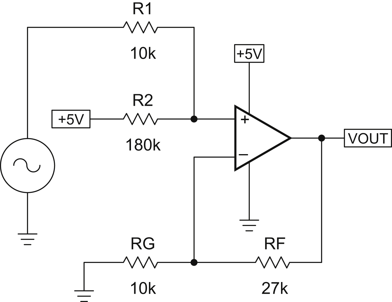
Choose R1 = 10 kΩ, and that sets the value of R2 = 183.16 kΩ. The closest 5% resistor value to 183.16 kΩ is 180 kΩ; therefore, select R1 = 10 kΩ and R2 = 180 kΩ. Being forced to yield to reality by choosing standard resistor values means that there is an error in the circuit transfer function, because m and b are not exactly the same as calculated. The real world constantly forces compromises into circuit design, but the good circuit designer accepts the challenge and throws money or brains at the challenge. Using 10 cent resistors with a 10 cent op amp is hard to justify except in precision circuits; however, the price of 1% resistors has plummeted in recent years, and there is seldom a need to make such a compromise today.
The left half of Eq. (4.32) is used to calculate RF and RG.
The resulting circuit equation is given below.
The gain setting resistor, RG, is selected as 10 kΩ, and 27 kΩ, the closest 5% standard value is selected for the feedback resistor, RF. Again, there is a slight error involved with standard resistor values. This circuit must have an output voltage swing from 1 to 4.5 V. The circuit with the selected component values is shown in Fig. 4.9 and the transfer curve is shown in Fig. 4.10.
The transfer curve shown is a straight line, and that means that the circuit is linear. The VOUT intercept is about 0.98 V rather than 1 V as specified, and this is excellent performance considering that the components were selected from 5% resistor values. The output voltage measured 4.53 V when the input voltage was 1 V. Considering the low and high input voltage errors, it is safe to conclude that the resistor tolerances have skewed the gain slightly, but this is still excellent performance for 5% components. Often lab data similar to that shown here are more accurate than the 5% resistor tolerance, but do not fall into the trap of expecting this performance, because you will be disappointed if you do.
The resistors were selected in the kΩ range arbitrarily. The gain and offset specifications determine the resistor ratios, but supply current, frequency response, and op amp drive capability determine their absolute values. The resistor value selection in this design is high because modern op amps do not have input current offset problems, and they yield reasonable frequency response. If higher frequency response is demanded, the resistor values must decrease, and resistor value decreases reduce input current errors, while supply current increases. When the resistor values get low enough, it becomes hard for another circuit, or possibly the op amp, to drive the resistors.
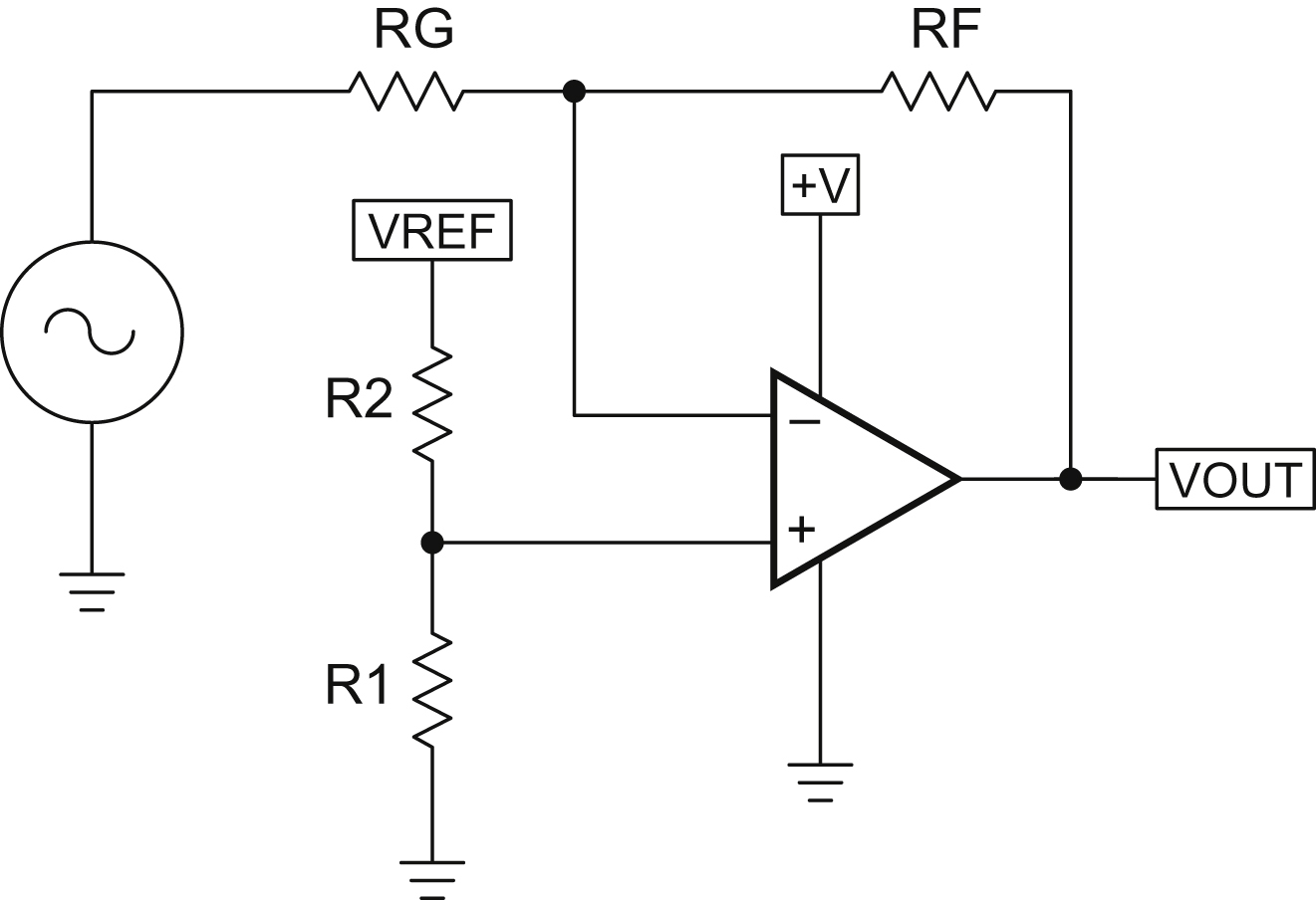
4.4.2. Case 2: VOUT = +mVIN − b
The circuit shown in Fig. 4.11 yields a solution for Case 2. Before delving into the math, let us take a broad view of what is going on. The slope m is positive, so the input signal is applied to the noninverting input. The intercept b is negative, so it is applied to the inverting input. Noninverting gain for the signal input is provided by RF and RG, and inverting gain for the reference is also provided by RF and RG. At this point, though, you should be noticing a fundamental limitation of this circuit. There will be some error introduced by the resistors R1 and R2, which form a voltage divider off of +VREF. This error can be mitigated somewhat by making the scale of the resistors RG and RF large in comparison with R1 and R2—say 100 times the value. This is the most problematic solution for the four cases presented in this chapter. If you were concerned only with AC response on the input signal, you could bypass R2 with a capacitor, but we are assuming in this chapter that you are concerned with DC response—so that will not work. The best solution would be to use a separate op amp to buffer R1 and R2, thus presenting a low impedance to RG. Indeed, the price of dual op amps, and the packages they are offered in, may make this a viable solution. But for the sake of this analysis, we will proceed with the assumption that only a single op amp is available. The solution it yields is surprisingly satisfactory!

The circuit equation is obtained by taking the Thevenin equivalent circuit looking into the junction of R1 and R2. After the R1, R2 circuit is replaced with the Thevenin equivalent circuit, the gain is calculated with the ideal gain equation (Eq. 4.37).
The specifications for an example design are VOUT = 1.5 V at VIN = 0.2 V, VOUT = 4.5 V at VIN = 0.5 V, and VREF = VCC = 5 V. The simultaneous equations, Eqs. 4.40 and 4.41, are written below.
From these equations we find that b = −0.5 and m = 10. Making the assumption that R1‖R2 << RG simplifies the calculations of the resistor values.
Let RG = 20 kΩ, and then RF = 180 kΩ.
Select R2 = 820 Ω, and R1 equals 72.98 kΩ. Since 72.98 kΩ is not a standard 5% resistor value, R1 is selected as 75 kΩ. The difference between the selected and calculated value of R1 has about a 3% effect on b, and this error shows up in the transfer function as an intercept rather than a slope error. The parallel resistance of R1 and R2 is approximately 820 Ω and this is much less than RG, which is 20 kΩ, thus the earlier assumption that RG >> R1‖R2 is justified. The final circuit is shown in Fig. 4.12 and the measured transfer curve for this circuit is shown in Fig. 4.13. Notice that I went ahead and added the capacitor across R2. This is not for AC gain, although it would certainly have that effect. It is merely there for bypassing on the DC potential that generates the intercept b, to reduce noise (since we are using the power supply as +VREF).

The TLV247X was used to build the test circuit because of its wide dynamic range. The transfer curve plots are very close to the theoretical curve; the direct result of using a high performance op amp.
4.4.3. Case 3: VOUT = −mVIN + b
The circuit shown in Fig. 4.14 yields the transfer function desired for Case 3. This is really straightforward. The intercept is positive; it is applied to the noninverting input. The slope is negative; it is applied to the inverting input. The inverting gain on the signal is simple, being determined by RF and RG. The reference voltage goes through a voltage divider and then has noninverting gain determined by RF and RG.
The circuit equation is obtained with superposition.
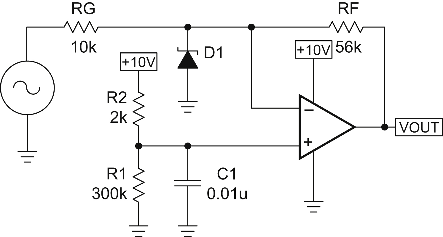
The design specifications for an example circuit are VOUT = 1 V at VIN = −0.1 V, VOUT = 6 V at VIN = −1 V, and VREF = VCC = 10 V.
Up until now, we have been using a TLV247 family op amp for our real world circuits. Let us complicate things a bit! The supply voltage available for this circuit is 10 V, and this exceeds the maximum allowable supply voltage for the TLV247X. Also, assume this circuit must drive a back-terminated cable that looks like two 50 Ω resistors connected in series, thus the op amp must be able to drive 6/100 = 60 mA. The stringent op amp selection criteria limits the of op amps if ideal op amp equations are going to be used. The TLC07X has excellent single-supply input performance coupled with high output current drive capability, so it is selected for this circuit.
From these equations we find that b = 0.444 and m = −5.6.
Let RG = 10 kΩ, and then RF = 56.6 kΩ, which is not a standard 5% value, hence RF is selected as 56 kΩ.
The final equation for the example is given below.
Select R1 = 2 kΩ and R2 = 295.28 kΩ. Since 295.28 kΩ is not a standard 5% resistor value, R1 is selected as 300 kΩ. The difference between the selected and calculated value of R1 has a nearly insignificant effect on b. The final circuit is shown in Fig. 4.15, and the measured transfer curve for this circuit is shown in Fig. 4.16.
There could be an issue that would destroy the op amp. As long as the circuit works normally, there are no problems handling the negative voltage input to the circuit, because the inverting lead of the TLC07X is at a positive voltage. The positive op amp input lead is at a voltage of approximately 65 mV, and normal op amp operation keeps the inverting op amp input lead at the same voltage because of the assumption that the error voltage is zero. However, when VCC is powered down while there is a negative voltage on the input circuit, most of the negative voltage appears on the inverting op amp input lead.

The most prudent solution is to connect the diode, D1, with its cathode on the inverting op amp input lead and its anode at ground. If a negative voltage gets on the inverting op amp input lead, it is clamped to ground by the diode. Select the diode type as Schottky, so the voltage drop across the diode is about 200 mV; this small voltage does not harm most op amp inputs. As a further precaution, RG can be split into two resistors with the diode inserted at the junction of the two resistors. This places a current limiting resistor between the diode and the inverting op amp input lead.
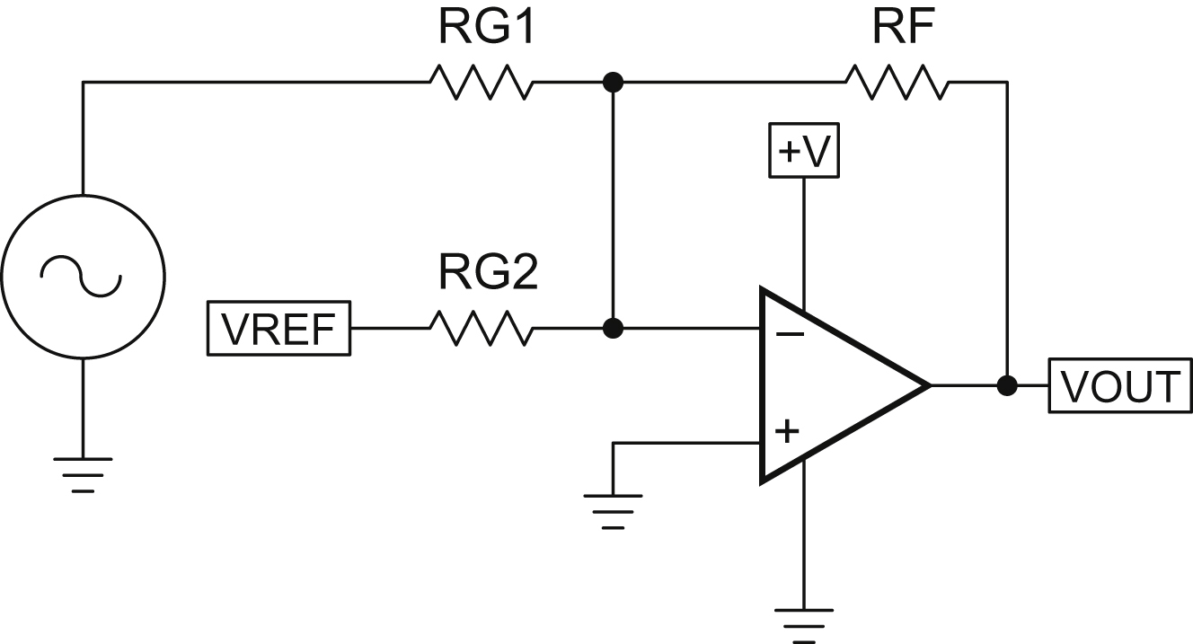
4.4.4. Case 4: VOUT = −mVIN − b
The circuit shown in Fig. 4.17 yields a solution for Case 4. As you can see, because both the slope m and intercept b are negative, both are applied to the inverting input. Furthermore, Case 4 reduces to that of the simple summation circuit described in an earlier chapter. The final solution, however, must take some other things into account to avoid turnoff problems like those described in Case 3.
The circuit equation is obtained by using superposition to calculate the response to each input. The individual responses to VIN and VREF are added to obtain Eq. (4.56).
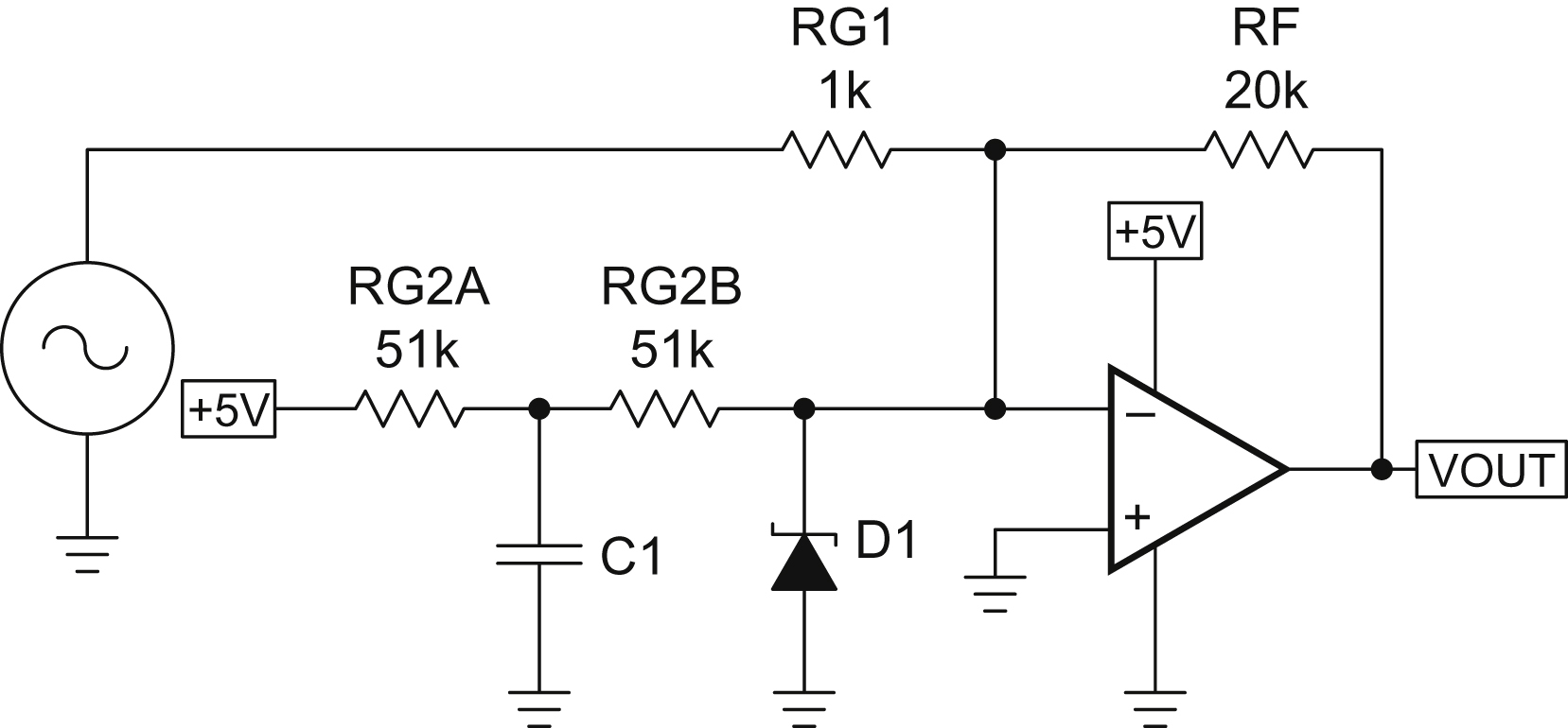
The design specifications for an example circuit are: VOUT = 1 V at VIN = −0.1 V, VOUT = 5 V at VIN = −0.3 V, VREF = VCC = 5 V, RL = 10 kΩ, and 5% resistor tolerances. The simultaneous equations, Eqs. (4.59) and (4.60), are written below.
From these equations we find that b = −1 and m = −20. Setting the magnitude of m equal to Eq. (4.57) yields Eq. (4.61).
Let RG1 = 1 kΩ, and then RF = 20 kΩ.
The final equation for this example is given in Eq. (4.63).
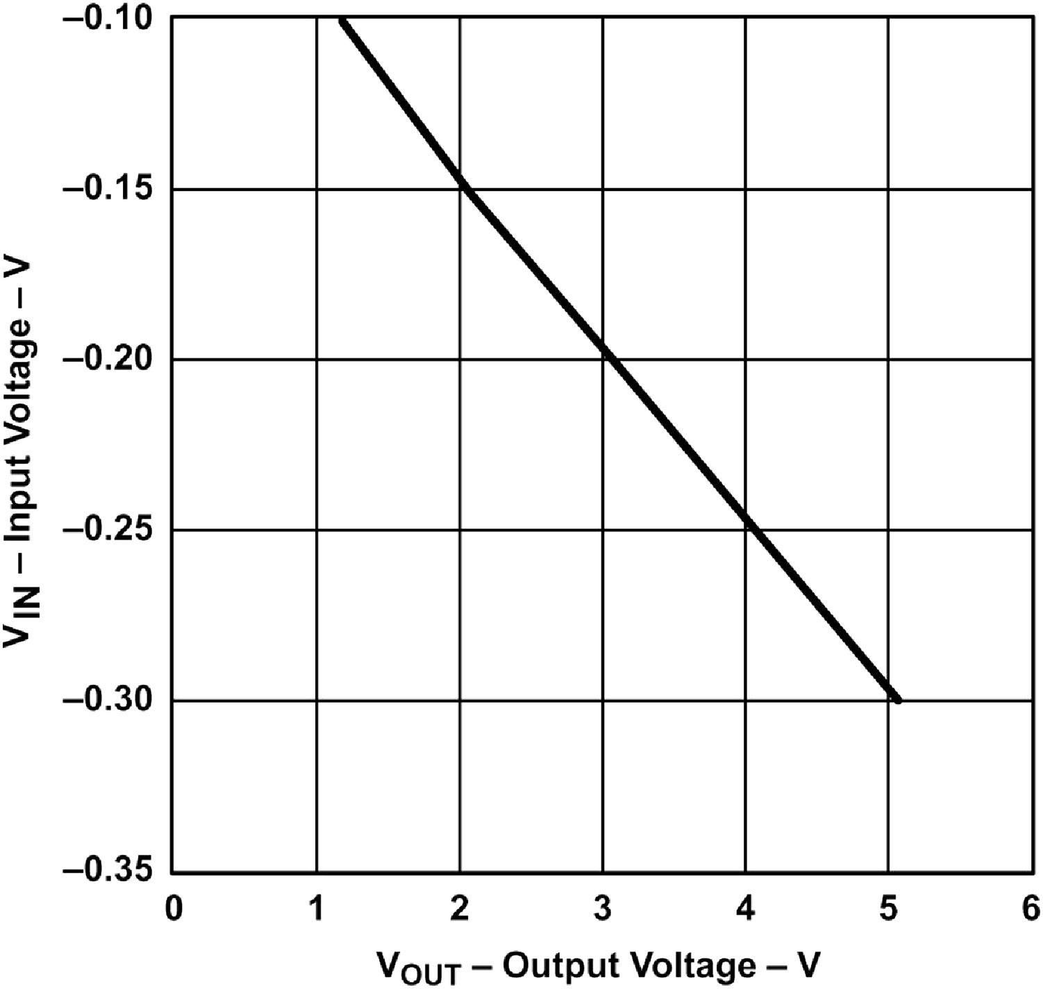
The final circuit is shown in Fig. 4.18 and the measured transfer curve for this circuit is shown in Fig. 4.19.
The TLV247X was used to build the test circuit because of its wide dynamic range. The transfer curve plots very close to the theoretical curve.
As in Case 3, as long as the circuit works normally there are no problems handling the negative voltage input to the circuit because the inverting lead of the TLV247X is at a positive voltage. The positive op amp input lead is grounded, and normal op amp operation keeps the inverting op amp input lead at ground because of the assumption that the error voltage is zero. When VCC is powered down while there is a negative voltage on the inverting op amp input lead there is a possibility of circuit damage.
The most prudent solution is to connect the diode, D1, with its cathode on the inverting op amp input lead and its anode at ground. If a negative voltage gets on the inverting op amp input lead it is clamped to ground by the diode. Select the diode type as germanium or Schottky, so the voltage drop across the diode is about 200 mV; this small voltage does not harm most op amp inputs. RG2 is split into two resistors (RG2A = RG2B = 51 kΩ) with a capacitor inserted at the junction of the two resistors. This decouples VCC.
4.5. Summary
Single-supply op amp design is more complicated than split-supply op amp design, but with a logical design approach excellent results are achieved. Single-supply design used to be considered technically limiting because older op amps had limited capability. Op amps such as the TLC247X, TLC07X, and TLC08X have excellent single-supply parameters; thus when used in the correct applications these op amps yield rail-to-rail performance equal to their split-supply counterparts.
Single-supply op amp design usually involves some form of biasing, and this requires more thought, so single-supply op amp design needs discipline and a procedure. The recommended design procedure for single-supply op amp design is as follows:
• Substitute the specification data into simultaneous equations to obtain m and b (the slope and intercept of a straight line).
• Let m and b determine the form of the circuit.
• Choose the circuit configuration that fits the form.
• Using the circuit equations for the circuit configuration selected, calculate the resistor values.
• Build the circuit, take data, and verify performance.
• Test the circuit for nonstandard operating conditions (circuit power off while interface power is on, over/under range inputs, etc.).
• Add protection components as required.
• Retest.
When this procedure is followed, good results follow. As single-supply circuit designers expand their horizon, new challenges require new solutions. Remember, the only equation a linear op amp can produce is the equation of a straight line. That equation only has four forms. The new challenges may consist of multiple inputs, common-mode voltage rejection, or something different, but this method can be expanded to meet these challenges.
..................Content has been hidden....................
You can't read the all page of ebook, please click here login for view all page.