
16.7. All-Pass Filter Design
In comparison to the previously discussed filters, an all-pass filter has a constant gain across the entire frequency range, and a phase response that changes linearly with frequency.
Because of these properties, all-pass filters are used in phase compensation and signal delay circuits.
Similar to the low-pass filters, all-pass circuits of higher order consist of cascaded first-order and second-order all-pass stages. To develop the all-pass transfer function from a low-pass response, replace A0 with the conjugate complex denominator.
The general transfer function of an all-pass is
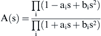 (16.23)
with ai and bi being the coefficients of a partial filter. The all-pass coefficients are listed in Table 16.12 of Section 16.9.
Expressing Eq. (16.23) in magnitude and phase yields
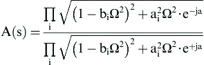 (16.24)
This gives a constant gain of 1, and a phase shift,φ, of:
To transmit a signal with minimum phase distortion, the all-pass filter must have a constant group delay across the specified frequency band. The group delay is the time by which the all-pass filter delays each frequency within that band.
The frequency at which the group delay drops to  times its initial value is the corner frequency, fC.
The group delay is defined through:
To present the group delay in normalized form, refer tgr to the period of the corner frequency, TC, of the all-pass circuit:
Substituting tgr through Eq. (16.26) gives
Inserting the φ term in Eq. (16.25) into Eq. (16.28) and completing the derivation, results in:
 (16.29)
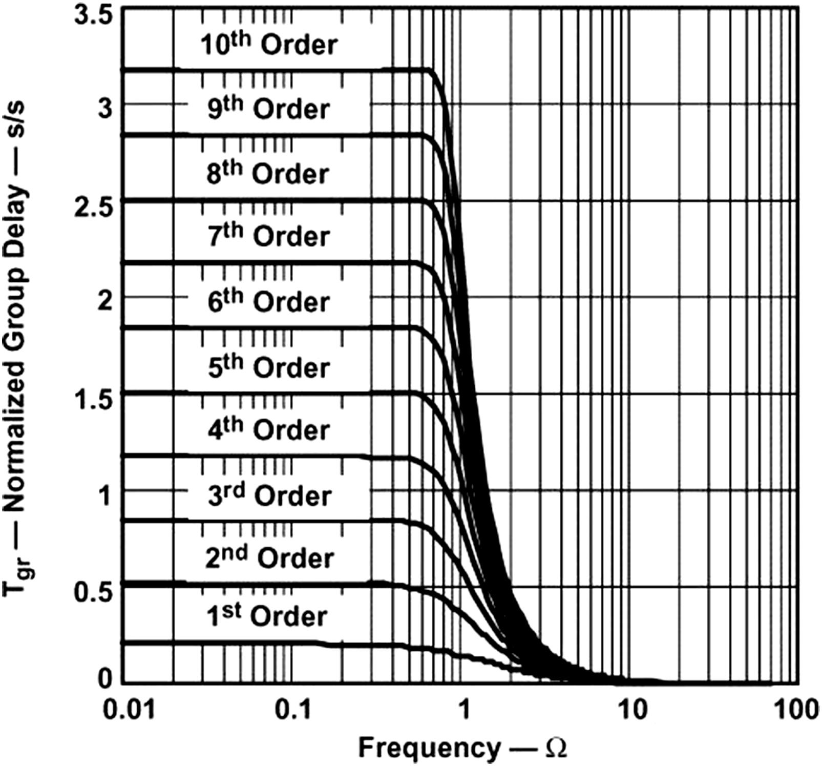
The values for Tgr0 are listed in Table 16.12, Section 16.9, from the first to the tenth order.
In addition, Fig. 16.42 shows the group delay response versus the frequency for the first ten orders of all-pass filters.
16.7.1. First-Order All-Pass Filter
Fig. 16.43 shows a first-order all-pass filter with a gain of +1 at low frequencies and a gain of −1 at high frequencies. Therefore, the magnitude of the gain is 1, while the phase changes from 0 degrees to −180 degrees.
The transfer function of the circuit above is
To design a first-order all-pass, specify fC and C and then solve for R:
Inserting Eq. (16.31) into Eq. (16.30) and substituting ωC with Eq. (16.27) provides the maximum group delay of a first-order all-pass filter:
16.7.2. Second-Order All-Pass Filter
Fig. 16.44 shows that one possible design for a second-order all-pass filter is to subtract the output voltage of a second-order band-pass filter from its input voltage.
The transfer function of the circuit in Fig. 16.44 is
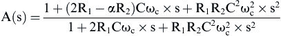


The coefficient comparison with Eq. (16.23) yields
To design the circuit, specify fC, C, and R, and then solve for the resistor values:
Inserting Eq. (16.34) into Eq. (16.30) and substituting ωC with Eq. (16.27) gives the maximum group delay of a second-order all-pass filter:
16.7.3. Higher-Order All-Pass Filter
Higher-order all-pass filters consist of cascaded first-order and second-order filter stages.
Example 16.7. 2-ms Delay All-Pass Filter.
A signal with the frequency spectrum, 0 < f < 1 kHz, needs to be delayed by 2 ms. To keep the phase distortions at a minimum, the corner frequency of the all-pass filter must be fC ≥ 1 kHz.
Eq. (16.27) determines the normalized group delay for frequencies below 1 kHz:
Fig. 16.42 confirms that a seventh-order all-pass is needed to accomplish the desired delay. The exact value, however, is Tgr0 = 2.1737. To set the group delay to precisely 2 ms, solve Eq. (16.27) for fC and obtain the corner frequency:
To complete the design, look up the filter coefficients for a seventh-order all-pass filter, specify C, and calculate the resistor values for each partial filter.
Cascading the first-order all-pass with the three second-order stages results in the desired seventh-order all-pass filter (See Fig. 16.45).
..................Content has been hidden....................
You can't read the all page of ebook, please click here login for view all page.