
Chapter 13
Troubleshooting—What to Do When Things Go Wrong
Abstract
Troubleshooting op amp circuits sometimes involves correcting commonly made, simple mistakes. Checking power connections, enabling pin requirements, checking the DC operating point are the simplest. A designer oftentimes tries to get too much gain out of a single amplifier. Fixing noisy circuits is more involved. Noise conducted and radiated into and out of the circuit need to be checked. DC offset is also addressed.
Keywords
Conducted emissions; Conducted susceptibility; DC offset; Enable requirements; Power requirements; Radiated emissions; Radiated susceptibility
13.1. Introduction
You now have a good understanding of the basics of op amp design. Before wandering off into op amp applications, I thought I would take time to offer some guidance to those of you who have a circuit and it does not work or does not work properly. This has been the number one most requested topic for the fifth edition of Op Amps for Everyone, and I will strive not to disappoint. I should tell you right up front, there is no such thing as an exhaustive list of fixes. As soon as I come up with a fix for one application, another, different problem will arise, sometimes in the same circuit! After handling hundreds of applications inquiries, and being a designer myself on dozens if not hundreds of circuits, I believe that I have invented quite a few ways of messing things up. We all learn as much from our failures as by our successes (at least those of us who are wise enough to do so). A design failure should be looked at as an opportunity to learn something new—you have learned one more thing that does not work—not as a personal failure or proof of your incompetence. If only management and other team members could always be so enlightened!
13.2. Simple Things First—Check the Power!
Even with close to 40 years of experience, you would be surprised at the number of times I have simply forgotten to hook up the power! Or I have done something that mangles the power. This is easy to do if a CAD program is incorrectly applied. If the power pins are not shown on the op amp, and have to be separately placed—it is easy to forget them! The very first step when the circuit is not operating—or not doing what you expect—is to check the power pins of the op amp. If you are operating split supply, the positive power input should be the positive analog voltage you are supplying to the op amp. And the negative power input should be the negative analog voltage you are supplying to the op amp. If you are operating single supply, the negative voltage terminal of the op amp should be at ground. Verifying this should be the first thing you do because nothing is going to be right without power. There are sneak paths and leakage paths that can allow a circuit to have an output, just not the right one, or not a good one with no power applied. It is easy to mistake this for a bad circuit—or failed op amp—when all that is wrong is that power is not properly applied.
13.3. Do Not Forget That Enable Pin
This can be a sneaky one, because not all enables are created equal. In a split supply system, it may be referenced to the negative supply voltage, not to ground. This makes it difficult to interface to microcontrollers or other logic sources. Some enable pins can be left open if not used, others must be tied to a potential. Suffice it to say, if you are using an op amp with an enable pin, read the data sheet carefully to make sure you have utilized it correctly.
13.4. Check the DC Operating Point
Remember in our discussion of the ideal op amp, I gave you all op amp theory in one sentence: “The output will do whatever it has to do to make the two input voltages equal.” This is also an excellent troubleshooting technique. With no signal input, apply power and check the output, the inverting input, and the noninverting input. If they are not all at the same level, or very close to the same level, something is wrong. This holds true for split supply circuits or single supply circuits.
• If the output is near the positive supply voltage, the noninverting input is probably higher than the inverting input, and for some reason the op amp cannot equalize the two inputs.
• If the output is near the negative supply voltage, the inverting input is probably higher than the noninverting input, and again for some reason the op amp cannot equalize the two inputs.
This is called “hitting the rail,” and obviously the circuit will not operate in this configuration. If it responds to an AC signal at all, part of the output waveform will be clamped to a DC potential, while the other excursion may be present in part. This is oftentimes caused by too much gain amplifying the input offset voltage. Or perhaps, if this is an AC application, one of the DC blocking capacitors has been forgotten. Even in a split supply circuit, it is oftentimes easy to eliminate the DC offset by proper application of DC blocking capacitors.
13.5. The Gain Is Wrong
You should not have this problem, if you have been reading this book, especially Section 7.6. Assuming that you do not have a broken resistor somewhere, you should double check the open loop gain of your op amp. You may have run out of operating room, and need to select another. With hundreds of op amps on the market, chances are good you can find one with more open loop bandwidth and therefore more operating room where you need it. If not, you are going to consider two op amp stages, and divide up your gain between them. This is probably not a disaster, because many op amps come in dual versions, which would be more passive components but still only one IC.
13.6. The Output Is Noisy
All semiconductors generate noise, this is just the nature of the semiconductor physics involved. With that said, there can be a number of reasons why your circuit generates excessive noise. I cover the subject of op amp noise in Appendix C if you want more information. Op amp noise is dependent on frequency, you can always look at a different op amp with different noise specifications. Before spending money on an expensive low noise op amp, you should rule out external noise sources.
For now, I will cover the topic of noise from the standpoint of military specifications—at least in broad, general terms. There are four categories of noise:
• Conducted emissions—noise produced by the circuit conducted to other places over power or signal connections.
• Conducted susceptibility—noise produced elsewhere in the circuit that gets conducted into the op amp stage over power or signal connections.
• Radiated emissions—noise produced by the circuit that radiates wirelessly to other parts of the system.
• Radiated susceptibility—external RF noise that affects the circuit.
Let us look at these separately, and establish protocols to deal with them.
First and foremost, make sure your power pins—including the reference if used—are bypassed. This is your first line of defense. Proper bypassing does not mean slapping a 0.1 μF capacitor on the power pin. I will have a lot more to say about this later, but at least read the data sheet and follow any specific recommendations. That is a starting point, not the finishing point of bypassing.
13.6.1. Conducted Emissions and Radiated Emissions
If you have either of these conditions, you have my sympathy, because you probably have a completely unfunctional circuit. You have probably loaded down the output with capacitance, making the stage unstable, or you have completely ignored and violated stability criteria. A thorough reevaluation of your circuit is the only cure, with special emphasis on stability. Even I occasionally hang too much capacitance on an op amp output and it oscillates. Or I forget that I have selected a gain of 10 stable op amps, and am using it at a gain of one. An oscillating circuit will put noise on the power lines, conducting to other stages, or it will actually broadcast, and you better fix that before encountering the Federal Communications Commission (FCC)!
The most common reason for too much capacitance on an output is the presence of a coax cable. Think of a coaxial cable as long, skinny capacitor. Loading an op amp that is not designed to drive capacitive loads with a capacitor will never do! The simplest method of combating this is to select an op amp with the ability to drive capacitive loads. These will be advertised as such, and the capacitance they can drive will be clearly specified. However, this will severely limit the number of op amps from which you can select.
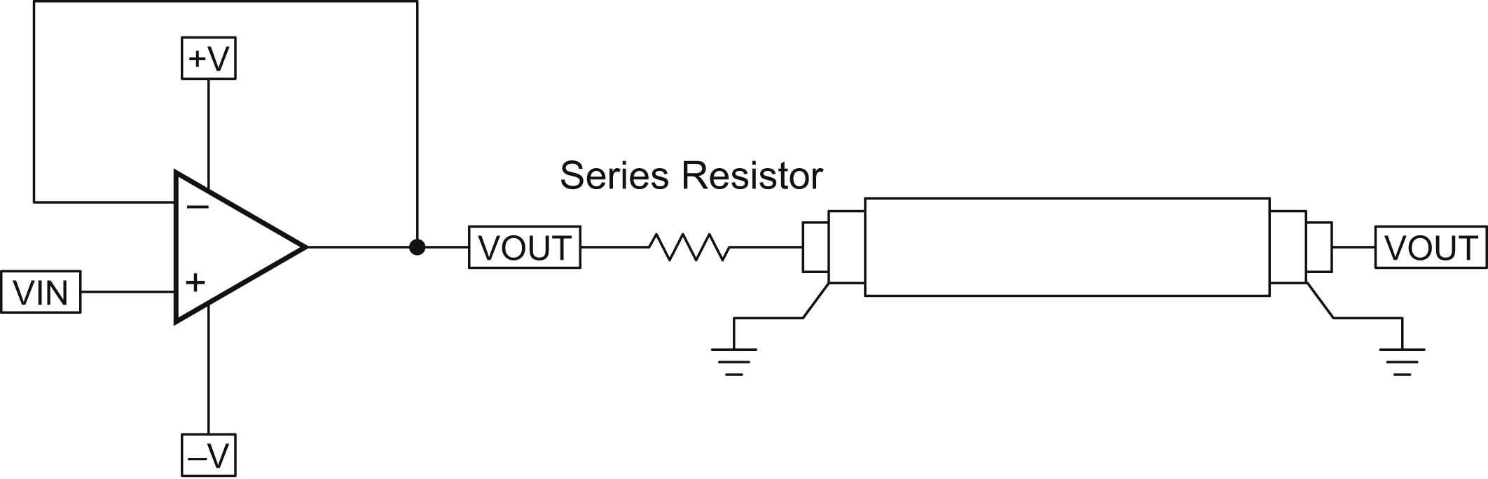
There are techniques to counter the capacitance of coaxial cable (and other capacitive loads). One of the simplest is to place a simple series resistor on the output of the op amp.
This will convert the capacitive load of the coaxial cable into the capacitor in a simple one pole low-pass filter, so you need to make sure the roll-off associated with the low-pass filter does not adversely affect the response of your system.
A lot of the coaxial cables you will encounter have a characteristic impedance of 50 Ω. For higher frequency applications, you can use this characteristic to your advantage and borrow a technique from RF design. You can create a 50 Ω balanced system. I will not go into all the particulars of such a system, which are evaluated in any number of resources on RF design but suffice it to say that it will isolate your system from many of the adverse parasitic effects of having a long cable in the system. It is much superior to the simple series resistance approach above, but comes at a cost. A 50 Ω transmission system assumes a 50 Ω series resistance at the source and depends on a 50 Ω termination resistor at the destination for impedance matching. Remembering the voltage divider rule, this means that your output voltage amplitude is divided by two. This can be countered in our simple schematic above by converting the noninverting buffer in Fig. 13.1 above to a noninverting gain of two by adding two resistors as shown in Fig. 13.2:
If RF and RG are the same value, follow the stage gain. The noninverting gain on VIN will be 2, so VOUT from the op amp stage is VIN × 2. The voltage divider consisting of the series and termination resistors form a voltage divider of ½, so VOUT ultimately equals VIN.

Fifty Ohm transmission requires an op amp that can drive a 100 Ω load, and this also limits the number of op amps that are available for use. Generally, they are going to be high-speed op amps. A number of voltage-feedback amplifiers are available with 100 Ω drive, but generally 50 Ω transmission is better done with current-feedback op amps. This is because the requirement to use a gain of two to compensate for the voltage divider effect would otherwise limit the bandwidth of a voltage-feedback op amp.
The schematic above shows a split supply, and the astute reader may already have uncovered a flaw. The op amp will have a DC offset due to its input offset voltage. This offset will hopefully be small, but if you use a current-feedback amplifier, they are not known for low offset voltage specifications. This means a DC voltage will appear at the output, and this is not a good thing because the DC voltage will also appear across the 100 Ω load. The best-case scenario is that this will waste power supply current; the worst-case scenarios include clipping on one part of the waveform or another. Be careful with the power rating of the 50 Ω matching resistors if a steady DC voltage is designed into the system!
It is far better to isolate the 50 Ω termination system with a DC blocking capacitor as shown in Fig. 13.3.
If you consult textbooks on RF design, you will probably find this DC blocking capacitor, because many of those textbooks discuss transistor stages, which have DC bias voltages on each stage that must also be blocked. The capacitor can be selected to be large enough to have minimal effect on the signal. It should be a good quality dielectric, especially if temperature of the circuit is subject to changes.

13.6.2. Radiated Susceptibility
The best piece of advice I will give you in this chapter—get that cell phone out of your shirt pocket! If you are like me, you forget this all the time while you are working in the lab. The GSM tones periodically coming out of some cell phones are powerful and can affect your circuit.
Noise, especially “oscillation,” may result from op amp instability, or from external sources being amplified by your circuit. The very first thing you should do is to terminate the input of your op amp circuit, and check the output. If the oscillation goes away, it was not oscillation at all. It was noise amplified from an external source. You may even have to put your circuit inside a Faraday cage to isolate it from external sources of noise. Before you complain about buying an expensive Faraday cage, you should know that I use a tin candy box with a ground strap soldered to the box, lid, and ground of the board. I close the lid over the power connections and scope probe lead. This makes an inexpensive and effective Faraday cage that does a good job of isolating the board inside from outside sources of radio frequency interference. If you still see sustained oscillation, your circuit is unstable and needs to be redesigned.
If your circuit must work in the lab in the presence of strong RF signals, there are some things you can do to reject RF, assuming they are much higher in frequency compared to the bandwidth you are interested in for your application.
The first simplest thing you can do is simply install a low-pass filter at the input of your circuit, designed to attenuate high frequencies while not affecting the frequencies you are interested in as shown in Fig. 13.4

I have shown the low-pass filter on a simple noninverting buffer, your application circuit can be anything you want. I have used this technique successfully to design precision transducer circuits only two miles from an antenna farm with 20 full power FM stations and a dozen full power TV stations. Without the low-pass filter, the output was completely saturated with pickup from broadcast stations, with the low-pass filter, the output was completely clean DC level. If your application frequency is closer in frequency to major broadcast facilities, this technique may not work. Also remember that cell phone. Two watts is small compared to a 5 million watt UHF TV station, but that 2 W in your pocket is also a lot closer to your application circuit!
The next thing you can do to combat RF is to slow down your op amp. Modern op amps are implemented on a single piece of silicon, and except for the very rare uncompensated amplifier and amplifiers with offset null pins, you have no access to their internal circuitry to accomplish slowing. There is a way, however, to slow down an op amp. It involves slowing down the slew rate. Fig. 13.5 shows the first stage of a voltage-feedback op amp.
VINs are the input pins of the op amp. VOUTs are connected to the next internal stage of the op amp. This is not intended to be tutorial on the exact schematic of the input stage of every op amp. It is one possible variation, there are many others. C slew rate is not a component intentionally added to the emitters of the input transistors (which have been given the name “long-tail pair” by op amp designers). C slew rate is a representation of distributed parasitic capacitance that appears in the stage, including between the bases of the transistors (or gates in the case of an FET input op amp). Power supply designers are very familiar with parasitic gate capacitance! The point here is that parasitic capacitance will happen, and it will act to limit the slew rate of the op amp, and therefore slow it down. You do not have access to the emitters of the transistors, but you do have access to the bases! They are, after all, the inputs. So if you want to intentionally slow an op amp down, all you have to do is to connect a capacitor between the two inputs as shown in Fig. 13.6.


The slew rate reduction capacitor shown above is in addition to the components of your application, of course. It is no way negates the requirement to close the loop of the op amp, I merely omitted all other components to show the addition of one part. It is also good to keep this capacitor to a few picofarads or tens of picofarads, because it can introduce noise.
13.6.3. Conducted Susceptibility
This is one of the most common problems you will encounter, especially on boards that contain a microcontroller with a clock generator circuit. You should always attempt to have analog ground and power isolated from digital power and ground. Making a continuous ground plane under all of your circuitry is inviting high-speed digital signals to capacitively couple to your low-noise analog circuitry through the ground. This is especially the case for boards that contain high-power bus drivers such as CAN transceivers. The energy associated with logic transitions produce ringing on the digital edges, these can affect the ground potential momentarily. The logic-level transitions can also change the power supply load by a few milliamperes, producing power supply ripple. Unfortunately for you, the power supply rejection of op amps becomes worse at high frequencies. Fig. 13.7, which was adapted from a real op amp data sheet, shows the problem.
The horizontal axis has been hidden to make it general, but the scale is log frequency. Op Amp parameters such as power supply rejection ratio are covered in Appendix B if you want more information. Two things you should take away from this figure:
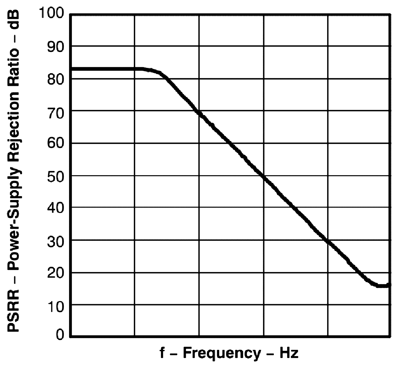
• The graph looks a whole lot like the open loop response graph of an op amp. It does not have anything to do with the open loop response, however. Do not confuse the two!
• The important thing is the power supply rejection gets worse at high frequencies, and these are the frequencies that are likely to get conducted into an op amp from high-speed digital circuitry!
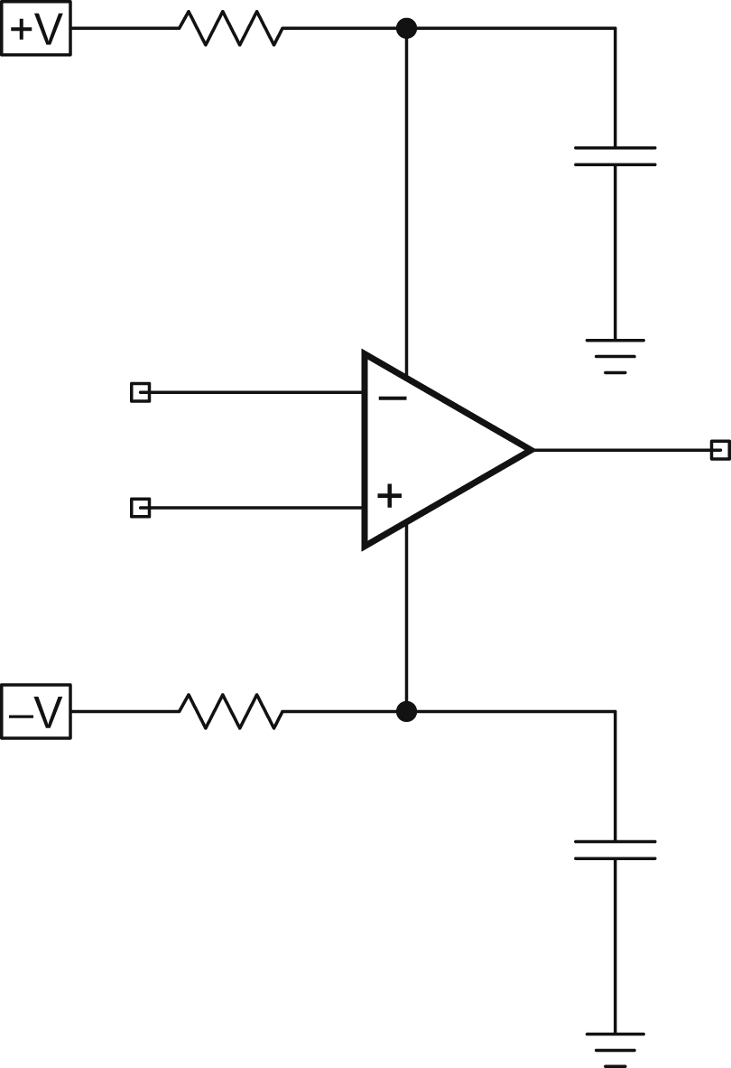
Fortunately, there is a very simple thing you can do to combat this problem. You can place a small series resistor in line with the power supply inputs, and put the decoupling caps after the series resistor as shown in Fig. 13.8.
You have, in effect, made a single-pole low-pass filter on the power input, which will reject the power supply with the same degree of rejection that the PSRR is deteriorating! Before you get too excited, I need to give you some cautions:
• Op Amp supply current, particularly for high-speed op amps, can be above 10 mA. And if you are using an IC with more than one op amp, that current is multiplied by the number of op amps. This will limit your choice of series resistors to just a few Ohms at most. A current-starved op amp will also produce many strange symptoms! Reduce the series resistance if you encounter unusual effects.
• If you place too much series resistance on the power input of the op amp, the supply voltage on its power pins will be reduced. This will reduce the output voltage swing of the op amp. Remember that you can always measure the voltage, and if it is too low, you need to reduce the value of series resistance.
• The decoupling capacitors are now serving double duty as the frequency element in a low-pass filter. If there is more than one capacitor, you add the capacitance. It is seldom necessary to exactly counter the op amp power supply rejection ratio; you only need to achieve a flat response at your bandwidth of interest that is sufficiently high to isolate your circuit from the effects of high frequencies on the board.
• Because you are now effectively designing a single-pole low-pass filter on the power supply, and the capacitor will form the low-pass breakpoint with the series resistor and likely be a relative large value, use a good quality capacitor. If your circuit encounters thermal effects, be aware of the effect of temperature on capacitance value.
• Nothing in this scheme of reducing PSRR negates data sheet requirements for decoupling capacitor (see Appendix B). Your low-pass filter capacitor should be at least the value(s) recommended in the data sheet, and the capacitor should still be located close to the power supply pins of the op amp.
13.7. The Output Has an Offset
This error can appear in both DC and AC circuits. A DC circuit is more difficult to deal with and usually involves selecting a different op amp, or carefully canceling the offset by using an op amp with an “offset null” function. I have not discussed the offset null function of op amps, because it is a feature that is seldom used or necessary. As op amps get better and better, the offset nulling function is being increasingly omitted; however, some older op amps persist in the marketplace due to their popularity, particularly in military applications.
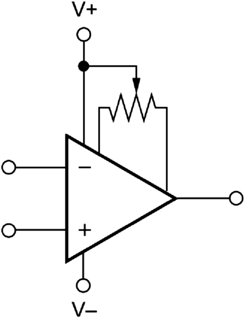
The offset null pins are usually pins 1 and 5 of the standard 8 pin single op amp package, although pin 8 is sometimes used (Fig. 13.9).
The usual method of offset nulling involves a potentiometer between the two pins, and the center adjustment connected to V−, although some op amps connect to V+ instead. Follow the manufacturer's recommendation (Fig. 13.10).

Going back to the previous section—if you need to slow down the slew rate of an op amp with offset null pins—they are direct connections to the long-tail pair emitters! So added a slew rate reduction capacitor to an op amp with offset null function is extremely easy.
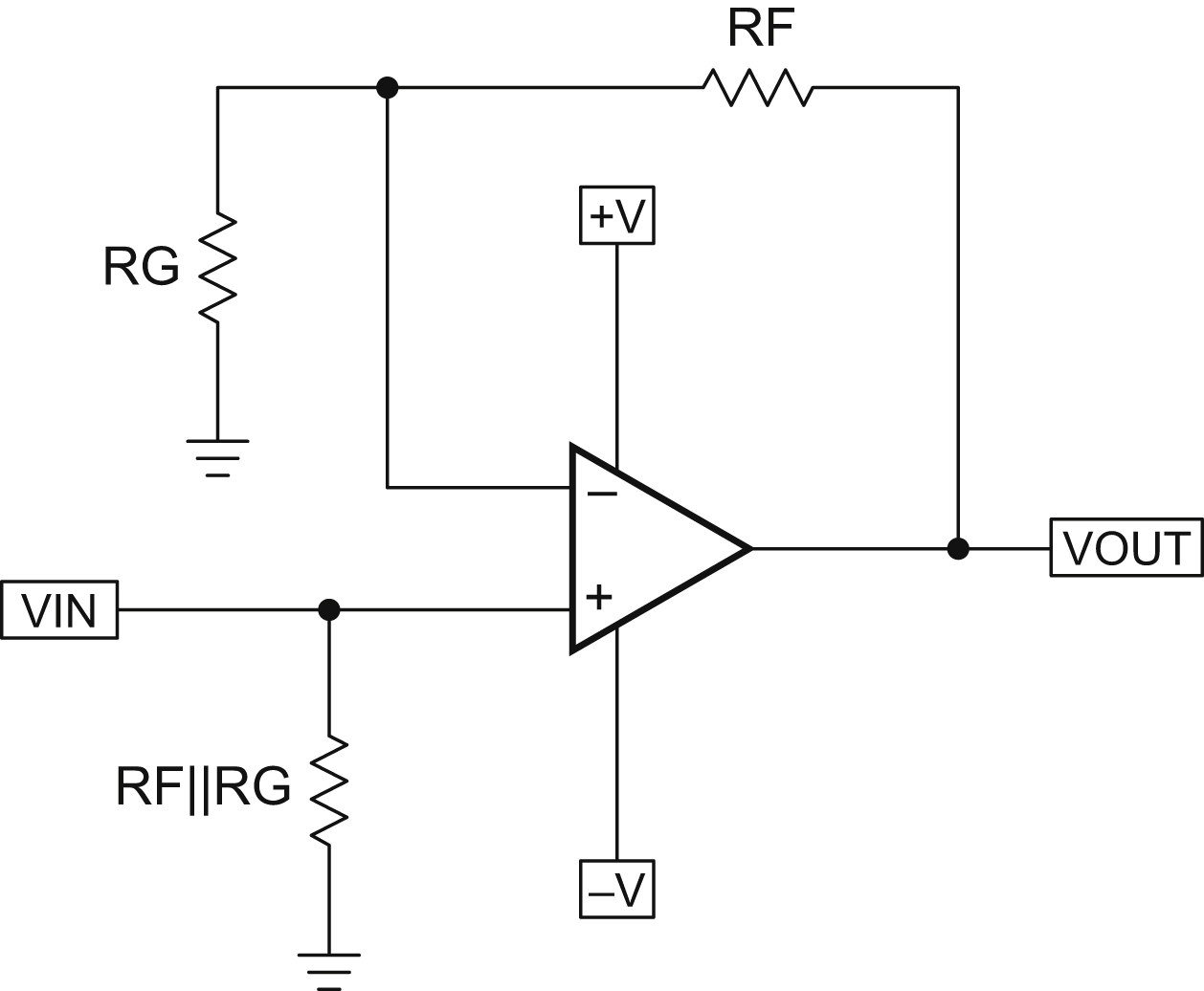
A lot of people get into trouble applying inverting op amp circuits that must include DC gain when they fail to take input bias current into account. All op amp inputs require input bias current, which must be supplied by the user. For the common mode rejection of an op amp to work properly (and reject the DC offset), the input bias currents of the inverting and noninverting inputs must be balanced. The easiest way to do this is with a resistor inserted between the noninverting input and ground (or virtual ground). The value of this resistor is RF∥RG. The reason for this value is intuitive. Replacing the input voltage VIN with ground, the input gain resistor RG is connected to ground. But the output of the op amp in this condition is also at ground potential, so RF is effectively also connected to ground. Therefore, the input bias current of the inverting input is RF∥RG. So if you want to balance the input bias current, the resistor at the noninverting input should also be RF∥RG as shown in Fig. 13.11.
Consider the case of a noninverting gain circuit shown in Fig. 13.12.
You almost certainly selected the noninverting gain configuration because of its high input impedance, but RF∥RG works against that high input impedance, particularly in the case of high gain, high-speed op amp circuits, where RG tends to be small. So most designers choose to omit it and rely on the resistance of VIN to provide input bias. However, that unbalances the input bias current and leads to offset. Fortunately, high-speed application circuits are seldom concerned with DC accuracy. If this is a concern, then you can easily get rid of DC at the output by adding one capacitor as shown in Fig. 13.13.
The DC gain of this circuit is unity, because the added capacitor blocks DC, converting the stage to a unity gain buffer for DC. RF∥RG can be omitted, provided that the source of VIN provides a path for input bias current. If not, it can be made large enough not to load the input, because you no longer have to worry about amplifying DC errors.


13.8. Conclusion
This chapter has given you a basic set of tools to combat some of the common problems that arise in applying op amps. It is by no means comprehensive, I cannot anticipate everything that might go wrong, but I believe this should allow you to rule out the most common mistakes and troublesome annoyances. You might also want to consult Chapter 25—which is a compilation of actual problems reported to me by customers when I was an applications engineer—and their solutions.
..................Content has been hidden....................
You can't read the all page of ebook, please click here login for view all page.