
7
Gate Turn-off Thyristors
Electrical and Computer Engineering, University of West Florida, 11000 University Parkway, Pensacola, Florida 32514-5754, USA
7.1 Introduction
7.2 Basic Structure and Operation
7.4.1 On-state Characteristics
7.4.2 Off-state Characteristics
7.5 Switching Phases
7.6 SPICE GTO Model
7.7 Applications
7.1 Introduction
A gate turn-off thyristor (known as a GTO) is a three terminal power semiconductor device. GTOs belong to a thyristor family having a four-layer structure. GTOs also belong to a group of power semiconductor devices that have the ability for full control of on- and off-states via the control terminal (gate). To fully understand the design, development and operation of the GTO, it is easier to compare with the conventional thyristor. Like a conventional thyristor, applying a positive gate signal to its gate terminal can turn-on to a GTO. Unlike a standard thyristor, a GTO is designed to turn-off by applying a negative gate signal.
GTOs are of two types: asymmetrical and symmetrical. The asymmetrical GTOs are the most common type on the market. This type of GTOs is normally used with a anti-parallel diode and hence high reverse blocking capability is not available. The reverse conducting is accomplished with an anti-parallel diode integrated onto the same silicon wafer. The symmetrical type of GTOs has an equal forward and reverse blocking capability.
7.2 Basic Structure and Operation
The symbol of a GTO is shown in Fig. 7.1a. A high degree of interdigitation is required in GTOs in order to achieve efficient turn-off. The most common design employs the cathode area separated into multiple segments (cathode fingers) arranged in concentric rings around the device center. The internal structure is shown in Fig. 7.1b. A common contact disc pressed against the cathode fingers connects the fingers together. It is important that all the fingers turns off simultaneously, otherwise the current may be concentrated into a fewer fingers which are likely to be damaged due to over heating.
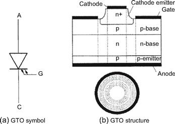
FIGURE 7.1 GTO structure.
The high level of gate interdigitation also results in a fast turn-on speed and a high di/dt performance of the GTOs. The most remote part of a cathode region is not more than 0.16 mm from a gate edge and hence the whole GTO can conduct within about 5 (is with sufficient gate drive and the turn-on losses can be reduced. However, the interdigitation reduces the available emitter area so the low frequency average current rating is less than for a standard thyristor with an equivalent diameter.
The basic structure of a GTO consists of a four-layer-PNPN semiconductor device, which is very similar in construction to a thyristor. It has several design features which allow it to be turned on and off by reversing the polarity of the gate signal. The most important differences are that the GTO has long narrow emitter fingers surrounded by gate electrodes and no cathode shorts.
The turn-on mode is similar to a standard thyristor. The injection of the hole current from the gate forward biases the cathode p-base junction causing electron emission from the cathode. These electrons flow to the anode and induce hole injection by the anode emitter. The injection of holes and electrons into the base regions continues until charge multiplication effects bring the GTO into conduction. This is shown in Fig. 7.2a. As with a conventional thyristor only the area of cathode adjacent to the gate electrode is turned on initially, and the remaining area is brought into conduction by plasma spreading. However, unlike the thyristor, the GTO consists of many narrow cathode elements, heavily interdigitated with the gate electrode, and therefore the initial turned-on area is very large and the time required for plasma spreading is small. The GTO, therefore, is brought into conduction very rapidly and can withstand a high turn-on di/dt.
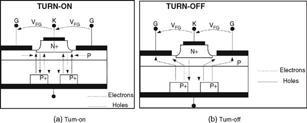
FIGURE 7.2 Turn-on and turn-off of GTOs.
In order to turn-off a GTO, the gate is reversed biased with respect to the cathode and holes from the anode are extracted from the p-base. This is shown in Fig. 7.2b. As a result a voltage drop is developed in the p-base region, which eventually reverse biases the gate cathode junction cutting off the injection of electrons. As the hole extraction continues, the p-base is further depleted, thereby squeezing the remaining conduction area. The anode current then flows through the most remote areas from the gate contacts, forming high current density filaments. This is the most crucial phase of the turn-off process in GTOs, because high density filaments leads to localized heating which can cause device failure unless these filaments are extinguished quickly. An application of higher negative gate voltage may aid in extinguishing the filaments rapidly. However, the breakdown voltage of the gate-cathode junction limits this method.
When the excess carrier concentration is low enough for carrier multiplication to cease, the device reverts to the forward blocking condition. At this point although the cathode current has stopped flowing, anode-to-gate current continues to flow supplied by the carriers from n-base region stored charge. This is observed as a tail current that decays exponentially as the remaining charge concentration is reduced by recombination process. The presence of this tail current with the combination of high GTO off-state voltage produces substantial power losses. During this transition period, the electric field in the n-base region is grossly distorted due to the presence of the charge carriers and may result in premature avalanche breakdown. The resulting impact ionization can cause device failure. This phenomenon is known as “dynamic avalanche.” The device regains its steady-state blocking characteristics when the tail current diminishes to leakage current level.
7.3 GTO Thyristor Models
One-dimensional two-transistor model of GTOs is shown in Fig. 7.3. The device is expected to yield the turn-off gain g given by
![]() (7.1)
(7.1)
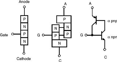
FIGURE 7.3 Two-transistor model representing the GTO thyristor.
where IA is the anode current and IG the gate current at turn-off, and αnpn and apnp are the common-base current gains in the NPN and PNP transistors sections of the device. For a non-shorted device, the charge is drawn from the anode and regenerative action commences, but the device does not latch on (remain on when the gate current is removed) until
![]() (7.2)
(7.2)
This process takes a short period while the current and the current gains increase until they satisfy Eq. (7.2). For anode-shorted devices, the mechanism is similar but the anode short impairs the turn-on process by providing a base–emitter short thus reducing the PNP transistor gain, which is shown in Fig. 7.4. The composite PNP gain of the emitter-shorted structure is given as follows
![]() (7.3)
(7.3)
where Vbe = emitter base voltage (generally 0.6 V for injection of carriers), and Rs is the anode short resistance. The anode emitter injects when the voltage around it exceed 0.06 V, and therefore the collector current of the NPN transistor flowing through the anode shorts influences turn-on.
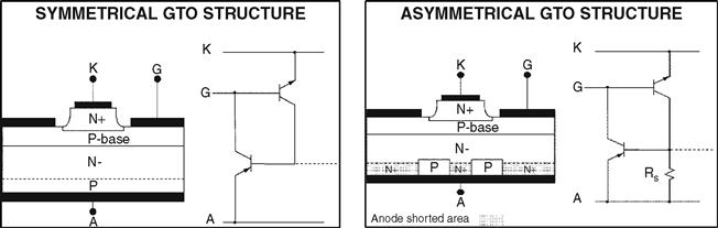
FIGURE 7.4 Two-transistor models of GTO structures.
The GTO remains in a transistor state if the load circuit limits the current through the shorts.
7.4 Static Characteristics
7.4.1 On-state Characteristics
In the on-state the GTO operates in a similar manner to the thyristor. If the anode current remains above the holding current level then positive gate drive may be reduced to zero and the GTO will remain in conduction. However, as a result of the turn-off ability of the GTO, it does posses a higher holding current level than the standard thyristor, and in addition, the cathode of the GTO thyristor is sub-divided into small finger elements to assist turn-off. Thus, if the GTO thyristor anode current transiently dips below the holding current level, localized regions of the device may turn-off, thus forcing a high anode current back into the GTO at a high rate of rise of anode current after this partial turn-off. This situation could be potentially destructive. It is recommended, therefore, that the positive gate drive is not removed during conduction but is held at a value IG(ON), where IG(ON) is greater than the maximum critical trigger current (IGT) over the expected operating temperature range of the GTO thyristor.
Figure 7.5 shows the typical on-state V-I characteristics for a 4000 A, 4500 V GTO from Dynex range of GTOs [1] at junction temperatures of 25°C and 125°C. The curves can be approximated to a straight line of the form
![]() (7.4)
(7.4)
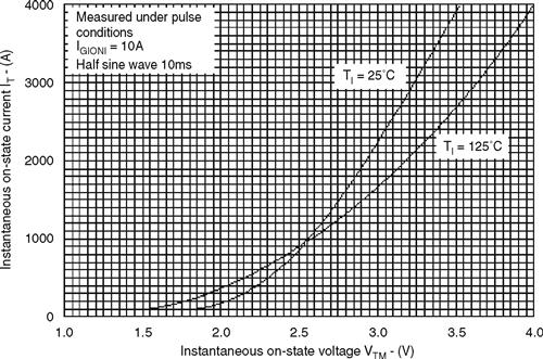
FIGURE 7.5 V-I characteristics of GTO [see data sheet in Ref. 1].
where V0 = voltage intercept, models the voltage across the cathode and anode forward biased junctions and R0 = on state resistance. When average and RMS values of on-state current (ITAV, ITRMS) are known, then the on-state power dissipation PON can be determined using V0 and R0. That is,
![]() (7.5)
(7.5)
7.4.2 Off-state Characteristics
Unlike the standard thyristor, the GTO does not include cathode emitter shorts to prevent non-gated turn-on effects due to dv/dt induced forward biased leakage current. In the off-state of the GTO, steps should, therefore, be taken to prevent such potentially dangerous triggering. This can be accomplished by either connecting the recommended value of resistance between the gate and the cathode (RGK) or by maintaining a small reverse bias on the gate contact (VRG = − 2V). This will prevent the cathode emitter becoming forward biased and therefore sustain the GTO thyristor in the off state.
The peak off-state voltage is a function of resistance RGK. This is shown in Fig. 7.6. Under ordinary operating conditions, GTOs are biased with a negative gate voltage of around − 15 V supplied from the gate drive unit during the off-state interval. Nevertheless, provision of RGK maybe desirable design practice in the event of the gate-drive failure for any reason (RGK < 1.5 Ω is recommended for a large GTO). RGK dissipates energy and hence adds to the system losses.
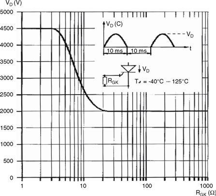
FIGURE 7.6 GTO blocking voltage vs. RGK [see data sheet in Ref. 1].
7.4.3 Rate of Rise of Off-state Voltage [dvT/dt)
The rate of rise of off-state voltage (dvr/dt) depends on the resistance RGK connected between the gate and the cathode and the reverse bias applied between the gate and the cathode. This relationship is shown in Fig. 7.7.
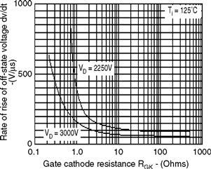
FIGURE 7.7 dVD/dt vs. RGK [see data sheet in Ref. 1].
7.4.4 Gate Triggering Characteristics
The gate trigger current (IGT) and the gate trigger voltage (VGT) are both dependent on junction temperature Tj as shown in Fig. 7.8. During the conduction state of the GTO a certain value of gate current must be supplied and this value should be larger than the IGT at the lowest junction temperature at which the GTO operates. In dynamic conditions the specified IGT is not sufficient to trigger the GTO switching from higher voltage and high di/dt. In practice a much high peak gate current IGM (in order of ten times IGT) at Tj min is recommended to obtain good turn-on performance.
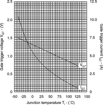
FIGURE 7.8 GTO trigger characteristics [see data sheet in Ref. 1].
7.5 Switching Phases
The switching process of a GTO thyristor goes through four operating phases (a) turn-on, (b) on-state, (c) turn-off, and (d) off-state.
Turn-on: A GTO has a highly interdigited gate structure with no regenerative gate. Thus it requires a large initial gate trigger pulse. A typical turn-on gate pulse and its important parameters are shown in Fig. 7.9. A minimum and maximum values of IGM can be derived from the device data sheet. A value of dig/dt is given in device characteristics of the data sheet, against turn-on time. The rate of rise of gate current, dig/dt will affect the device turn-on losses. The duration of the IGM pulse should not be less than half the minimum on time given in data sheet ratings. A longer period will be required if the anode current di/dt is low such that IGM is maintained until a sufficient level of anode current is established.

FIGURE 7.9 A typical turn-on gate pulse [see data sheet in Ref. 2].
On-state: Once the GTO is turned on, forward gate current must be continued for the whole of the conduction period. Otherwise, the device will not remain in conduction during the on-state period. If large negative di/dt or anode current reversal occurs in the circuit during the on-state, then higher values of IG may be required. Much lower values of IG are, however, required when the device has heated up.
Turn-off: The turn-off performance of a GTO is greatly influenced by the characteristics of the gate turn-off circuit. Thus the characteristics of the turn-off circuit must match with the device requirements. Figure 7.10 shows the typical anode and gate currents during the turn-off. The gate turn-off process involves the extraction of the gate charge, the gate avalanche period and the anode current decay. The amount of the charge extraction is a device parameter and its value is not significantly affected by the external circuit conditions. The initial peak turn-off current and turn-off time, which are important parameters of the turning-off process, depend on the external circuit components. The device data sheet gives typical values for IGQ.
FIGURE 7.10 Anode and gate currents during turn-off [see data sheet in Ref. 2].
The turn-off circuit arrangement of a GTO is shown in Fig. 7.11. The turn-off current gain of a GTO is low, typically 6-15. Thus, for a GTO with a turn-off gain of 10, it will require a turn-off gate current of 10 A to turn-off an on-state of 100 A. A charged capacitor C is normally used to provide the required turn-off gate current. Inductor L limits the turn-off di/dt of the gate current through the circuit formed by R1, R2, SW1, and L. The gate circuit supply voltage VGS should be selected to give the required value of VGQ. The values of R1 and R2 should also be minimized.

FIGURE 7.11 Turn-off circuit [see data sheet in Ref. 2].
Off-state period: During the off-state period, which begins after the fall of the tail current to zero, the gate should ideally remain reverse biased. This reverse bias ensures maximum blocking capability and dv/dt rejection. The reverse bias can be obtained either by keeping SW1 closed during the whole off-state period or via a higher impedance circuit SW2 and R3 provided a minimum negative voltage exits. This higher impedance circuit SW2 and R3 must sink the gate leakage current.
In case of a failure of the auxiliary supplies for the gate turn-off circuit, the gate may be in reverses biased condition and the GTO may not be able to block the voltage. To ensure blocking voltage of the device is maintained, then a minimum gate-cathode resistance (RGK) should be applied as shown in Fig. 7.12. The value of RGK for a given line voltage can be derived from the data sheet.

FIGURE 7.12 Gate-cathode resistance, RGK [see data sheet in Ref. 2].
7.6 SPICE GTO Model
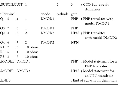
A GTO maybe modelled with two transistors shown in Fig. 7.3. However, a GTO model [3] consisting of two thyristors, which are connected in parallel, yield improved on-state, turn-on, and turn-off characteristics. This is shown in Fig. 7.13 with four transistors.
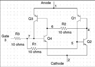
FIGURE 7.13 Four-transistor GTO model.
When the anode to cathode voltage, VAK is positive and there is no gate voltage, the GTO model will be in the off-state like a standard thyristor. If a positive voltage (VAK) is applied to the anode with respect to the cathode and no gate pulse applied, IB1 = IB 2 = 0 and therefore IC1 = IC2 = 0. Thus no anode current will flow, IA = IK = 0.
When a small voltage is applied to the gate, then JB2 is nonzero and therefore both IC1 = IC2 = 0 are non-zero. Thus the internal circuit will conduct and there will a current flow from the anode to the cathode.
When a negative gate pulse is applied to the GTO model, the PNP junction near to the cathode will behave as a diode. The diode will be reverse biased since the gate voltage is negative with to the cathode. Therefore the GTO will stop conduction.
When the anode-to-cathode voltage is negative, that is, the anode voltage is negative with respect to the cathode, the GTO model will act like a reverse biased diode. This is because the PNP transistor will see a negative voltage at the emitter and the NPN transistor will see a positive voltage at the emitter. Therefore both transistors will be in the off-state and hence the GTO will not conduct. The SPICE sub-circuit description of the GTO model will be as follows
7.7 Applications
GTO thyristors find many applications such as in motor drives, induction heating [4], distribution lines [5], pulsed power [6], and Flexible AC transmission systems [7, 8].
REFERENCES
1. Dynex semiconductor: Data GTO data-sheets web-site: http://www.dynexsemi.com/products/power_search.cgi.
2. Westcode semiconductor: Data GTO data-sheets web-site: http://www.westcode.com/ws-gto.html.
3. El-Amin IMA. GTO PSPICE Model and its applications. The Fourth Saudi Engineering Conference. November 1995; vol. III:271–277.
4. Busatto G, Iannuzzo F, Fratelli L. PSPICE model for GTOs. Proceedings of Symposium on Power Electronics Electrical Drives. Advanced Machine Power Quality. 3–5 June 1998; vol. 1:2/5–210.
5. Malesani L, Tenti P. Medium-frequency GTO inverter for induction heating applications. Second European Conference on Power Electronics and Applications. 22–24, September 1987; vol. 1:271–276.
6. Souza LFW, Watanabe EH, Aredes MA. GTO controlled series capacitor for distribution lines. International Conference on Large High Voltage Electric Systems. 1998.
7. Chamund DJ. Characterisation of 3.3 kV asymmetrical thyristor for pulsed power application. IEE Symposium Pulsed Power 2000. May 2000; 3–4.
8. Moore P, Ashmole P. Flexible AC transmission systems: 4. Advanced FACTS controllers. Power Engineering Journal. April 1998; vol. 12(no. 2):95–100.