
26
Solid State Pulsed Power Electronics
Instituto Superior de Engenharia de Lisboa, DEEA, and Nuclear Physics Center fom Lisbon University, Av. Prof. Gama Pinto 2, 1649-003 Lisboa, Portugal
TU Lisbon, Instituto Superior Técnico, DEEC, A.C. Energia, Center for Innovation on Electrical and Energy Engineering, AV. Rovisco Pais 1, 1049–001 Lisboa, Portugal
26.1 Introduction
26.2 Power Semiconductors for Pulsed Power
26.2.1 High-Voltage PIN Diodes (SOS Diodes)
26.2.2 Metal Oxide Semiconductor Technology Transistors
26.2.3 Thyristors and Turn-Off Thyristor Devices
26.2.4 Power JFETs and Derived Devices
26.2.5 Semiconductor Series Stacks and Generalized Cascodes, Semiconductor Parallel Stacks
26.3 Load Types and Requirements
26.4 Solid-State Pulsed Power Topologies
26.4.1 Direct Switching
26.4.2 DC–DC Isolated Converters
26.4.3 Cascade Circuits
26.4.4 Solid-State Marx Generators
26.1 Introduction
Pulsed power (PP) can be considered as the science and technology of accumulating electrical energy over a relatively long period of time followed by the subsequent energy release in very short pulses, a single one or a controlled repetitive sequence, thus increasing the instantaneous peak power. An example is shown in Fig. 26.1, where a stored energy of 1 kJ can be discharged into a long pulse of 1 kW for 1 s or a short pulse of 1 GW for 1 µs, respectively, considering the ideal case of a lossless system.
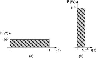
FIGURE 26.1 Discharge of 1 kJ energy; (a) 1 kW during 1s pulse, (b) 1 GW during 1 µs pulse.
Pulsed power is a technique primarily developed for radars, accelerators, and military applications, but with the potential for civil applications [1]. In fact, there is a growing variety of environmental, biomedical, commercial, and industrial applications that use positive and/or negative high-voltage (HV) repetitive pulses for enhancing the properties of a product or a technique [2]. These pulses may last anywhere from hundreds of picoseconds to tens of seconds, being released as a single shot or as a repetitive sequence up to several tens of thousands per second.
What makes PP so unique is the concept that one can deliver extremely high peak powers during short times without the demand for highly powerful energetic power sources, used in custom direct (dc) or alternating (ac) voltage systems.
Previously, this technology was dominated by vacuum or gas tubes (i.e., electronic valves) for switching the high powers needed for military and large plant physical applications [3]. With the technological advent of power semiconductors in the seventies and particularly modern power semiconductors in the nineties, it was possible to develop PP generators based on power semiconductors, still, lower power rated compared with the electronic valves, but largely rewarded by the higher energetic efficiency and flexibility together with compactness and cost effectiveness [4].
Nowadays, the applications of PP are driving the need for technological advances in medical, environment, biological, energetic and industrial applications. For example, in the reduction of pollution emissions from fossil fuels, in killing bacteria and organic pollutants, in melanoma cancer treatment, in molding metals sheets, and so on [5–9].
This chapter provides basic concepts and advanced know-how on the generation of repetitive HV pulses using state of the art power semiconductor technology. Apart from this introduction, in Section 26.2, “Power Semiconductors for Pulsed Power,” the most common power semiconductors devices used in solid-state-based high-voltage generators are reviewed. In Section 26.3, “Load Types and Requirements,” several types of pulsed power applications are presented, and the type of load requirements they present to the high-voltage modulators are described. The most widespread semiconductor-based HV pulse modulator topologies are analyzed and discussed in terms of solid-state devices operation in Section 26.4, “Solid-State Pulsed Power topologies.” Finally, the main conclusions about semiconductors use in high-voltage pulse generation are presented and the future trends on this technology are discussed in Section 26.5, “Conclusions and Future Trends.”
26.2 Power Semiconductors for Pulsed Power
The demand for high-voltage modulators to generate repetitive high-voltage pulses with optimized performance and characteristics, based in solid-state technology, still needs enhancement of the Volt–Ampere capabilities and switching speed of modern power semiconductors.
Therefore, using power semiconductors in pulsed power is a matter of optimizing their use, going beyond the present semiconductor ratings and taking advantage of usually nonuseful phenomena or nonideal characteristics, such as controlled avalanche breakdown (for avalanche transistors), diode reverse recovery sharpness that can generate inductive high-voltage pulses, Zener capacitances, peak currents, and unusual very short-pulse behavior.
In the following subsections, the particular characteristics of power semiconductors enabling their use in pulsed power applications will be summarized, from the high-voltage diode through the latest silicon carbide (SiC) power junction field-effect transistors. To overcome power semiconductor’s limited hold-off voltage and current ratings (Fig. 26.2), some techniques will be described, including series and parallel semiconductor arrangements, up to the cascode stacks.
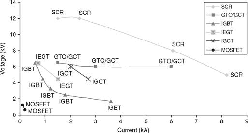
FIGURE 26.2 Current maximum Volt–Ampere capabilities of high-power semiconductors (SCR, silicon-controlled rectifier; GTO, gate turn-off thyristor; GCT, gate-controlled thyristor; IGCT, integrated gate-commutated thyristor; IEGT, injection-enhanced gate transistor; IGBT, insulated gate bipolar transistor; MOSFET, metal-oxide semiconductor field-effect transistors).
26.2.1 High-Voltage PIN Diodes (SOS Diodes)
Figure 26.3a shows the simplified structure of a typical high-voltage, high-power diode with forward-bias carriers [10]. It has a heavily doped P+ anode and N+ substrate on which a lightly doped N− (or near intrinsic, I) epitaxial layer, called drift region, is formed [11]. The drift region, usually not found in low-power diodes, has to contain the depletion layer of the reverse-biased high-voltage PIN diode, establishing the diode reverse breakdown (or hold-off) voltage rating (punch-through diodes).
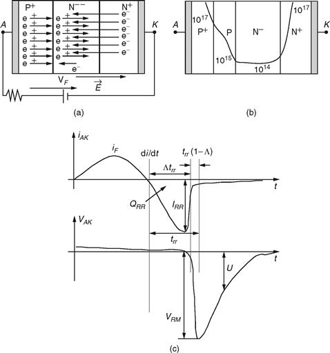
FIGURE 26.3 (a) Forward-biased PIN diode; (b) P+PN− N+ SOS diode structure and typical doping profile; and (c) SOS diode reverse blocking behavior.
PIN diodes turn-on requires removal of the depletion layer (the diode is reverse biased prior to turn-on). Removal of the stored depletion charge needs a certain current and time. Forward conduction is dominated by injected holes (conductivity modulation) in the drift region, which becomes a virtual P region. The minority injected charge is positive if the diode is conducting, the forward current providing minority carriers at the rate they recombine.
To turn-off the PIN diode, the stored excess carriers, mostly in the drift region, must be discharged before the diode reverse biases, the minority charge becoming negative. Upon applying a reverse voltage UR, the forward current will decrease at a rate of di/dt ≈ IRR/trr, (Fig. 26.3c), becoming negative to swept the excess carriers out of the drift region and charge the depletion capacitance Ceqoff. At constant UR voltage applied in inductive circuits (LS inductor), the diode reverse current rate is di/dt ≈ UR/LS, reaching the value IRR = trrUR/Ls at the reverse recovery time trr = LsIrr/Ur, being the reverse recovery charge QRR = IRRtrr/2.
In LC oscillating circuits (Fig. 26.4), the PIN diode may become reverse biased by a negative fast rising voltage with high peak value Vrm, which can be more than three times higher than the applied direct voltage U (Fig. 26.3c).
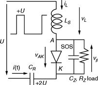
FIGURE 26.4 SOS pulse generation using magnetic energy storage.
At high reverse voltages, the pulse energy must be limited to avoid the impact ionization current to destroy the diode by avalanche breakdown and excessive power dissipation. Therefore, PIN diodes should be used with very short pulses, sharpening and increasing the voltage amplitude of the applied pulses.
Semiconductor Opening Switches (SOS) are modified PIN high-voltage diodes using a P+PN−N+ structure with gradual doped P layer (Fig. 26.3b) [12]. They are optimized to exhibit relatively slow reverse recovery (∧ tRR ≈ 50–100 ns) but abrupt recovery (very fast reverse current decay) (1 − ∧)trr ≈ 5 ns (Fig. 26.3c).
SOS characteristics depend not only on the pumping forward current (current density and very short time to avoid saturation) but also on the doping profile of the P+PN−N+ structure. The reverse recovery of SOS diodes (e.g., their opening) should differ from PIN diodes, since current interruption ought to occur mostly in the narrower P doped layer, not in the drift layer. The SOS can switch high currents (kA) in nanosecond opening times, with automatic uniform distribution of reverse voltage (kV) in series-connected SOSs during current decay. Series stacks of up to 1000 SOSs can be deployed to obtain working voltages near the megavolt level, peak currents of several kiloampere, peak power of gigawatts, and average powers of tens of kilowatts.
In a simplified circuit for SOS operation (Fig. 26.4), it is supposed that a rectangular prepulse with amplitude U and pulse length TU is generated and applied to the SOS in series with an inductor LS to charge the capacitor CR.
During the positive part of the prepulse, the forward pumping period, the SOS diode is forward biased, and the inductor sinusoidal current rises to build up energy in the resonant LsCr circuit and excess carriers in the diode, the capacitor Cr being charged to nearly 2U. Neglecting losses, parasitic effects, and diode voltage drops, the peak forward current is IF ≈ U/Zr, where ![]() is the characteristic impedance of the LsCr resonant tank with oscillation frequency
is the characteristic impedance of the LsCr resonant tank with oscillation frequency ![]() . Charging only occurs during the pulse length TU. Neglecting the recombination decay time constant, the diode forward stored charge is nearly 2IF/ωR.
. Charging only occurs during the pulse length TU. Neglecting the recombination decay time constant, the diode forward stored charge is nearly 2IF/ωR.
During the sinusoidal negative oscillation interval, the prepulse voltage is nearly zero and the inductor current goes negative. The SOS diode opens at nearly the Cr discharge peak current Irr≈ 2U/Zr ≈ 2IF, being the reverse recovery charge QRR≈ IRR/ωR nearly equal to the forward injected charge.
Supposing diode abrupt recovery and assuming energy conservation, the maximum vp pulse voltage Vrm is dependent on the load capacitor Cz and resistor RZ, being ≈ for ![]() Cz, where RZ is paralleled with
Cz, where RZ is paralleled with ![]() , the characteristic impedance of the second-order LsCz circuit with damping factor τ and natural frequency
, the characteristic impedance of the second-order LsCz circuit with damping factor τ and natural frequency ![]() .
.
For near optimum energy transfer, damping slightly lower than the critical value should be used, the vp pulse being roughly sinusoidal. Pulse forming networks or lines can be used to almost square it [12].
To obtain a near critical damped load (0.7< τ < 1), it must be 1.4 Rz < Zz < 2Rz. Then, from the required Vrm and Irr, the ZR value, it is ![]() , being LS ≈ ZR/ωR and CR ≈ 1/(ZRωR). From Ls and Zz, the load parallel capacitor Cz, either added or stray capacitance or SOS Ceqoff, should be CZ ≈LS/Z2Z.
, being LS ≈ ZR/ωR and CR ≈ 1/(ZRωR). From Ls and Zz, the load parallel capacitor Cz, either added or stray capacitance or SOS Ceqoff, should be CZ ≈LS/Z2Z.
For a required VRM in load resistor Rz and capacitor CZ, the SOS diode must withstand the forward current IF, pumping time TU, reverse voltage VRM, reverse recovery current IRR, and reverse recovery charge QRR.
High peak voltages Vrm and comparatively low values of Irr need very low values of the load (spurious) parallel capacitance Cz or higher values of IRR.
EXAMPLE 26.1 Determine the circuit parameters of Fig. 26.4 to obtain a 30 ns 1MV pulse in resistor Rz = 1kω (1 MW peak) paralleled with Cz capacitor, from a prepulse having U = 300 kV and pulse length TU.
SOLUTION. The prepulse length should be TU ≈ 30 × 10− 9 × 10⁶/(300 × 103)≈ 100 ns. Then, from the above equations, it is obtained ωR=π/TU =π/(100 × 10− 9)≈ 3.14 × 10⁷, ZZ≈ 1.5RZ≈ 1.5 kω, RZ||ZZ ≈ 600ω, ZR ≈ 2U(RZ||ZZ)/VRM ≈ 2× 300× 103× 600/106 ≈ 360ω, LS ≈ ZR/ωR ≈ 360/3.14× 107 ≈ 11.4μH, CR ≈ 1/(ZRωR) ≈ 1/(360 × 3.14 × 107)≈ 88 pF, and CZ ≈ LS/Z2 Z ≈ 11.4 × 10− 6/3602≈ 5.1 pF, which is a low value, considering stray capacitances, not to forget the SOS diode (or diode association) equivalent off-depletion capacitance Ceqoff. The SOS must withstand IF ≈ U/ZR ≈ 300 × 103/360≈ 833 A, IRR ≈ 2IF ≈ 1.67 kA, VRM ≈ IRR(RZ||ZZ) ≈ 1667 × 600≈ 106 V, QRR ≈ IRR/ωR≈ 1667/3.14 × 107 ≈ 53μC, mean excess carrier (holes) lifetime (reciprocal of recombination decay) higher than 1 μs, and reverse recovery time ![]() ns, nearly half of the forward pumping time.
ns, nearly half of the forward pumping time.
The pulse duration (settling time) is close to ![]() ns, being near the required 30 ns. Closer approximations for higher Cz values require damping factors ξ toward 0.5, which increase SOS diode ratings (IF, IRR, and QRR), but allow the doubling of Cz capacitances.
ns, being near the required 30 ns. Closer approximations for higher Cz values require damping factors ξ toward 0.5, which increase SOS diode ratings (IF, IRR, and QRR), but allow the doubling of Cz capacitances.
This SOS pulse generator multiplies the incoming prepulse amplitude by a factor slightly higher than three. Given the present capabilities of SOS diodes (nearly 1 kA and 1 kV), this 1 MV pulse modulator would require an array of some thousands SOS diodes arranged in series of few paralleled diodes. Oil isolation and cooling, complemented with water/air, are mandatory. Special care must be given to parasitic inductances and capacitances.
Other SOS devices use unique diffusion techniques to achieve ultrafast switching times, such as the Drift Step Recovery Device (DSRD), the Inverse Recovery Diode (IRD), and the Delayed Ionization Devices (DID). Each device is capable of producing pulses ranging from 1 to 10 kV, with rise times between 100 ps and 1 ns.
The PIN diode-based Silicon Avalanche Sharpener (SAS) is a sharpening device that shortens the pulse rise time. It works normally reverse biased, a slow rise time, and short reverse pulse being applied to the SAS in order to avalanche it. When avalanche breakdown of the SAS drift layer occurs, a very short rise time pulse is applied to the load. Avalanche breakdown does not destroy the SAS if the input pulse is short enough.
26.2.2 Metal Oxide Semiconductor Technology Transistors
26.2.2.1 Metal-Oxide Semiconductor Field-Effect Transistors (MOSFET)
MOSFETs are very fast unipolar-carrier enhancement-mode semiconductor devices controlled by the vGs voltage applied at the gate-source terminals (Fig. 26.5a) [10, 11, 13]. Their speed is mostly due to the absence of carrier recombination since in N-type MOSFETs, the carriers are almost only electrons. MOSFET semiconductor structure forms a N+N−PN+ shorted base-emitter bipolar transistor (Fig. 26.5a), which is often referred as behaving as an intrinsic antiparallel PIN diode (Fig. 26.5b).
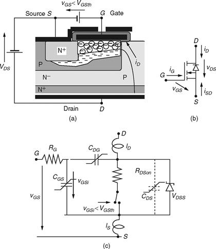
FIGURE 26.5 (a) MOSFET structure showing the Drain-Source current path; (b) Electronic symbol including intrinsic diode; and (c) MOSFET model with parasitic components.
The MOSFET has the capabilities for high-speed switching in the nanosecond or subnanosecond range [14, 15].
In pulsed power applications, MOSFETs should behave as ideal switches, being switched-on if vGs exceeds the threshold value VGSth, vGS > VGSth + VDSon, with VDSon ≈ The ON MOSFET behaves almost like a resistor RDSon with low value and positive temperature coefficient. The MOSFET opens (OFF state, ID ≈ 0) if vGs < VGsth, but usually the gate driver enforces vGs < 0 with vDs > 0. If vDs < 0, then the intrinsic diode starts to conduct (the on voltage is VPINon), which is seldom advantageous since the internal PIN diode is usually not optimized for low voltage drop or high-speed switching. In this case, it is better that the gate driver turns on the MOSFET channel in order to prevent the PIN diode conduction, if − RDSonID < VPINon.
The gate current after charging or discharging of gate stray capacitances is almost null, and therefore, needed gate power is very low. In pulsed power applications, fast switching is needed, therefore the circuits that drive the vGs voltage must charge/discharge the MOSFET parasitic nonlinear capacitances considering the effects of device terminal inductances (Fig. 26.5c). The switching speed of existing MOSFETs is limited mainly by packaging (lead inductances) and drain, gate and source resistances together with intrinsic capacitances.
The switching times can be in the order of some nanoseconds or lower and are affected by the driver RG value. Resistor RG dampens the RLC series circuit that contains CGs, CDG, gate and source stray inductances LS. The gate resistor can be sized adopting a suitable value for the damping factor of the RLC series circuit τ = RG/(2ZG), where ![]() , where CG is the equivalent gate capacitor, being
, where CG is the equivalent gate capacitor, being ![]() .
.
The equivalent gate capacitor CG, can be known from the manufacturers datasheets (CGs = Ciss –Crss; Cdg = Crss; and Cds = Coss –Crss), giving CG ≈ CGS + CDG(dvGS/dvGS), while the gate and source stray inductances LS can be estimated considering typical per unit values. For printed circuit boards (strip lines) or typical parallel wires, inductance LS is usually given nearly by 10nH/cm times the current path total length in centimeters (typical TO220 package of MOSFETs exhibits source terminal inductances of lS ≈ 5 nH). For twisted wire pairs or other low-inductance connections, the value can be lowered down to 3nH/cm. The inductor estimation (and CG nonlinear capacitor calculation) does not need to be very precise since they only affect RG by their square root values.
EXAMPLE 26.2 Calculate the gate resistor for a MOSFET with Cgs ≈ 800 pF and Cdg ≈ 40 pF, operating at a drain voltage of 800 V, driven by vGS = 15 V through a printed circuit strip-line of 5 cm total length.
SOLUTION. For the given strip-line length, it is obtained LS ≈ 50 nH. The gate capacitor is CG ≈ CGS+CDG(dvGD/dvGS)≈ 10− 12 × [800 + 40 × (800/15)]≈ 2.9 nF. Therefore, the gate resistor is ![]() . As CGS and Cdg are nonlinear voltage-dependent capacitances, using RG << Zg can establish gate-source overvoltages two to three times the applied vGS voltage, which can disrupt the gate insulation oxide if they exceed the breakdown voltage Vgss, destroying the MOSFET. To minimize the RG value, for faster gate capacitor charging and switching, it is essential to strongly reduce the stray inductances (if LS ≈ 0, then RG ≈ 0).
. As CGS and Cdg are nonlinear voltage-dependent capacitances, using RG << Zg can establish gate-source overvoltages two to three times the applied vGS voltage, which can disrupt the gate insulation oxide if they exceed the breakdown voltage Vgss, destroying the MOSFET. To minimize the RG value, for faster gate capacitor charging and switching, it is essential to strongly reduce the stray inductances (if LS ≈ 0, then RG ≈ 0).
Fast MOSFET drivers require low stray inductances and often must be based on avalanche transistors [12] (switching bipolar transistors optimized to operate near their collector emitter breakdown voltage VB, but at limited current) or resonant circuits [13]. The avalanche transistors rapidly charge the capacitors CGs and CDG, by transferring capacitor charge from a capacitor reservoir Ca to Cgs and Cdg (Fig. 26.6a). Supposing charge continuity, the MOSFET gate voltage should be VGS ≈ VBCa/(Ca + CG). The Zener diode Z18V helps protect the gate oxide against disruption, but the Zener junction capacitance should be added to the above CG value.
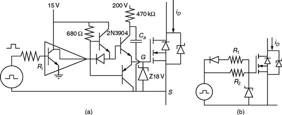
FIGURE 26.6 (a) Avalanche transistor MOSFET driver; (b) Tailoring switching speed using two resistors.
MOSFET switching behavior includes crossing the saturation zone (MOSFET active zone) where iD ≈ K(vGS –VGSth)2 being K, a MOSFET structural parameter (see Chapter 4, “MOSFET,” in this book). This effect can be worsened when switching pulsed power capacitive loads.
Switch-on ton and Switch-off toff times can be tailored using different resistive paths to turn-on (R2) and to turn-off (R1||R2) (Fig. 26.6b) limiting the charging current and the drain voltage rise or fall rates, at the expense of increased switching losses.
Considering the on and off switching times (ton, toff), the dissipated switching power at the switching frequency fs is PS = [(ton + toff) VDSID + CDSV2DS]fs/2.
Pulsed power applications often need semiconductor switch protection to limit load short-circuit current. Since in MOSFETs VDSon ≈ RDSonID, and if RDSon is fairly constant, then short-circuit protection circuits can be based on the measured VDSon voltage (Fig. 26.7a) [10]. Sensed by diode Db3, this voltage, if low enough, maintains the Cz voltage low preventing Dz to avalanche and maintaining Qt2 off. However, if VDSon rises, then Db3 turns off, Cz voltage rises, and Dz avalanches turning Qt2 into saturation that shorts the vGS voltage and turns off the MOSFET. Capacitor Cz acts as a memory, creating a delay that enables the MOSFET turn-on. Figures 26.7b,c show alternatives in which the rate of the vGS decay is slowed to lower the rate of rise of the vDS preventing this voltage to exceed the MOSFET hold-off (avalanche) voltage Vdss. Figure 26.7b shows a capacitive method in which Cg ![]() CG, whereas in Fig. 26.7c, the low-power P MOSFET Mp, in series with the main MOSFET gate, is turned off, putting the high-valued resistor Rg2 in the turn-off path to limit the vGS decay and vDS rate of rise.
CG, whereas in Fig. 26.7c, the low-power P MOSFET Mp, in series with the main MOSFET gate, is turned off, putting the high-valued resistor Rg2 in the turn-off path to limit the vGS decay and vDS rate of rise.
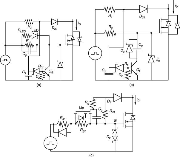
FIGURE 26.7 (a) Active protection against load short circuits; (b) Active protection including capacitive vDS rate limiter; (c) Active protection including resistive vDS rate limiter.
The maximum turn-off overvoltage can also be limited either by using MOSFET parallel connected Zeners (or voltage clamping Metal Oxide Varistors [MOV]) or by using an avalanche diode (with avalanche voltage higher than the supply voltage but somewhat lower than maximum semiconductor voltage rating) in series with a blocking diode connected to the gate-drain terminals (Fig. 26.8).
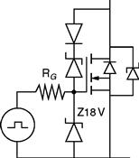
FIGURE 26.8 MOSFET overvoltage protection circuit.
26.2.2.2 Insulated Gate Bipolar Transistors (IGBT)
IGBTs are MOS technology based semiconductor devices, which reduce on-state voltage drop, by adding an extra P+ semiconductor layer in the drain side (Punch-Through IGBT) or by substituting the N+ by a P+ layer (NonPunch-Through [NPT] or Reverse-Blocking IGBT [RB-IGBT]) [10, 11, 13]. The P+ layer injects holes in the drift layer reducing voltage drop by conductivity modulation. The resulting device can be viewed as a low gain high-voltage PNP bipolar transistor driven by a power MOSFET (Fig. 26.9). Gate drivers for IGBTs are similar to those of MOSFETs.
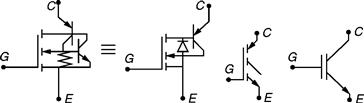
FIGURE 26.9 IGBT equivalent circuit and common symbols.
IGBTs can turn-on almost as fast as MOSFETs, using vGE > VGEth. The on-state saturation voltage VCEsat depends on the vge value and increases rapidly for vge < 12 V, the device risks working into the active zone for lower vge values.
Due to the injected minority recombination into the base, IGBTs are relatively slow turned-off devices and exhibit tail currents. However, they can withstand much higher hold-off voltages (up to 6.5 kV) and currents (up to 3 kA) than MOSFETs, which are limited to nearly 1.2 kV, 100 A peak current. At 6 kV voltages and 3 kA currents, IGBTs on-state losses are significant, degrading efficiency and causing heat removal problems, yet they are being used in very high-voltage systems [16–19].
Most considerations about the MOSFET drive and protections are still valid for IGBTs. In particular, in shoot-through situations, the IGBT device can be protected by detecting desaturation voltage, then shutting down the IGBT using gate-drive circuits similar to those in Fig. 26.7.
26.2.2.3 Injection-Enhanced Gate Transistors (IEGT)
IEGT are IGBT-like structures with deep trench-gates and wider cell widths. Hole concentration in the P layer under the gate electrode is enhanced due to hole accumulation, similar to the conductivity modulation of a PIN diode, lowering the on-state voltage and increasing the efficiency specially in high-voltage devices. The enhanced carrier distribution under the gate electrode leads to higher conductivity of the N-base region in the trench-gate IGBT structure, as the gate region extends into the N-base region below the P-base layer. This phenomenon has been called the injection enhancement effect in deep trench-gate IGBT structures and enables higher device voltage rating. As this phenomenon of carrier enhancement under the gate electrode occurs in all IGBT structures, including the planar-gate structures, the IEGT device is a kind of IGBT and can be viewed as such, although their particular physical structure enables them to withstand higher voltages and currents than planar IGBTs structures. The same is valid for similar proposed structures such as the Carrier-Stored Trench-gate Bipolar Transistor (CSTBT-IGBT).
26.2.3 Thyristors and Turn-Off Thyristor Devices
High-voltage high-power thyristors, also termed Silicon Controlled Rectifiers (SCR), are PNIPN structures (Fig. 26.10a) that can be gated-on by injecting a relatively small gate current into the device. In pulsed power applications, thyristors can be used in capacitor discharging circuits, since they can be easily turned on by a small gate current [10, 11, 13]. Thyristor turn-off behavior is not gate-controlled, being similar to the PIN diode and of little use in pulsed power.
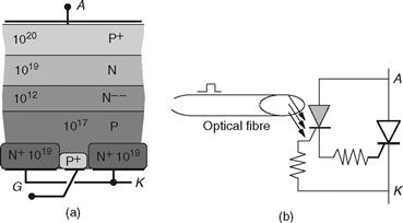
FIGURE 26.10 (a) High-voltage thyristor structure; (b) LTT operating principle.
Thyristors can block voltages near 12 kV (the silicon limit is near 15 kV) and conduct currents up to 8 kA.
Modern thyristor structures like the Light Activated Silicon Controlled Rectifier (LASCR) or the Light-Triggered Thyristors (LTT) are optically triggered (Fig. 26.10b) using an optical fibre and can be valuable in high-voltage applications to enable reducing stray capacitances.
Gate Turn Off Thyristors (GTO, and sometimes called Gate Controlled Thyristors [GCT]) are distributed gate thyristor structures, roughly equivalent to a NPN-PNP bipolar transistor association [10, 11, 13]. As such, they have turn-on and turn-off gate capability, present low forward voltage drop, and maintain the PNIPN structure, which enable blocking voltages up to 6 kV and forward currents up to 6 kA.
The GTO, although turn-off controlled, is much slower than MOSFET or IGBTs, since it is a bipolar carrier device and it needs high turn-off gate currents, only slightly lower than their anode currents, meaning their turn-off current gain is small (between 2 and 10). Therefore, the GTO use in pulse power is usually limited to the generation of relatively long prepulses to be applied, through transformers, in sharpening devices such as the SOS diode. Symmetrical GTO structures are even slower than asymmetrical, although they can block both forward and reverse voltages (Symmetrical Gate-Controlled Thyristor [SGCT]).
The GTO turn-on peak and back-porch gate currents are also significantly higher than in thyristors, since the PNP transistor must have low enough current gain to preserve the turn-off capability. Therefore, GTO gate drivers usually need roughly 100 times more power than the gate power needed by a MOSFET or IGBT. Second breakdown of its bipolar junctions (transistors) and the distributed gate structure mean that the GTO needs turn-off (dvAK/dt) and usually turn-on snubbers (diAK/dt), Fig. 26.11, where CV ≈IAK/(dvAK/dt),LV ≈ VAK/(diAK/dt), and ![]() , which dissipate relatively high power lowering the GTO switching frequency. GTO thyristors also exhibit current tail at turn-off.
, which dissipate relatively high power lowering the GTO switching frequency. GTO thyristors also exhibit current tail at turn-off.
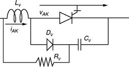
FIGURE 26.11 Typical GTO combined diAK/dt and dvAK/dt snubbers.
The above-mentioned drawbacks bound the application of GTO-like semiconductor devices to high voltage and high current applications, where the low on-state voltage is mandatory for high efficiency, but the switching speed, gate-drive power and reliability are not at concern.
The GTO device is difficult to protect against short-circuit currents due to its long storage time, long turn-off delay, and comparatively low turn-off current capability.
Some GTO-derived devices, such as the Integrated Gate Commutated Thyristor (IGCT) and sometimes the GCT, incorporate distributed gate drives in close association with the GTO, being a single device thus improving reliability [18]. This approach tries to circumvent the gate wiring inductances and enables accurate control of the turn-on speed. It is useful for series association of IGCTs, including overvoltage and short-circuit protections, together with redundancy. Still, the gate power is significant, and the IGCT needs a turn-on snubber.
Some GTO devices integrating MOSFET-based distributed gate turn-off drivers, with very low gate stray inductances, are sometimes called MOS Turn-off Thyristors (MTO) [13] (Fig. 26.12a). They have the potential to block up to 9 kV and can be faster than the GTO itself, although they need hybrid gate drives to turn-on.
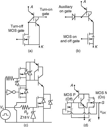
FIGURE 26.12 Functional equivalent models of (a) MTO; (b) ETO; (c) conceptual ETO driver; and (d) MCT.
If low-voltage, high current MOSFETs are connected in series with the GTO cathodes (cascode connection) and are used to turn-on and turn-off the GTO, then the whole device is usually called the Emitter Turn-off Thyristor (ETO) (Fig. 26.12b) [13] and has higher switching speed, higher reliability, and easier gate drive than the GTO itself. The ETO on-state voltage can be lower than in a comparable IGBT and even lower than in IGCT/GTOs. Thus, emitter-switched GTOs can present efficiencies and switching speeds higher than comparable high-voltage IGBTs or IGCTs at 4.5 kV, 4 kA, although at higher costs than IGBTs, but lower than IGCTs or even GTOs. Like IGCTs, ETOs include a GTO and need a turn-on snubber, but can be fully optical fiber controlled (stray and electromagnetic interference reduction). The ETO drivers can easily generate the needed gate power (self-gate-drive power), including minimum on/off time generation needed by the GTO, voltage, current, and temperature sensors, and easy over-current protection (MOS turn-off).
The MOS Controlled Thyristors (MCT) [13] are silicon fully integrated devices that try to improve GTOs, using integrated both turn-on and turn-off MOS devices (Fig. 26.12d). They can have lower on-state losses than IGBTs, current densities high than IGBTs, working temperatures up to 200°C, and block forward voltages of few kV. Switching speed is high than in the GTO or even in the high voltage IGBTs. The MCT promises to withstand much higher values of dvAK/dt and diAK/dt than GTOs, needing almost no snubbers and benefiting of simple MOSFET-like gate drivers. As MOSFETs, MCTs can easily be connected in series or parallel associations to increase their voltage or current ratings.
26.2.4 Power JFETs and Derived Devices
Power Junction Field Effect Transistors (JFET) (Fig. 26.13), also termed Static Induction Transistors (SIT), are short-channel, depletion-type junction field-effect devices operating in the prepunch through zone [13]. Their operation depends on the flow of majority carriers (electrons) only (unipolar device), and they have very low stray capacitances. Therefore, SITs have low switching losses and the potential to switch at very high frequencies, even higher than MOSFETs, up to the THz band.
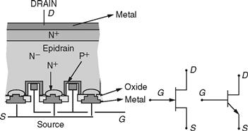
FIGURE 26.13 Power JFET structure and possible symbols.
The SIT is normally-on device (with vGS = 0, it is in the on-state) that turns off by applying negative gate-source voltages vGS < 0, up to several tens of volts. The vGS negative voltage reverse biases de PN gate-source junction, pinching-off the conducting epi-drain and interrupting the flow of majority carriers.
Unlike SCRs, GTOs, MOSFETs, or IGBTs, the SIT normally-on property enables its use in high-speed pulse generation circuits similar to those of SOS diodes, the main difference being the controlled turn-off with a negative gate voltage vGS ≈−vDS/ν, where ν is the SIT blocking gain ν ≈ ΔvDS.
The normally-on property of the SIT can increase its gate-drive circuit complexity. A power IFET usually requires larger power and gate voltages compared with a similar MOSFET These two SIT drawbacks can be advantageously solved using a cascode connection (Fig. 26.14a) in which a IFET is source switched by a low-voltage, high current MOSFET.
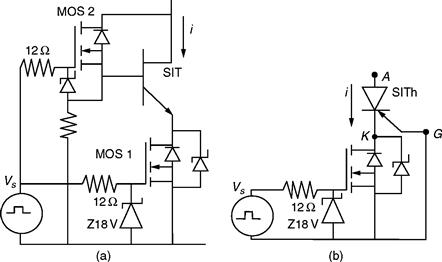
FIGURE 26.14 (a) JFET cascode using two MOSFETs. MOS2 can be used to operate the SIT in the bipolar mode; (b) SITh cascode.
The SIT device presents positive temperature coefficient, enabling easy paralleling like the MOSFET, and is a unipolar voltage-controlled device enabling relatively easy series connection. The SIT does not need turn-on or turn-off snubbers; simple RC clamping circuits (Fig. 26.15) are enough for stray inductance overvoltage protection.
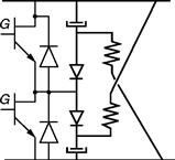
FIGURE 26.15 SIT voltage clamper.
The SIT can be operated in the bipolar mode (called Bipolar Mode SIT, BSIT, or BMSIT), if they are designed to allow positive gate currents to inject holes in the drain channel. The on-state of the BSIT is almost like that of a bipolar carrier device, increasing the turn-off time, but current density is much higher and useful phenomena for pulsed power might occur [10, 11, 13].
A SIT-derived structure which is being used in pulsed power is the static induction thyristor (SITh) also called Field Controlled Thyristor (FCTh) or Field Controlled Diode (FCD). It includes (Fig. 26.16) a P+ layer (instead of the SIT drain N+ layer) to obtain a PN junction (hence the name pinched diode). Present SITh devices block 4 kV and can switch peak currents in the kA range, presenting long lifetimes.
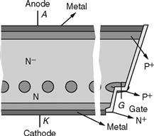
FIGURE 26.16 Typical SITh (GTO-SIT) structure.
The SITh behaves like a diode if vgk = 0 (gate-cathode short). This diode can be turned off with almost no reverse recovery, making vGk negative. However, the depletion capacitance gate current to turn-off can be as high as half of the anode current, making the SITh gate driver difficult to design and operate. An alternative to ease the gate driver is to use a cascode connection (Fig. 26.14b).
The SITh is being used for pulse generation as an opening switch in inductive circuits (Fig. 26.17), much like the SOS diode (the SITh behaves as a controlled diode), and holds the pulse voltage Vp during the output phase. The gate current needed to extract carriers out of the device, to cause depletion and the off-state, is obtained by switching off the inductive current (with the cascode SITh) in a step-up auto-transformer. The switching-off induces the negative, fast rising vGK voltages necessary to extract SITh carriers and to apply the load pulse. Speed switching in this case can be enhanced by positive feedback, the fast gate current decay creating a depleted SITh that helps in turning off the current.
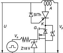
FIGURE 26.17 SITh cascode pulse generation using magnetic energy storage.
Much attention is being devoted to new SITs based on silicon carbide (SiC) structures and their derived devices, which can switch voltages in the kV range and current near the kA, specially the 4H-SiC SIT cascodes, which are expected to attain 8-10 kV blocking voltages. Other semiconductor materials such as gallium arsenide (GaAs), gallium nitride (GaN), and Superjunction Structures (SJ) are being investigated to build SJ power MOSFET structures, Super Trench MOSFETs (STM), Vertical Deep Trench (Resurf DMOS –VTR-DMOS), SJ DMOS and UMOS, SITs, and SIT-derived structures [4]. The GaAs SIThs are expected to be faster devices than existing power semiconductors.
26.2.5 Semiconductor Series Stacks and Generalized Cascodes, Semiconductor Parallel Stacks
26.2.5.1 Semiconductor Series Stacks
For applications where the needed working voltage is higher than the available semiconductor ratings, one possible solution is to series connect several power devices. Steady state and transient balance or sharing of the voltage between series semiconductor devices are very important, since most power semiconductor devices do not hold voltages above their rating and their reverse currents and reverse recovered charges differ from device-to-device even within the same type and maker, the semiconductor with the least reverse leakage current will hold higher voltages.
EXAMPLE 26.3 Consider a string of two series diodes and suppose the total voltage U = 10 kV, the two diodes both with nominal repetitive reverse voltage VRRM = 6 kV, but reverse leakage currents of IRmax = 40 mA, and IRmin = 10 mA. Calculate the diodes reverse voltages.
SOLUTION. We can calculate Reqoffmin =VRRM/IRmax = 150 kΩand Reqoffmax =VRRM/IRmin = 600 kΩ(Fig.26.18). Therefore, the diode with Reqoffmin would have the voltage VReqoffmin = 10 × 103 × 150/(150 + 600) = 2 kV, while VReqoffmax=lQ × 103 × 600/(150 + 600) = 8 kV that exceeds the diode maximum rating. This diode would operate near its avalanche voltage (≈ 6 kV), which could be destructive.
Steady-state balancing can be achieved using high-value parallel resistors Rh, so that the parallel of Rh, with Reqoffmin, or Reqoffmax should give a resistance able to maintain the semiconductor reverse voltage within acceptable limits.
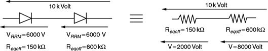
FIGURE 26.18 Series connection of power semiconductors.
Considering n-series-connected power semiconductors and one of them with IRmin = 0 (Reqoffmax≈∞), while the remaining n –1 have the typical value Reqoff, the total value RT of the string of resistors is RT=Rh + (n − l)(Rh||Reqoff) (Fig. 26.19). The maximum voltage occurs in the diode with Reqoffmax≈∞ being VRmax = URh/RT. This value should observe a safety margin U/n < VRmax < κVRRM, where κ < 1, that permits to obtain n > U/VRmax and <Rh =Reqoff(nκVRRM–U)/(U.κVRRM). Note that U > κ VRRM and nκVRRM > U.
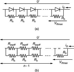
FIGURE 26.19 (a) Steady-state balancing a series connection of power semiconductors; (b) Equivalent model.
The Rh resistors should be as high as possible to minimize their dissipated power. The maximum Rh value can be obtained considering the IRmin and IRmax semiconductor currents (instead of IRmin = 0) to obtain Rh < (nκVRRM –U)/[(n − 1)(IRmax –IRmin)].
An alternative to the use of the dissipative resistors is to antiparallel avalanche or Zener diodes or Metal Oxide Varistors (MOV) with each series device.
To help share the voltage during transients, RSCS parallel snubbers must be also included (Fig. 26.20). If they are designed just to balance the reverse recovered charge QRR, then the capacitor value can be given by CSmin≈ Δ QRR/ Δ U, Δ U is the allowed voltage mismatch and Δ QRR is the QRR variation among devices. Resistor RS limits the discharge current when the power semiconductor turns on.
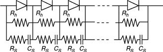
FIGURE 26.20 Dynamic- and steady-state balancing of seriesconnected power semiconductors.
To operate the RSCS as a parallel snubber, the circuit associated stray inductance LS should be estimated. Assuming energy conservation, a rough estimation of theCS value is CS ≈ LSI2RR/[n(κVRRM)2]. Resistor RS should define the damping factor τ of the equivalent RLC circuit, being ![]() . For controlled turn-on and turn-off devices, the RsCs parallel snubber can be improved using an extra diode (RVCVDV in Fig. 26.11, with LV = LS). To obtain near-balanced turn-on tr and turn-off tf times for each series semiconductor, with direct current IAK, hold-off voltage κVDRM and pulse on minimum time Tpmin, LS should have the value LS ≈ κVDRMtr/IAK and CV ≈ IAKtf/(κVDRM), beingRV ≈ Tpminτ2/(πCV).
. For controlled turn-on and turn-off devices, the RsCs parallel snubber can be improved using an extra diode (RVCVDV in Fig. 26.11, with LV = LS). To obtain near-balanced turn-on tr and turn-off tf times for each series semiconductor, with direct current IAK, hold-off voltage κVDRM and pulse on minimum time Tpmin, LS should have the value LS ≈ κVDRMtr/IAK and CV ≈ IAKtf/(κVDRM), beingRV ≈ Tpminτ2/(πCV).
26.2.5.2 Generalized Cascodes
To use a series stack of controlled turn-off semiconductors such as MOSFETs, SITs, or even IGBTs, the generalized cascode association (Fig. 26.21) is a valuable alternative to the simple series connection [10, 14, 15]. The simple series association of turn-off devices usually needs optical fibre isolated gate drivers fed from transformer isolated current source power inverters with series connection through high-voltage closed-loop cables, to assure the insulation between the voltage levels.
FIGURE 26.21 Generalized cascade associations: (a) using SIT devices; (b) using only MOSFETs; and (c) alternative connection of gate capacitor.
The Cascode association is faster than other associations when unipolar carrier semiconductors such as MOSFETs or SITs are used. For MOSFET devices (Fig. 26.21b), the capacitor C must hold the charge to turn the MOSFET on, being Ca ≈ VGSCG/(VDSoff –VGS). Zener diodes should be used to protect the gate-source oxide. In Fig. 26.21b, the charge-holding gate capacitors are placed in a configuration where the m capacitor Cm should have the value Cm ≈ Ca(n − m + 1), n being the total number of MOSFETs and m > 1 [15].
For stacking IGBTs, care must be taken when designing the drivers of the totem pole IGBTs [20, 21]. The positive voltage of each driver can be obtained from the capacitor of the below RSCS snubber through a blocking diode connecting the resistor Rs to a turn-off MOSFET driving the IGBT [20, 21]. The Cs capacitor should hold the needed charge to turn-on the IGBT.
When dealing with cascodes, it is mandatory to minimize the source (or emitter) inductances as they can badly affect the charging rate of the gate capacitances. Bare chips (bare dice) and surface mount design should be used, instead of packaged MOSFETs, IGBTs, or SITs.
26.2.5.3 Parallel Stacks
Parallel associations of power devices can be used when the available semiconductors do not present the needed current ratings.
For positive temperature coefficient devices such as MOSFETs, SITs, and most of their derived structures, the devices can be just connected in parallel, taking care of symmetry to minimize stray inductances and capacitances and to balance junction temperatures. Individual gate drivers and protection circuits (except if stray effects are not a concern) should also be used. This is not valid for the MOSFET intrinsic diode, which must be disabled.
For negative temperature coefficient devices such as diodes, thyristors, bipolar transistors, GTO, and other bipolar devices, several methods could be used as follows:
a. To select devices with very small relative parameter variations (matched devices) and to balance their junction temperatures by using a single heat sink and symmetrical disposition;
b. To use current sharing transformers or coupled inductors (Fig. 26.22);
c. To use current feedback control techniques [22] if the paralleled devices have turn-off capability;
d. To use small resistors in series with each power semiconductor device (Fig. 26.23), calculated upon the maximum, minimum, and typical device parameters. It is possible to show that a rough estimate for the series resistor RE is RE ≈ (V1max–V1min)/(I2 −I1) [10], where V1max is the device family maximum on voltage at the minimum allowed current I1, and V2min is the device type minimum on voltage at the maximum allowed current I2 (I2 > I1).
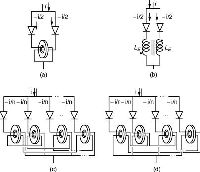
FIGURE 26.22 Using transformers or coupled inductors for paralleling power devices: (a) two diodes; (b) modeling the parallel connection of two diodes; (c) and (d) two ways of connecting n-paralleled power semiconductors.
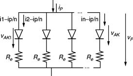
FIGURE 26.23 Parallel connections of power semiconductors using current sharing resistors.
One of the previous approaches has to be selected upon the pulsed power application to minimize costs and maximize performance.
26.3. Load Types and Requirements
Pulsed power applications present some of the most demanding loads to the modulators in terms of pulse requirements, as, normally, almost rectangular pulses are needed to many applications in capacitive and inductive loads.
Nowadays when evaluating a PP modulator topology, it is important to consider, in addition to cost, size, simplicity of operation, and efficiency, the flexibility for different operating conditions into various load conditions (i.e., resistive, capacitive, and inductive).
In fact, the growing variety of environmental, biological, medical, and industrial applications using positive or negative high-voltage repetitive pulses, for enhancing the characteristics of a product or method, impose various load conditions to the modulator circuits [23].
For example, applications with plasmas or gases present normally capacitive behavior, like plasma implantation or air processing for pollution control [24, 25]. Applications that use coils present an inductive behavior, like electromagnetic forming, or whenever a high-voltage transformer is associated to the modulator to further increase the output voltage [26, 27]. In addition, food processing and water treatment present resistive behavior.
26.3.1 Resistive (R) Loads
Pure resistive-type loads are not common in pulsed power applications, being the processing of liquids one of the exceptions, in applications such as liquid food sterilization, waste water decontamination, and biomedical materials. However, resistive loads are used frequently as a load reference for testing and comparison of the pulse voltage waveform between different types of modulators.
The problem is to find a resistor that can handle the generated power, the voltage level, at the same time, without presenting inductive behavior. There are expensive commercially available types for HV and kW operations, alternatively, it is possible to fabricate, much cheaper, water resistors for any power and voltage needed.
A water resistor is essentially an insulator tube filed with an aqueous electrolytic solution and a metal electrode in each extremity, capable of dissipating the average power and holding the high voltage from the modulator. Typically, it is made up of dilute solution of copper sulfate (CuSO4) in deionized water (a good electric insulator), which does not degrade the copper electrodes, the higher the CuSO4 concentration the lower the resistance, being the total resistance proportional to the length of the tube [28].
The energy dissipated in the water produces a change in its temperature Δt, which can be determined by knowing the specific heat of water, Cp,
(26.1) ![]()
where Q is the change in thermal energy, and m is the mass of the water resistance tube.
Nevertheless, the use of water resistances brings some limitations. First, with the temperature increase, air bubbles are formed that change the resistance value. Second, the CuSO4 molecule breakdown linked with electrolyses phenomenon has undesirable results: (1) gas release that increase the pressure inside the tube, a gas release aperture is advisable in the tube edges to prevent the increase of the pressure inside the tube; (2) the metallic copper decomposition in the cathode (i.e., copper transport from the anode to the cathode), changes the test conditions. With time, the performance of a water resistance may change in consequence of these effects.
EXAMPLE 26.4 Consider a HV pulse modulator that produces a 20kV/10 A pulse during 10 μs with 100 Hz repetition rate. Calculate the temperature increment of l= 1 –m tube (made from insulating material) with an internal diameter of d = 2.5 cm when used as a load to the modulator during 60 s.
Solution. The energy per pulse is
![]()
The energy in 60 s is
![]()
The volume of water inside of the tube is
![]()
Then, considering that 1 calorie = 4.2 J, results in
![]()
Hence, for an initial water temperature at 25°C, after 60 s, the temperature will reach up to 30.8∞C.
26.3.2 Capacitive (C) and RC Loads
Pulse power applications associated with plasma and gas processing, and occasionally liquids, present typically capacitive behavior to the PP modulators. In fact, some of the most challenging operating conditions are related with the operation with plasmas.
A typical example is plasma-based ion implantation (PBII) where a target is immersed in a plasma, produced in a confined volume, and almost rectangular negative HV pulses are applied to it. This results into a high current peak at the beginning of the pulse, rapidly decreasing to a much smaller value. The initial transient current that charges the main system capacitances can be several orders of magnitude greater than the stationary current at the pulse end, when the load imposes almost open-circuit impedance, presenting an additional challenge to the modulator. The above load dynamic characteristics can be represented in an RC electrical equivalent circuit as in Fig. 26.24 [29, 30].
FIGURE 26.24 Simplified electrical equivalent circuit of a PBII load.
For plasma loads such as PBII, considering plasma characteristics and typical wanted results, the modulator requirements can be sought: (a) the voltage pulse waveform must be independent of the load impedance; (b) the pulse rise time must be in the order of the microseconds and small compared with the pulse width; (c) the pulse duty cycle must be a few percent; (d) the pulse width and frequency should allow some load variation; (e) there must be a current limit in case of short circuit; (f) in order to be practical, the power supply cannot be too complex and bulky while including all the necessary protection systems for personnel and equipments.
In capacitive-type loads, it is extremely important, also, that the modulator topology has the capability to short circuit the load after the HV pulse, quickly discharging all the load and parasitic capacitances to zero, otherwise the load stays charged to almost full pulse voltage.
26.3.3 Inductive (L) and LR Loads
Inductive-type loads are present when a pulse transformer is used to further increase the voltage level of a modulator or when voltage pulses are applied to inductive loads such as coils. An example of the last is electromagnetic metal forming application (EMF), where HV resonant topologies apply kiloampere current pulses, during hundreds of microseconds, into very low-inductance systems [8].
For inductive operation, the modulator must clamp the load with an opposite polarity voltage after each HV pulse, during enough time to guarantee a zero average load voltage. In general, this is not accomplished with turn-off capability semiconductor switches but rather with freewheeling diodes. Also, the topology can either be dissipative or it can send the energy stored in the magnetic circuit back to the power supply, increasing the efficiency of the modulator.
26.4 Solid-State Pulsed Power Topologies
The use of innovative techniques, supported on dc–dc isolated converter topologies, brought from solid-state power electronics, taking advantage of all the capabilities of such devices, circumventing their limitations, is playing an important role to the expansion of pulse power technology to a wide range of new applications, needing compact, small size, and efficient pulse modulators, spreading to almost every industrial and commercial fields, from food sterilization, biomedical applications, and pollution control to surface engineering [30–35].
Nevertheless, each pulsed power application represents a different challenge for the pulsed power technology and the load requirements normally imposes limits to the use of each type of power converter topology. One important characteristic associated with many pulse power applications is the low duty ratio, D, pulse operation (i.e., usually lower than 5%, [1, 2]), where the pulse width is much shorter than the pulse period, which reduces significantly the modulator average power and also the dissipated power into the load, as
(26.2) ![]()
where Vp and Ip are, respectively, the pulse voltage and current amplitude, supposing a rectangular pulse with D = ton/T duty ratio.
In order to take the most of each topology and also to be able to extend these concepts to other topologies that have potential for high-voltage pulsed generation, it is important to understand the concepts and to know the advantages and limitations when using each topology.
In this section, several topologies capable of generating high-voltage pulses based on relatively low voltage semiconductors devices are analyzed. The study begins with the most common configurations for pulse generation that switch the HV voltage directly into the load, using stacks of series semiconductors.
The DC–DC isolated converter topologies, forward, flyback, full-bridge, and half-bridge, which can be modified to produce high-voltage rectangular repetitive pulses, with techniques that enable the use of relatively low semiconductor devices, are presented in the next section. Here, the use of a step-up transformer provides galvanic isolation and further increases the output voltage pulse amplitude, although the transformer presents limitations to its use. In order to overcome various technical hitches in assembling a unique high-voltage circuit, stacked associations of lower voltage topologies are also discussed with and without the use of output transformers. Finally, the mature Marx generator pulse power topology is discussed with the intensive use of semiconductors. This concept is also proposed for distributing the voltage in series stacks of semiconductors.
It is important to define some of the pulse parameters mentioned in the following sections, as shown in Fig. 26.25 for the practical shape of unipolar voltage pulses.
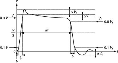
FIGURE 26.25 Practical shape voltage pulse waveform.
Considering Fig. 26.25, the voltage pulse can be characterized by several parameters:
• rise time, tr: period of time from 0.1 to 0.9 V, where V is the plateau amplitude of the pulse;
• overshoot, Δ VS: voltage excursion, after the rise time, above the pulse plateau V;
• width, Δt: pulse duration in the 0.5 V region;
• undershoot, Δ Vd: voltage excursion, after the fall time, below minimum voltage, 0 volt;
• droop, Δ V: in relation to the plateau amplitude V, Δ V= V –Vf;
• fall time, tf. period of time from 0.9 to 0.1 Vf, where Vf is the final pulse voltage, different from V because of Δ V;
• tail: voltage descend during pulse fall.
26.4.1 Direct Switching
The most straightforward technique for high-voltage pulse generation consists in switching directly the voltage from a dc capacitor bank charged with high voltage into the load, using a floating or a grounded switch, as shown in Fig. 26.26 and Fig. 26.28, respectively.
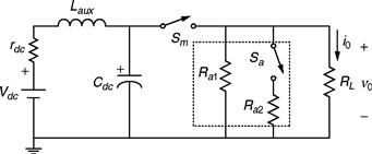
FIGURE 26.26 Direct modulator simplified circuit with floating switch.
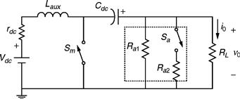
FIGURE 26.28 Direct modulator simplified circuit with grounded switch.
26.4.1.1 Floating Switch
Consider the circuit in Fig. 26.26, where the HV power supply, PS, Vdc charges an energy storage capacitor bank Cdc. The PS internal resistance added by the switch and wiring ohmic resistances is represented by rdc that limits the maximum charging current. Sometimes, a series inductor Laux is also added, which acts as a current limiter and causes some boost of the capacitor voltage during the charging period.
The voltage is modulated into the load by the series floating switch Sp, which operates with duty ratio D. The switch-onand switch-off control applies the full bank voltage to the load with the pulse width and frequency being controlled by the gate trigger. Supposing Cdc charged with Vdc, when Sm is on, during ton, the Cdc capacitor applies a voltage Vdc into the load. During this period, the inductance Laux limits the discharge of the PS to the load.
If the load has capacitive behavior, an auxiliary circuit must be added to discharge the load capacitance to zero after the voltage pulse. For low duty ratio operation or low-power operation, a permanent parallel resistor Ra1 can be connected to the load, which must hold-off the applied voltage. The Ra1 value depends on its average power dissipation
(26.3) ![]()
and the required load voltage fall time.
As an alternative, for high duty ratio operation or high-power operation, it is preferable to use an auxiliary series switch Sa with Ra2 to short the load after the pulse. In this case, the value of Ra2 can be significantly reduced.
The main advantages of Fig. 26.26 topology are associated with the generation of voltage pulses with low rise time, low voltage droop, and also the flexibility to change the frequency and duty ratio operation. However, the pulse characteristics are limited by the energy stored in the capacitor bank and on the performance and power dissipated in the switches, and also on the rate of charge of Cdc.
The energy initially stored in the Cdc capacitor is
(26.4) ![]()
if the S off time, T –ton, is enough for the PS Vdc to charge Cdc. Following, during ton, the energy delivered to the load is
(26.5) ![]()
For PP applications, only a small fraction of the stored energy should be transferred to the output during the pulse mode, otherwise the pulse voltage has a typical RC discharge waveform, as shown in Fig. 26.27, and not an almost rectangular shape, as shown in Fig. 26.25.
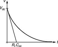
FIGURE 26.27 Typical RC discharge waveform.
For a resistive load, the pulse voltage decay Vdcf can be calculated as
(26.6) ![]()
Considering a resistive load RL, the capacitance of the Cdc capacitor (Fig. 26.26 circuit) can be determined according to energy delivered to the load. For the required pulse voltage droop Δ v0,
(26.7) ![]()
where VCdcf is the capacitor voltage at the end of pulse, ton, and VCdci is the capacitors voltage immediately before the pulse. Considering (26.7), the difference between (26.4) and (26.5) is the energy stored in the Cdc capacitor at end of pulse mode, ECdcf,
(26.8) ![]()
where (26.8) for this case results in
(26.9) ![]()
considering that VCdci = Vdc. Equating (26.9), the capacitor value should satisfy the condition
(26.10) ![]()
Considering (26.3) through (26.10), it is mandatory to store in Cdc an energy greater than five times the pulse energy in order to have an output voltage droop better than 10%, but if a 1% voltage droop is expected, a 50 times storage energy is required, which may impose limits to the design of the modulator.
In addition, the Vdc power supply must be able to recharge the Cdc capacitor with an energy equal to the delivered pulse energy, E0, plus losses, during the charging, T –ton, and pulse, ton, periods
(26.11) ![]()
During the initial charging of the capacitor Cdc, the PS takes a longer time in order to limit the power dissipation in the Rdc resistor.
The main disadvantages associated with the circuit in Fig. 26.6 are the Sm switch floating trigger terminals, resulting in a trigger signal that must be transmitted with galvanic isolation. Also, switch Sm must hold the total Vdc voltage during the off period, T –ton, and conduct the load current during the on period.
EXAMPLE 26.5 Consider the HV pulse modulator of Fig. 26.26, where Vdc = 20 kV. Calculate the value of the capacitor Cdc for applying 50 μs, 1600 Hz, into a RL = 1 kΩ load, and the minimum power of the power supply, Vdc, considering 20% losses during the charging and pulse modes.
SOLUTION. Considering the capacitor Cdc initially charged with Vdc and a voltage droop of 5%, then (26.7)
![]()
which results (26.3)
![]()
Choosing a 1.2 μF, then the energy stored in Cdc initially is
![]()
The energy delivered to the pulse is
![]()
This means that after the pulse, the energy stored in the Cdc capacitor is 220 J, corresponding to a final pulse voltage of 19.149 V that is 4.2% voltage droop.
Finally, the PS Vdc must recharge the 20 J, plus 4 J (i.e., 20% losses) in T –ton = 625 μs, then
![]()
26.4.1.2 Ground Switch
It is possible to connect the switch Sm referenced to ground and the Cdc capacitor floating as shown in Fig. 26.28. Considering Fig. 26.27 circuit, when Sp is off, the Cdc capacitor is charged through the load. Supposing Cdc charged with Vdc, when Sm turns on the positive terminal of Cdc is grounded and a voltage of Vdc is applied into the load.
The main advantage of Fig. 26.28 configuration in relation to Fig. 26.26 is that Sm is grounded, which makes the triggering process easier. However, in the Fig. 26.28 circuit, during the pulse period ton, the Vdc power supply is shorted, increasing dramatically the power dissipation in Rdc, which is a significant disadvantage that limits the operation to very low duty ratios.
If inductive-type loads are to be connected in both circuits, it is mandatory to use a free wheeling diode in parallel with the load to reset it after the pulse and, also, to maintain the magnetic energy continuity.
26.4.1.3 Series Stacks of Semiconductors
Considering the dozens of kilovolt range pulse amplitude in the majority of pulsed power applications and the limited maximum reverse voltage of semiconductor switches, such as power BJT, MOSFET, IGBT, GTO, and IGCT, it is necessary to connect many semiconductors in series to assemble the Sm and Sa switches in Fig. 26.26 and Fig. 26.28, as shown in Fig. 26.29 [36–41].
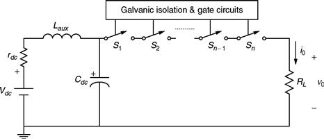
FIGURE 26.29 Series-stacked semiconductor topology for high-voltage pulse generation.
As seen, sharing resistors for steady state and RCD snubber circuits for transient voltage balance are needed for on-off-controlled semiconductors. In addition, it is complex to synchronously trigger many devices in series, placed at different floating high-voltage potentials.
Gate-control delay techniques, or generalized cascades, are used to force the synchronized operation of semiconductors with mismatched switching on/off characteristics [42].
Nevertheless, in order to prevent shutdown of a series-stacked semiconductor switch due to a defect arising in one semiconductor, redundant switches are, usually, included in the series, about 20% more, such that the surviving semiconductors share the voltage and the failed semiconductor is still able to carry the load current. This is true since the power switches used are built to short circuit when failing [43].
In order to decrease the voltage hold-off stress on the semiconductors, it is possible to add a high-voltage step-up pulse transformer in the output, further increasing the output voltage to the desired amplitude. However, several following issues must be taken into consideration before designing the circuit [44–47]:
1. The parasitic elements (i.e., distributed capacitance and leakage inductance) normally associated with the assembling of the transformer impose limitations to the output pulse waveform, degrading the pulse rise time and voltage plateau;
2. The transformer core volt-seconds product limits the transformer flexibility to accommodate different operating conditions, such as, duty ratio and frequency;
3. After the pulse, it is mandatory to reset the transformer core magnetic flux back to the initial status before the next pulse, which imposes an auxiliary circuit.
Some of the topologies used in power electronics, designed for dc–dc isolated converters, can be specially modified for pulse generation, where the addition of the transformer gives the galvanic insulation and contributes to the reduction of the hold-off voltage in the semiconductors as described in the following sections.
26.4.2 DC–DC Isolated Converters
The use of classic high-voltage modulator topologies, such as the ones described in the previous section, substituting the hard-tube switches by stacked semiconductors is frequently not the best solution for high-voltage pulse generation when using semiconductors, due to the still high-voltage limitations of the devices and their sensibility to over-voltage and over-currents.
Alternatively, it is advantageous to take into account the topologies that were originally designed for power semiconductors such as the dc–dc isolated converters. The literature refers the use of full-bridge, half-bridge, forward and flyback converters in hard-switching and resonant topologies for applications such as rapid capacitor high-voltage charging, food processing, X-ray, plasma processing, and air and water pollution control [32–35].
The use of a transformer for galvanic isolation in the forward converter, derived from the buck dc–dc converter, the flyback converter, derived from the buck-boost DC–DC converter, and the bridge topologies can significantly reduce the voltage stress on the semiconductors. In this section, the focus is placed on the particular characteristics that enable high-voltage pulse generation, using relatively low-voltage semiconductor devices.
As the objective is to generate high-voltage pulses at the output, several changes must be introduced in the typical topologies and operating conditions of these circuits. The most obvious is the elimination of the output LC filter used to keep the output voltage nearly constant.
In the following analysis, it is considered that the semiconductors switches have ideal switching behavior, instantaneous commutation times, zero voltage drop, and zero leakage current.
26.4.2.1 Forward Topology
The simplified forward-type circuit used to generate negative unipolar high-voltage pulses into a load is shown in Fig. 26.30 and the theoretical key waveforms are shown in Fig. 26.31. For positive unipolar pulses, the ground should be placed on the opposite secondary transformer terminal. The auxiliary RCD voltage clamp circuit connected to the transformer primarywinding is used to reset the transformer using the lowest constant voltage. Considering that the RCD clamp capacitance Cs is sufficiently large, the voltage Vc across it can be assumed constant [48, 49].
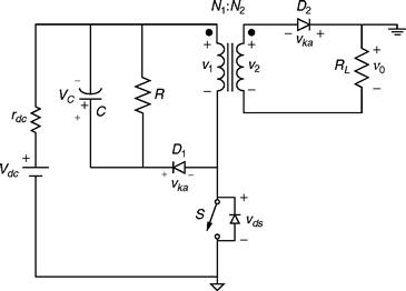
FIGURE 26.30 Simplified layout of the pulsed power forward-type circuit used to generate negative, high-voltage pulses to a load.
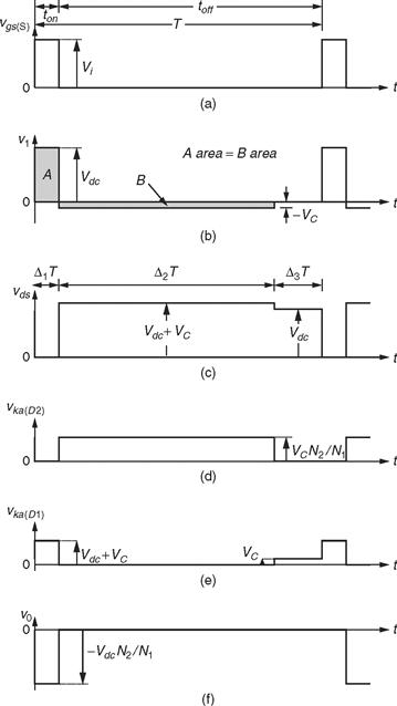
FIGURE 26.31 Theoretical key waveforms for the circuit in Fig. 26.30, for a resistive load: (a) switch-trigger signal vgs; (b) primary winding voltage, vi; (c) switch voltage vs; (d) D2 reverse voltage; (e) D1 reverse voltage; and (f) load voltage v0.
For pulse generation, the circuit operation can be explained considering only three operating modes [32, 50]. In the first mode, the pulse mode, when the main switch S is turned on during Δ1 T = DT = ton, where D and T are, respectively, the S duty ratio and operating period, the energy is transferred from the transformer primary winding circuit to the output. As the voltage applied to the transformer primary winding N1 is Vdc, the secondary winding N2 diode D2 is on, thus the voltage applied to the load is
(26.12) ![]()
where N2/N1 is the transformer turns ratio, N. In addition, the RCD diode D1 is off, with a reverse voltage of
(26.13) ![]()
For a resistive load RL, the pulse amplitude is given by
(26.14) ![]()
In the second mode, the reset mode, when the main switch S turns off, the RCD diode D1 goes on and the voltage applied to transformer primary winding is –VC, which resets the transformer core. During this time, Δ2 T, the secondary diode D2 is off, holding off a reverse voltage of
(26.15) ![]()
which results into a zero-load voltage. From (26.15), the lower the VC voltage and the transformer turns ratio N, the lower is the voltage hold-off by diode D2. In addition, the switch S must hold-off a voltage
(26.16) ![]()
where VC must be as low as possible to decrease this voltage.
Finally, in the third mode, the safety mode, following the transformer reset period, during Δ3 T, still with S off, the voltage applied to S is
(26.17) ![]()
and the voltage applied to the transformer is zero. It is important to have Δ3 T > 0 in order to guarantee a safety operating margin for the transformer core reset. For practical operation, values between 20% and 30% should be sufficient. This is done by increasing the VC clamp voltage above the calculated value.
The operation of Fig. 26.30 circuit for high-voltage pulse generation imposes several conditions as follows:
1. The use of a step-up transformer in order to decrease the voltage on the devices connected on the primary side;
2. A minimum reset voltage VC to guarantee the complete transformer core reset during the S off period, Δ3 T > 0, reducing at the same time the hold-off voltage of D2 (26.15) and of S (26.16).
Considering the second condition, it is important to understand the relation between the reset voltage VC with the operating conditions, such as the duty ratio D.
The reset voltage VC can be calculated by equating the integral of the primary winding voltage, v1, over one time period to zero
(26.18) 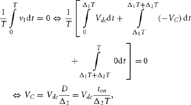
where Δ2 T = τ is the transformer core reset period.
For the boundary condition Δ3 T= 0 (i.e., Δ1 T + Δ2 T = T and Δ2 = D), (26.18) becomes
(26.19) ![]()
Substituting (26.19) in (26.15) results for vka in diode D2 results in
(26.20) ![]()
Considering (26.18) and (26.20) and introducing the load voltage module |V0| and the ratio of τ/toff, the reset time and the time switch S is off, results in
(26.21) 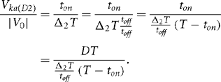
Simplifying (26.21) becomes
(26.22) 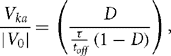
which can be represented graphically by Fig. 26.32, where
(26.23) ![]()
with Δ1 + Δ2 + Δ3 = 1 and Δ1 = D.
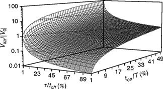
FIGURE 26.32 Graphic representation of the reverse voltage of diode D2 as a function of the reset time and duty ratio of the forward topology (26.30).
The graphie in Fig. 26.32 shows the maximum load voltage hold-off by diode D2 as a function of S duty ratio, D, and the transformer reset factor, τ/toff.
Various conditions can be presented for high-voltage pulse generation by forward converters using low-voltage solid-state devices as follows:
1. If the switching duty ratio is only a few percent, and the resetting time extends to almost all the main switch-off time (i.e., Δ2 T + Δ3 T), diode D2 holds off a small fraction of the output voltage;
2. If a step-up transformer is used, N ![]() 1, this topology enables, also, the use of low hold-off voltage semiconductors in the primary transformer side, when compared with the output load voltage.
1, this topology enables, also, the use of low hold-off voltage semiconductors in the primary transformer side, when compared with the output load voltage.
For safety reasons in order to ensure that the transformer core is fully reset, the transformer resetting time must end before the off state of the S switch ends, Δ3 T > 0.
The short duty cycles required for generation of HV pulses with low-voltage semiconductors is not a shortcoming, as most PP applications require short-pulse widths and large recovery times.
Much care should be put in the design and assembling of the transformer as this element must sustain the HV between its terminals. In addition, this topology requires the polarity of the primary winding of the transformer to be identical to that of the secondary winding and so the energy of the load is obtained during the on-state of the switching device. Therefore, it behaves like a true transformer, wherein energy storage is undesirable, associated with the leakage inductance. However, the forward converter transformers have the poorest utilization and efficiency ratios, because neither the core nor the windings are used during the lengthy core reset interval.
Due to the low, main switch S duty-cycle operation and transformer behavior, the RCD clamp voltage is designed for a low current, typically, a few percent of the main circuit current.
The RCD clamp can be considered a buck-boost converter in discontinuous mode of operation, and designed so that, under any load conditions, during the S switch-off period, the transformer core is fully reset [49].
For resetting the transformer core, other solutions can be implementing, such as a third auxiliary winding, but the fact that this transformer is for HV pulse generation, limits in terms of parasitic, assembling complexity and safety.
EXAMPLE 26.6 Suppose the generation of–5 kV amplitude pulses with 5 μs and f = 10 kHz (D = 5%) from the circuit in Fig. 26.30. The circuit is supplied from a mains transformer at Vdc = 500 V and a N=10 pulse transformer is used. Calculate the semiconductor switches S, D1, and D2 hold-off voltage.
SOLUTION. Consider first boundary condition (26.19), then
![]()
The semiconductors hold-off at 526.3 V for the S switch and diode D1, and 263 V for diode D2, respectively, 10.5% and 5.26% of the output voltage.
Consider now a reset factor of τ/toff ≈ 65%, then Δ1 = 5%, Δ2 ≈ 62.5%, and Δ3 ≈ 32.5%. From (26.18)
![]()
resulting in 540 V for the S switch and diode D1, and 400 V for diode D2, respectively, 10.8% and 8% of the output voltage.
Hence, for generating 5-kV pulse, 800 V semiconductors could be used, considering a 100% safety factor.
26.4.2.2 Flyback Topology
The simplified flyback-type circuit used to generate negative high-voltage pulses into a load is shown in Fig. 26.33; for positive pulses, the ground should be placed on the opposite terminal.
FIGURE 26.33 Simplified layout of the pulsed power flyback-type circuit used to generate negative high-voltage pulses to a load.
The circuit in Fig. 26.33 is similar to the circuit shown in Fig. 26.30, but the polarity of the diode D2 on the secondary winding is reversed. However, this simple change imposes completely different circuit behavior [48].
Considering the circuit in Fig. 26.33 and the theoretical key waveforms of Fig. 26.34, for boundary conditions, when the main switch S turns on, the energy is stored in the transformer as magnetic flux, the transformer must act as a coil storing energy. The voltage applied to the transformer primary winding is Vdc; the RCD diode D1 and the secondary winding diode D2 are off, thus the voltage applied to the load is zero. The secondary diode D2 reverse voltage is
(26.24) ![]()
and the RCD diode D1 reverse voltage is
(26.25) ![]()
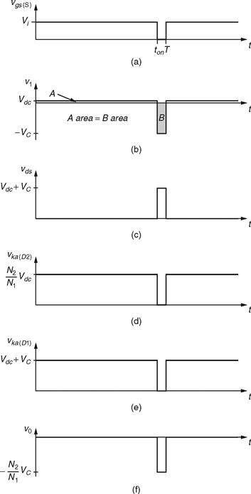
FIGURE 26.34 Theoretical key waveforms for the circuit in Fig. 26.33, for a resistive load: (a) switch-trigger signal vgs; (b) primary winding voltage, v1; (c) switch voltage vs; (d) D2 reverse voltage; (e) D1 reverse voltage; and (f) load voltage v0.
When the main switch S is turned off, the energy stored in the transformer is transferred to the output. The voltage applied to the transformer primary winding is –VC; the RCD diode D1 and the secondary winding diode D2 are on, and voltage applied to the load is, approximately,
(26.26) ![]()
The voltage hold-off the main switch S is
(26.27) ![]()
The RCD clamp voltage has two purposes: (1) reduce the voltage spike that occurs due to the resonance between the transformer leakage inductance and the switch S output capacitance, in the off state; and (2) establish the pulse voltage during the same period of time.
Considering the transformer primary winding voltage waveform given in Fig. 26.34, the clamp voltage, VC, can be approximately derived by equating the integral of the primary winding voltage, v1, over one time period to zero
(26.28) ![]()
similar to the VC voltage in the buck-boost topology (26.19).
Concerning high-voltage pulse generation [50], if the switching duty ratio is near 100%, D2 blocks only a small fraction of the output voltage. Additionally, if the RCD diode D1 is on during the S switch-off time, meaning the flyback circuit runs in continuous mode, the output voltage pulse is well defined by the RCD capacitors voltage VC. Moreover, with a step-up transformer (N ![]() 1), this topology also enables relatively low-voltage semiconductor devices in the primary side.
1), this topology also enables relatively low-voltage semiconductor devices in the primary side.
For efficiency reasons, the flyback circuit parameters should be calculated in order that the circuit works at the boundary between the continuous and noncontinuous state. This is done by assuring that the RCD diode D1 turns off at the same instant the switch S turning on. The RCD clamp voltage is sized by the main circuit current due to the high duty ratio operation of switch S and the coil-like transformer behavior.
The flyback transformer design is more complex than the forward transformer, as the energy is supplied to the load during the off state of the S switch, meaning that the transformer must be designed to store energy during the on state of the S switch, behaving as a coupled inductor.
The S switch current interruption requirements and the coupled inductor design can be much more challenging in the flyback topology at power levels of interest and represent a limitation of this topology. This is normally the realm of much higher current devices such as the IGBT and GTO or the use of parallel semiconductors.
Nevertheless, the flyback circuit is much more fault tolerant to a short circuit in the load or load faults since the switch S is in the off state during the output pulse and will not see the fault current as would the forward converter topology.
Comparing the forward and flyback topologies for HV pulse generation for the same output voltage pulse amplitude, using the same turn ratio transformer, the forward circuits need a high amplitude dc PS voltage Vdc, but the RCD voltage is lower and the switch S duty ratio is low. Also, in the flyback topology, the voltage pulse width is not as well defined as in the forward because it is generated by the RCD circuit.
Both topologies have problems in dealing with capacitive loads because the dynamic variations in the load impedance mismatch the output of the transformer. The solution requires the use of a permanent dummy load, but this increases the power dissipation. Another possibility is the use of a switch dummy load, which will put a semiconductor device in the high-voltage region.
EXAMPLE 26.7 Suppose the generation of–5 kV amplitude pulses with 5 μs and f = 10kHz (D = 95%) from the circuit in Fig. 26.33. The circuit is supplied at Vdc = 25 V and a N=10 pulse transformer is used. Calculate the semiconductor switches S, D1, and D2 hold-off voltage.
SOLUTION. Consider (26.28), then
![]()
The semiconductors hold-off at 526.3 V for the S switch and diode D1, and 263V for diode D2, respectively, 10.5% and 5.26% of the output voltage.
Hence, for generating 5-kV pulse, 800 V semiconductors could be used, considering a 100% safety factor.
26.4.2.3 Bridge Topologies
The forward and flyback topologies are suitable for the generation of unipolar HV pulses. If bipolar pulses are needed, bridge configurations should be used, like the full- and half-bridge topologies with or without a step-up transformer [32–35].
Considering a half-bridge topology (Fig. 26.35a) shows the configuration for obtaining positive pulses, where the switch S1 applies the pulse to the load, and switch S2 is capable of applying a zero voltage to the load, which can be important if the load is capacitive, as shown in Fig. 26.35b, otherwise, the load will stay charged. If antiparallel diodes are connected to the switches, pulses can be applied to inductive loads, where the S2 antiparallel diode reset the load after the pulse. For negative pulses, the circuit is presented in Fig. 26.36a, similar operating behavior applies now for opposite polarity, as shown in Fig. 26.36b.
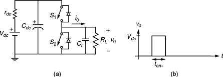
FIGURE 26.35 Half-bridge topology for generating positive HV pulses; (a) simplified circuit and (b) output voltage, v0, for a capacitive load, CL//RL.
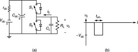
FIGURE 26.36 Half-bridge topology for generating negative HV pulses; (a) simplified circuit and (b) output voltage, v0, for a capacitive load, CL//RL.
The main limitation of this topology is the hold-off voltage of the semiconductors, which must block the same voltage as the dc HV power supply Vdc. If a transformer is connected in parallel with switch S2, its antiparallel diode can reset the transformer core after the pulse, but this is limited to low duty ratio operation due to the low-reset voltage impose by the diode.
If positive and negative pulses (i.e., bipolar) need to be generated using a half-bridge topology, then two power supplies are required, as shown in Fig. 26.37. In this case, each switch Si, must hold-off the sum of the two power supplies voltages, that is, 2Vdc. However, for capacitive-type loads, it is not possible to discharge the load capacitance after the pulse, as shown in Fig. 26.37b, since both S1 and S2 must be off.
FIGURE 26.37 Half-bridge topology for generating positive and/or negative HV pulses; (a) simplified circuit and (b) output voltage, v0, for a capacitive load, CL//RL.
In order to decrease the switches voltage hold-off, it is common to use the full-bridge topology, shown in Fig. 26.38a, which also uses one less power supply. Each switch hold-off voltage is only Vdc. The use of more switches also increases the capability to deal with different load conditions, as shown in Fig. 26.38b. In fact, with the full-bridge topology, positive and/or negative pulses can be applied to any type of load. Nevertheless, depending on the flux of energy not all the controlled turn-off switches are always required.
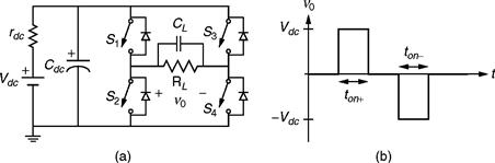
FIGURE 26.38 Full-bridge topology for generating positive and/or negative HV pulses; (a) simplified circuit and (b) output voltage, v0, for a capacitive load, CL//RL.
These topologies are used in applications such as rapid high-voltage capacitor charging, food processing, or air pollution control, where bipolar pulses enhance the process [26–30].
It is also possible to connect a transformer at the output terminals to increase the output voltage amplitude and to lower the hold-off voltage in the semiconductors switches if high-voltage pulses are to be generated, with the limitations already described. In order to limit the switches losses, it is common to use auxiliary inductors and capacitors in series or parallel configurations to couple the H-bridge to the HV transformer and also to guarantee a zero average voltage applied to the primary winding.
26.4.3 Cascade Circuits
The assembling of a single modulator circuit with very HV can be a very complex task and result in a number of problems as follows:
• Transformer assembled with very high turn ratio and voltage output;
• Many semiconductors stacked in series;
• Presence of HV in small distributed volume and safety distances;
• Coupling parasitic capacitances and inductances between devices.
In order to avoid these problems, it is possible to cascade single modulators circuits where the output voltage is the sum of the individual outputs. However, care is needed in the connection of each circuit as voltage sharing between them is essential.
26.4.3.1 Circuit without Output Transformers
In the topology shown in Fig. 26.39, there is no transformer between the energy storing capacitors and the load, the system is composed of basic pulse generator cells, made by a capacitor Ci and a switch Si, stacked in series. The challenge in this type of generator is the uniform distribution of the voltage between each cell due to the floating nature of each cells and the high dv/dt with respect to the ground occurring during the rise and falling time of the pulse. For this reason, great care must be taken in order to limit capacitance between each cell and the ground [17].
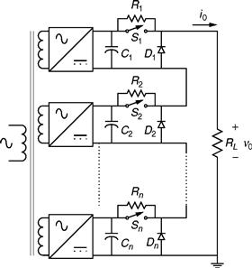
FIGURE 26.39 Series-stacked modulator topology.
For proper operation, the capacitors in each cell of Fig. 26.39 circuit need to be charged using a galvanically isolated power supply One of the possible methods includes the use of floating transformer secondary windings connected to an ac-dc converter, as shown in Fig. 26.39.
During the pulse period, the voltages of the individual cells are added up, hence the output voltage is
(26.29) ![]()
and the current through all the switches is almost the same.
The freewheeling diode Di in the output of each cell enables the switch of each cell on and off independently of other cells, which makes the system capable of adjusting the output voltage. This technique protects also the switches during the on-off commutation transient for any mismatch in the voltage distribution, where the Ri resistors help on equalizing the voltage in the Si switches during off-state (see Section 26.2.5, “Semiconductor Series, Parallel Stacks and Generalized Cascodes”).
26.4.3.2 Circuit with Output Transformers
The construction of a single, high-voltage pulse transformer, needing a high enough turns ratio (N > 1) to increase the output voltage, is complex due to the transformer’s nonideal behavior leading to significant parasitic effects as the output voltage rises. To solve this problem, it is possible to stack series several pulse transformers with lower turns ratio, in order to have only a fraction of the total voltage in each one [27, 51, 52]. With a careful design, the leakage inductance and distributed capacitances of the equivalent circuit are reduced as compared with one single equivalent transformer, leading to a better rise-time performance [53].
The most common ways to associate pulse transformers are shown in Fig. 26.40 [54]. The auto-transformer type cascade layout, is shown in Fig. 26.40a, with three transformers, each one holding one-third of the output voltage v0
(26.30) ![]()
FIGURE 26.40 Simplified transformers association: (a) cascade; and (b) secondary windings in series.
In this topology, power is supplied to Tp2 and Tp3 from the previous transformers. Transformer Tp1 and Tp2 have three secondary terminals, two of them to feed the primary of the next transformer, and the third to step up the voltage of the next transformer. This configuration decreases significantly the distributed capacitive between windings.
The major advantage of the cascade association, of Fig. 26.40a, is that the isolation voltage between windings of each transformer is the same, and equal to v0/3. However,
• Considering transformers with equal turn ratio N and primary voltage, vin, as each transformer is fed by the previous one, each transformer has a different power. Considering Fig. 26.40a, if the load power is P, neglecting the losses, in the first transformer, the input cascade power is P. The following transformer withstands 2P/3, and the third transformer withstands P/3, being the total installed transformer power 2P;
• Due to the inclusion of an extra terminal in the high-voltage side with different current ratings, the transformer assembling is complex.
Alternatively, Fig. 26.40b presents three transformers with the secondary windings in series, each one designed for one-third of the output voltage v0. In the primary side, windings are in parallel, supplied by vin, and referenced to ground. Hence, the isolation voltage between windings of each transformer is different.
Considering Fig. 26.40b, although the secondary winding potential in transformer Tp2 and Tp3, is, respectively, increased by v0/3 and 2v0/3 through the secondary winding of transformer Tp1 and Tp2, in the primary windings the reference potential stays constant. As a result, each transformer holds a different voltage between windings, depending on the series position of each transformer, which increases toward higher potentials. Thus, transformer galvanic isolation between windings must be designed to v0/3 for Tp1, 2v0/3 for Tp2, and v0 for Tp3.
The above-mentioned drawback sets serious difficulties for pulse applications of the Fig. 26.40b circuit. Since the pulse transformers placed at higher potentials hold higher voltages, the isolation distance should be increased. Consequently, the pulse waveform is distorted due to the increase of the parasitic leakage inductance with the isolation distance.
To overcome this problem, it is possible to feed the primary windings of the pulse transformers with galvanic isolated power supplies. This can be achieved with the introduction of isolation transformers, in order to keep the secondary windings of the pulse transformers in series, but with the same isolation voltage between windings. This solution has the immediate advantage that all the pulse transformers are similarly built, with the same minimum isolation distance, which helps to reduce the output pulse rise-time. Two configurations can be considered, Fig. 26.41, as follows:
• Independent isolation transformers (Fig. 26.41a);
• Cascade connected isolation transformers (Fig. 26.41b).
FIGURE 26.41 Simplified layout of series-connected secondary windings transformers fed by (a) independent isolation transformers and (b) cascade isolation transformers.
For both circuits in Fig. 26.41, the secondary windings of the pulsed transformer are series connected, delivering each one (Tp1, Tp2, and Tp3 ), v0/3 of the total output voltage v0. In the circuit of Fig. 26.41a, the primary windings of Tp1, Tp2, and Tp3 are fed, respectively, by the secondary windings of the isolation transformers Ti1, Ti2, and Ti3, these ones being fed by the input voltage vin. In this way, the pulse transformers Tp1, Tp2, and Tp3 can be assembled with the same structure and characteristics, for the same isolation voltage of v0/3. The voltage increase due to the secondary winding series connection of Tp2 and Tp3 is sustained by the isolation transformer Ti2 and Ti3. Then, for the worst running condition (considering a high capacitance between primary and secondary of the pulse transformers), the galvanic isolation of Ti2 and Ti3 must be predicted to hold, respectively, v0/3 and 2v0/3. The isolation transformer Ti1 is not necessary.
In the circuit of Fig. 26.41b, the primary windings of Tp1, Tp2, and Tp3 are fed, respectively, by the secondary windings of Ti1, Ti2, and Ti3, with primary windings fed successively by the secondary windings of the previous transformer (i.e., Ti3fed by Ti2which is fed by Ti1, which is fed by vin). In this way, the pulse transformers Tp1, TP2, and Tp3 can be assembled with the same structure and characteristics, for the same isolation voltage of v0/3. The voltage increase due to the secondary winding series connection of TP2 and TP3 is held by the isolation transformer Ti2 and Ti3 The isolation transformer Ti1 is not needed.
Taking into account the two circuits of Fig. 26.41 as follows:
• In Fig. 26.41a, considering a load power P, neglecting the losses in the transformers, each one is assembled for a power of P/3 (i.e., the power installed in all the transformers is 2P). However, in Fig. 26.41b, the pulse transformers are assembled with a power of P/3, but the isolation transformers have successive powers of P, 2P/3, and P/3. The total power installed in all the transformers is 3P;
• In Fig. 26.41b, all the transformers have the same isolation voltage, whereas in Fig. 26.41a, the isolation voltage in isolation transformers is different.
Considering only the pulse transformers, the two topologies, in Fig. 26.41, are equivalent. Hence, the choice between the two should be based on the characteristics preferred for the isolation transformers and the features desired for the pulse generator.
Regarding the last, it is considered a great advantage for the high-voltage pulse generator to be of modular construction, built upon several equal modules, where each one could occupy any position in the generator.
EXAMPLE 26.8 Consider the generation of − 15-kV pulse from a series stack of three − 5 kV forward HV pulse generators based on the topology shown in Fig. 26.30, with the operating conditions of Example 26.6. Select the stack method to implement and draw the complete assembly, taking into consideration a modular perspective. Specify, also, the energy supply to the three stages, the selection of semiconductors and their triggering.
SOLUTION. The modular high-voltage generator construction is based on three main principles as follows:
• distribute the total voltage of a high-voltage circuit by holding the potential of several points in the circuit relatively to ground;
• distribute the total voltage for several transformers connected in series;
• use isolation transformers to feed the primary of the series-connected transformers, as shown in 26.41a.
The proposed circuit layout is shown in Fig. 26.42. If positive pulses are desired, it is only necessary to invert the polarity of the secondary diodes Dri, where i ε {1,2,…, n}. Power is supplied to the three modules via isolation transformers (1:1), Tii which must hold-off a maximum voltage of 1 k kV between primary and secondary. These transformers are assembled with primary windings in parallel, connected to a dc-ac high-frequency inverter to reduce the size and increase the efficiency of the system. In addition, each secondary winding is connected to an ac–dc rectifier that produces the necessary vdci voltage to the forward converters.
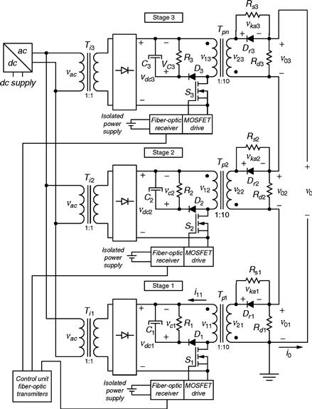
FIGURE 26.42 Modular, pulsed generator simplified layout for − 15 kV output pulses.
Considering the − 5-kV voltage at each individual forward pulse generator with the operating condition of Example 26.3, then 800 V semiconductors can be used. Hence MOSFETs can be selected for switches Si.
Considering the three modules, in Fig. 26.42, with switch Si on, diodes Dri are conducting, and the voltage applied to the load is
![]()
considering three equal modules, v01 = v02 = v03 = v0 i. During this time, the voltage reference at the secondary terminal with a dot point of each pulse transformer is raised
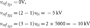
During the off time of switches Si the voltage applied to the load goes to zero, diodes Dri in each module hold-off only the reset voltage of their respective pulse transformer. Voltage-sharing resistors, Rsi, are used to equally distribute the reset voltages of each module through diodes Dri. In order to hold the high-voltage potential in each module relative to ground, high-valued Rdi resistances can also used.
Regarding the triggering of the MOSFETs in each stage, dc isolated power supplies are used in each stage to supply the necessary energy to the trigger drives that receives the signals by optic fiber from the ground control circuit.
26.4.4 Solid-State Marx Generators
The use of voltage multiplication techniques for generating HV repetitive pulses is not limited to the use of transformers. More complex methods can be used without the limitation of transformers. The most common is the Marx generator concept [55].
The Marx generator concept is presented in the circuit of Fig. 26.43, which comprises a number of modular stages constituted by an energy storage capacitor Ci, two impedances Zi (resistive and/or inductive) for charging and limiting the self-short-circuit capacitor paths and a switch Si, for i ε {1,2,…, n}. During the charging period, a relatively low-voltage dc power supply Vdc charges the Ci capacitors in parallel trough impedances Zi.
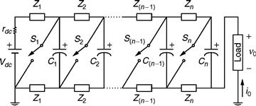
FIGURE 26.43 Marx generator topology for producing repetitive, negative high-voltage pulses into a load.
When switches Si are turned on, the Ci capacitors are connected in series and a voltage is applied into the load, equal to
(26.31) ![]()
depending on that the capacitors are charged to the power supply full voltage, Vdc. During this time, the bottom impedances Zi limit the self-short-circuit path of the Ci capacitors.
The circuit in Fig. 26.43 is assembled in such a way that there is voltage modularity, meaning that each stage holds the power supply voltage Vdc. However, due to this parallel process, the first stages carry the total charging current, which sets different power requirements for the devices in each stage.
This concept has been used intensively through the years, with spark gaps used as switch Si for very high voltages and powers, but the spark gap only turns off when the current goes to zero. Recent technological upgrades with the addition of solid-state switches and the replacement of most of the passive elements increased the lifetime of the modulator and allowed higher pulse repetition rates, meaning an improved performance [56–59].
26.4.4.1 Generation of Negative Pulses
During the last years, various semiconductors based on Marx, SM, and topologies have been described, with analogous characteristics in order to reduce the losses and increase the performance of the circuit for different types of applications and loads [56–59].
Figure 26.44 shows a typical SM topology, with n stages, able to deliver negative high-voltage repetitive pulses into a load RL, the theoretical key waveforms are shown in Fig. 26.45. Each stage of the SM consists of a energy storing capacitor Ci, a diode Dci, and two switches Sci and Spi, with antiparallel diodes, where the subscript i ε {1,2,…, n–1, n, n+ 1}. The Si switches can be implemented with BJTs, GTOs, IGCTs, IGBTs, MOS-FETS, or other on-off devices. The inclusion of Sc1 guarantees that during the pulse period, the dc charging power supply Vdc is not short-circuited, preventing high current load pulses through the power supply.
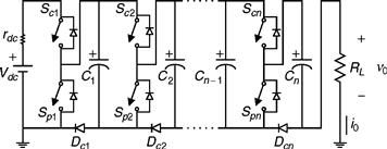
FIGURE 26.44 Circuit for applying HV-negative repetitive pulses into resistive load.
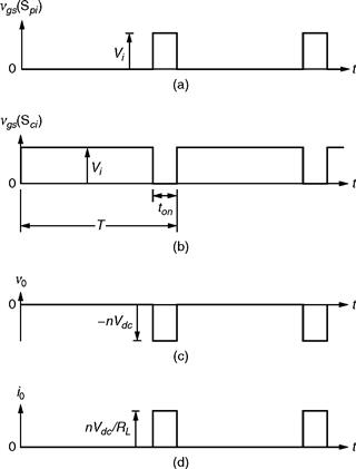
FIGURE 26.45 Theoretic waveform for the operation of the circuit in Fig. 26.44: (a) trigger signal of switches Spi, vgs(Spi); (b) trigger signal of switches Sci, vgs(Sci); (c) output voltage, v0 ; and (d) output current, i0.
Considering resistive load, RL, the operation of the Fig. 26.44 modulator can be understood considering two operating modes, for a switch duty ratio D=ton/T. In the first one, switches Sci and Spi are, respectively, turned on and turned off. During the charging period, (T-ton), capacitors Ci are charged from the dc charging power supply, Vdc, with current limited by the internal resistance of the semiconductors, wires, and the dc charging power supply internal resistance (or externally added) rdc, resulting in a small time constant that enables kHz operation. The on-state of Dci ensures that during this period, the voltage, v0, applied to the load is, approximately, zero.
In the second operating mode, switches Sci and Spi are, respectively, turn-off and turn-on. During the pulse mode, ton, capacitors Ci are connected in series and their voltage applied to the load. The load voltage v0 is proportional to the charging power supply
(26.32) ![]()
where n is the number of stages, and k < 1 characterizes the nonideal behavior of the passive and active elements in the circuit and operating conditions.
The Dci diodes guarantee, also, that the Spi switches only block a maximum voltage of Vdc, even in fault condition, such as lack of synchronization. Considering Fig. 26.44, for example, if switch Tpn is off during pulse mode, Dcn conducts and short circuits the last stage, imposing an output voltage of
(26.33) ![]()
The operation of Fig. 26.44 circuit can be represented by its equivalent model during both operating modes, considering ideal switches and Ci = C. During the charging mode, the Ci capacitors are in parallel, and the circuit can be modeled as shown in Fig. 26.46a, where nC is the equivalent capacitance, seen by the power supply, charged with Vdc. In addition, during pulse mode, the Ci capacitors are in series, where C/n is the equivalent capacitance, seen by the load, charged with nVdc, as shown in Fig. 26.46b.
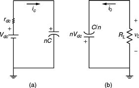
FIGURE 26.46 Equivalent circuit of Fig. 26.44: (a) the charging mode; and (b) the pulse mode, for negative output pulses.
The energy stored in the Ci capacitors, during T –ton, is
(26.34) ![]()
and the energy delivered to the load, during ton, is
(26.35) ![]()
For pulse power applications, only a small fraction of the stored energy should be transferred to the output during the pulse mode; otherwise, the pulse voltage has a typical RC discharge waveform, not an almost rectangular shape. Considering a resistive load RL, the capacitance of the Ci capacitors in the Fig. 26.44 circuit can be determined according to energy delivered to the load. For the required pulse voltage droop,
(26.36) ![]()
where VCf is the capacitors voltage at the end of pulse mode, ton, and VCi is the capacitors voltage immediately before pulse mode. Considering (26.36), the difference between (26.34) and (26.35) is the energy stored in the Ci capacitors at end of pulse mode, ECf,
(26.37) ![]()
where (26.37) for this case results in
(26.38) ![]()
Assuming that Vci = Vdc. Equating (26.38), the capacitor value should satisfy the condition
(26.39) ![]()
Considering (26.34) through (26.39), it is mandatory to have storage energy greater than five times the pulse energy in order to have an output voltage droop better than 10%, but if a 1% voltage droop is expected a 50 times storage energy is required, which impose limits to the design of the modulator.
The power dissipation in the switches and the capacitors charging time impose a high-voltage pulse frequency limitation. Therefore, this circuit operates better with low duty ratio, D, pulses as required in most PP applications.
In addition, the Vdc power supply must be able to charge the Ci capacitors with an energy equal to the delivered pulse energy, E0, plus losses during the charging time, T –ton.
(26.40) ![]()
where the Ploss term represents the power dissipated in the circuit wiring and switches.
This determines the maximum power rating for the Vdc power supply that imposes the maximum operating frequency, pulse duty ratio, and load power to the modulator.
To build and operate the circuit of Fig. 26.44, some design consideration must be considered. First, during start-up, when the energy storing capacitors are completely discharged, the charging voltage Vdc must be slowly increased in order to limit the charging current on the switches Sci and Dci, which is critical in the first stages due to the parallel charging topology of the capacitors.
Actually, in the parallel charging method, the semiconductor modules current loading is not equal. For instance, in Fig. 26.44 circuit, switch Sc1 conducts current required to capacitors C1, C2,…, Cn-1, Cn, and switch Sc2 conducts charging current for C2, C3,…, Cn-1, Cn, and so forth. Thus, in practical implementation, modules with successive decreasing current ratings can be used, the benefits of standardization being somewhat compromised.
Also, the Sci and Spi switches conduct different current values, respectively, the discharge and pulse current. Hence, instead of switches needing to block unequal voltages, they are required to conduct unequal currents.
Consequently, when choosing semiconductors to implement the S switches, it is fundamental that the semiconductor current rating must be selected to guarantee that the devices work always in the saturation region inside the forward safe operating area. If not, during the first instants of the on-state (when the current is high), the semiconductors can operate in the active region where the voltage drop and losses are higher, which might destroy the devices.
The switches triggering is another important concern in these circuits. There are two drive signals, Vgs(Spi) and Vgs(Sci), respectively, to Spi and Sci, which should be triggered synchronously. Since all the semiconductor switches are at different high-voltage potentials, gate-drive circuits with galvanic isolation are required (the use of optic fibers is mandatory to transmit the gate signals and to reduce stray capacitances to ground and neighbor cells), together with isolated power supplies to further process the transmitted gate signal and supply power to the gate drivers.
Several authors have come up with solutions to supply power to semiconductor triggering drivers for high-voltage applications. The most common include isolation transformers [60], but diode strings are also described [58].
The circuit in Fig. 26.44 enables the use of typical half-bridge semiconductor structures currently integrated in modular packages, which is advantageous to assemble the circuit and trigger the semiconductors, since it allows bootstrap operation [10].
However, the circuit topology shown in Fig. 26.44 is not suitable for dealing with capacitive loads. In fact, if a capacitive-type load is connected to the circuit output, the load stays charged after the HV pulse with a negative voltage until the charging mode of the energy storing capacitors. However, during the charging period, the load is not shorted by the Dci, except if the energy stored in the load is very low and the charging current of capacitors Ci is sufficient to turn-on diodes Dci.
In order to guarantee the discharge of the load capacitances after the negative HV pulse, it is necessary to change the Fig. 26.44 circuit topology for the one shown in Fig. 26.47, which also produces negative HV pulses into the load.
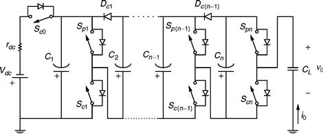
FIGURE 26.47 Circuit for applying HV-negative repetitive pulses into a capacitive load, with a negative dc power supply, Vdc.
Considering the circuit in Fig. 26.47, as the Vdc power supply is negative, it is necessary to change the topology in comparison with Fig. 26.44 in order to maintain a similar operating behavior. The two main differences are the addition of an extra switch, Sc0, which guarantees that, during the pulse period, the dc charging power supply Vdc does not participate in the pulse mode, ton. The most important regards the fact that during the charging period, T –ton, the Sci switches short circuit the load discharging any capacitance, as the one shown in Fig. 26.47.
Considering now the application of negative HV pulses into inductive loads, the circuit in Fig. 26.44 requires an additional half-bridge switching structure that connects to the load, as shown in Fig. 26.48.
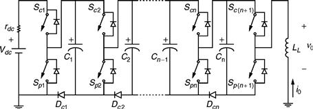
FIGURE 26.48 Circuit for applying HV-negative repetitive pulses into an inductive load.
As shown in Fig. 26.49, the operation of the circuit in Fig. 26.48 in comparison with circuit in Fig. 26.44 as some changes, which includes one additional time period for enabling the reset of the inductive load by the freewheeling diodes, tab, besides the charging, tc, and pulse modes, ton, in order to impose a zero average voltage to the load.
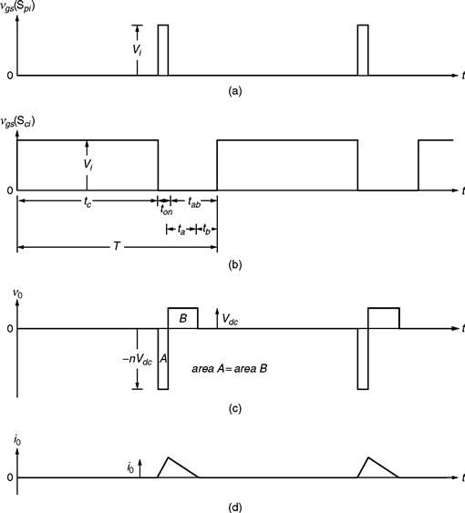
FIGURE 26.49 Theoretic waveform for the operation of the circuit in Fig. 26.48: (a) trigger signal of switches Spi, vgs(Spi) ; (b) trigger signal of switches Sci, vgs(Sci); (c) output voltage, v0 ; and (d) output current, i0.
During the charging period, the on-state of Dci and the Sp(n+ 1) antiparallel diode ensures that the output voltage, v0, applied to the load is approximately zero.
After the HV-negative pulse, ton, the Sci and Spj switches are turned off, but in order to conserve energy, the inductiveload current, i0, must have an alternative path. This path is set by freewheeling diodes (Sci antiparallel diodes and Dci diodes) and the capacitor with the lowest voltage, which is charged. Normally, Cn has the lowest voltage, thus the current path is through the Sc(n+ 1) antiparallel diode DB, capacitor Cn, and diodes Dc1 to Dcn. During this time, ta, the voltage applied to the load is, about, Vdc (voltage in capacitor Cn), resetting the inductive load. Capacitor Cn is charged until its voltage is equal to the capacitor Cn–1 voltage, after which, if there is still energy in the load, the current path changes to capacitor Cn-1. As the maximum clamping voltage is Vdc, the higher the number of stages the longer the resetting time.
In this way, most of the load magnetic energy is sent back to energy storing capacitors Ci, after which the load current i0 goes to zero and it can be imposed again the charging mode of operation. It is important to have a safety time tb in order to guarantee the completely reset of the load. Due to this load energy recovery method, the power supply energy needed to charge the capacitors after each pulse is lower, and the yield of this modulator can be higher.
EXAMPLE 26.9 A negative solid-state Marx generator needs to be assembled for delivering –9 kV, 25 µs pulses into a 900 Ω resistive load, with less than 20% voltage droop. Considering the existent equipment, there are two alternatives as follows: (1) Vdc= 1.5 kV, n = 6, and Ci=l µF; (2) Vdc=l kV, n = 9, and Ci=l µF. Determine which is the best alternative.
SOLUTION. Considering the capacitance of 1 µs in each stage, then the pulse voltage droop can be determined by (26.39). Hence, for the first alternative
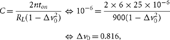
and for the second alternative
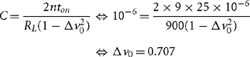
which gives, respectively, 18.35% and 29.23% voltage droop, meaning that after the pulse the capacitors stay charged with about (26.36), respectively, 1224.7 and 707.1 V. Hence, only the first alternative keeps the pulse voltage droop below 20%. In this case, the energy stored in the capacitors is (26.34) 6.75 J, three times bigger than the energy delivered to the load during each pulse (26.35) 2.25 J.
26.4.4.2 Generation of Positive Pulses
The solid-state Marx modulators for generating positive HV pulses, with different load conditions, have equivalent properties as the ones for negative pulses, shown in the previous section, besides the necessary modifications to enable the change in the output polarity. Thus, Fig. 26.50 shows the basic topology of the SM, with n stages, able to deliver positive high-voltage repetitive pulses into resistive and capacitive loads, RlCl.
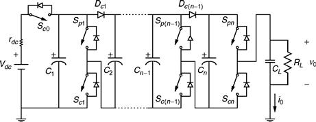
FIGURE 26.50 Circuit for applying HV-positive repetitive pulses into resistive and capacitive loads.
During the pulse mode, ton, the switches Sci and Spi are, respectively, turned off and turned on. Capacitors Ci are connected in series and their voltage applied to the load. The load voltage vq, is proportional to the charging power supply,
(26.41) ![]()
where n is the number of stages, and k < 1 characterizes the nonideal behavior of the passive and active elements in the circuit and operating conditions. Also, in this topology, for example, if Spn is off during pulse mode, the antiparallel Scn diode conducts and short circuits the last stage, imposing an output voltage of
(26.42) ![]()
Actually, the Fig. 26.50 circuit is equivalent to Fig. 26.44 circuit, whereas in this case, with a positive Vdc power supply, it can produce positive HV pulses for both resistive and capacitive loads. The capacitive load can be driven, given that during the charging mode of capacitors Ci, the load is short circuited by the Sci switches, stray inductances limiting the discharge rate.
Considering now the application of positive HV pulses into inductive loads, the circuit in Fig. 26.50 requires an additional switch Sp0 and diode D0 at the input, as shown in Fig. 26.51.
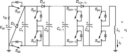
FIGURE 26.51 Circuit for applying HV-positive repetitive pulses into an inductive load.
The circuit operation requires, also, an additional time period for resetting the inductive load by the added freewheeling diodes, tab, in addition to the charging, tc, and pulse modes, ton, in order to impose a zero average voltage to the load.
Considering an inductive load, after the HV-positive pulse, the Sci and Spi switches are off, and the path for the inductive current i0 is set by the capacitor Cn, which usually has the lowest voltage, the Sci antiparallel diode and diode DB. During this time, the voltage applied to the load is approximately –Vdc (the voltage in capacitor Cn), resetting the inductive load. After the load current i0 goes to zero, the charging mode of operation can be imposed.
26.4.5 Solid-State Marx Based High-Voltage Switches
The solid-state Marx generator concept described in the previous section can be used for distributing the voltage in series-stacked semiconductors. Further, the Marx generator circuit can be used as a series switch, maintaining some intrinsic properties, which are desirable for the use with relatively low-voltage semiconductors, such as equal voltage distribution between stages and the fact the semiconductors in each stage hold-off only the stage voltage capacitor.
The Marx series switch, based on the solid-state Marx of Fig. 26.50, for positive voltages, is shown in Fig. 26.52 not to apply voltage but to hold it between its terminals. Therefore, the input power supply Vdc is removed and the Spi• switches are replaced by diodes Dpi. Also, resistors Rci are connected in parallel with the Dci diodes in order to equalize the voltage in the capacitors Ci.
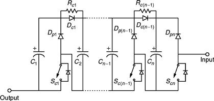
FIGURE 26.52 Series switch for positive voltages based on the Marx concept.
Consider the common HV pulse power topology of Fig. 26.53, where switches S1 and S2 commutate alternately. A HV power supply, Vdc, charges an energy storage capacitor Cdc, with current limited by resistor Rdc. The switch S1 applies the capacitor Cdc voltage vc to the capacitive load CL//RL, during the pulse period, ton. Subsequently, switch S2 discharges the load and other circuit parasitic capacitances to zero.
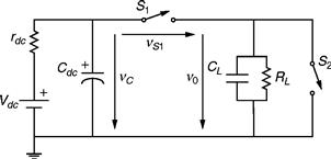
FIGURE 26.53 Proposed pulsed power HV topology for describing the operation of the series switch of Fig. 26.52.
Taking into account the proposed operating scheme, each switch Si, where i ε {1, 2}, holds a maximum voltage equal to the power supply voltage amplitude, Vdc, considering that the capacitor Cdc is charged with the voltage Vdc. When S1 is conducting, S2 holds off the voltage Vdc, and when S2 is conducting, S1 holds off the voltage Vdc. Hence, if the voltage Vdc is greater than a couple of kilo volt, a solid-state switch comprising series-stacked semiconductors is mandatory for implementing switches S1 and S2.
The switching frequency of S1 and S2 and the pulse on time depend on the energy stored in the Cdc capacitor, on the load consumption and on the power dissipated in the switches during commutation.
The proposed pulsed power topology in Fig. 26.53 implemented with the series switch of Fig. 26.52 as series switch S1 (Marx 1) and S2 (Marx 2) is shown in Fig. 26.54.
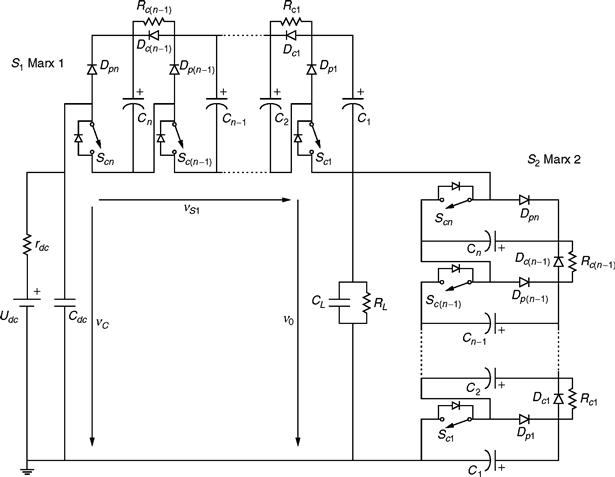
FIGURE 26.54 Proposed pulsed power topology for testing the new series switches.
The operation of Fig. 26.54 circuit can be understood considering the concept presented in Fig. 26.52 and the voltage waveforms presented in Fig. 26.56. For the first operating mode, during time ton, the Sci switches in Marx 1 are on, the Ci capacitors in Marx 1 are in parallel, and the Sci switches in Marx 2 are off, as shown in Fig. 26.55a. The capacitor Cdc voltage, vc, is applied into the load, v0, and the Ci capacitors in Marx 2 are stacked in series, through the Dpi diodes, distributing the voltage across the Sci, switches, in parallel with the load.
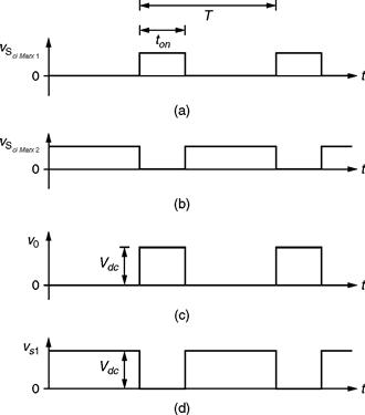
FIGURE 26.56 Theoretical waveforms for Fig. 26.54 circuit operation: (a) Marx 1 Sci drive signal; (b) Marx 2 Sci drive signal; (c) load voltage, v0; and (d) Marx 1 voltage, vs1.
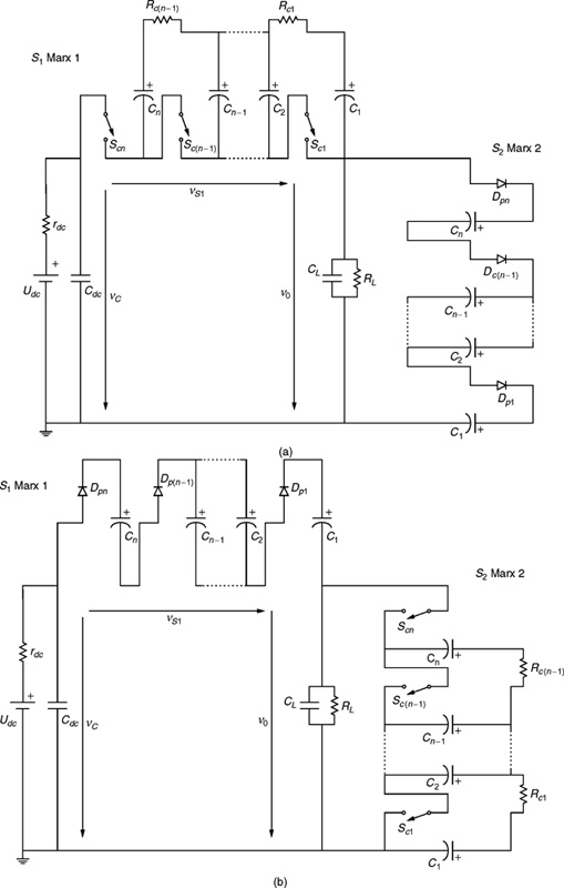
FIGURE 26.55 Operating modes for the Fig. 26.54 circuit: (a) voltage applied to the load and (b) load discharge.
Subsequently, in the second operating mode, during time T –ton, the Sci switches in Marx 1 are off and the Sci switches in Marx 2 are on, and the load is discharged to zero, as shown in Fig. 26.55b. The vc voltage appears between the Marx 1 terminals as shown in Fig. 26.56d, where this voltage is sustained by the Ci capacitors in series through the Dpi diodes, distributing the voltage across the Sci switches.
Unlike in a typical Marx generator, the Ci capacitors in both Marx 1 and Marx 2 of Fig. 26.54 can suffer from voltage imbalance problems due to the fact that the Ci capacitors are charged in series: (1) in Marx 1 during period T –ton, when the load is short-circuited and the voltage vc appears between the Marx 1 terminals, vS1; (2) in Marx 2 during period ton, when the voltage is applied to the load and the voltage vC appears between the Marx 2 terminals.
Two main causes contribute to this voltage imbalance: (1) the Ci capacitances values are not equal; (2) the Ci capacitors placed near the Vdc power supply are charged with a higher voltage due to the voltage droop in the semiconductors in each stage. Considering the later, the Dci diodes do not conduct and Rci are used in parallel to uniformly distribute the voltage between the Ci capacitors during: (1) ton in the Marx 1 switch; (2) T –ton in Marx 2 switch. Alternatively, extra switches can be placed in antiparallel with diodes Dci.
26.5 Conclusions and Future Trends
This chapter reviewed some of the most typical semiconductors and topologies used for generating repetitive unipolar and bipolar high-voltage pulses based on semiconductor devices for various load conditions. These topologies have in common the techniques for limiting the high-voltage stress onto the power semiconductor switches, still relatively low-voltage devices, considering the dozens of kilovolt needed for the pulse power applications. Techniques spread from the series (and parallel) stacks of semiconductors switches, to generalized cascodes, passing through the modified dc–dc isolated converters for pulse generation, and their cascade association, to the Marx-type solid-state generators topologies.
With semiconductor-based generators, pulse power applications have expanded into many new fields such as material modification, environment protection, and biological and medical developments. The presented topologies can bring a completely new extent of capability in repetition rate, efficiency, lifetime, compactness, and portability.
In addition to the methods to generate high-voltage pulse, the performances of the semiconductor switches determine the performance of the pulse power generators. In this way, power semiconductor devices have made significant progress in both power capability and operation speed. Various semiconductor switching units have become commercially available and have been used in various pulse power applications. The most typical devices such as SOS diodes, GTOs, IGBTs MOSFETs, and the emerging devices like SITh based on Sior SiC technology, the SiC devices such as JFETs, and cascade JFET devices were described. As the performance of these devices continues to improve, it is expected they will replace the more conventional switching devices for high-voltage applications.
State-of-the-art HV pulse generators must use several stages to obtain the desired final high-voltage pulse: the first stage can use SCRs and start at 1–2 kV, then and intermediate full-bridge resonant stage using IGBTs, or full-bridge associations, can boost this voltage to 4–10 kV, which is applied to HV high-frequency or high-pulse transformers to obtain 50–100 kV in the secondary. Diode polyphase rectifiers in the transformer secondary windings, or saturated pulse transformers, can boost the voltage roughly to 300 kV. If needed, a final stage using a SOS or SAS diode can boost the voltage up to 1 MV. Alternatively, other solutions such as solid-state Marx generators are being used, each Marx cell operating at 2–10 kV (using series stacks if needed). The required number of Marx cells should be minimized and arranged in shielded groups, the groups being connected to obtain the full HV generator. Droop voltage control and simulation are necessary to be able to design a practical HV pulse generator.
The future of solid-state pulse power is linked to the capability of making semiconductor-based high-voltage generators with superior properties in compactness, low weight, low cost, high efficiency, modularity, and very important portability to deal with future applications near the consumer.
REFERENCES
1. Kristiansen M. Pulsed Power Applications. In: Proc. IEEE International Pulsed Power Conf.. 1993: 6–10.
2. Levy S et al. Commercial Applications for Modulators and Pulse Power Technology. In: Proc. IEEE Power Modulator Symp.. 1992: 8–14.
3. Schamiloglu E. Scanning the Technology. Proc. IEEE. July 2004; vol. 92(no. 7):1014–1020.
4. Jiang W et al. Compact Solid-State Switched Pulsed Power and Its Applications. Proc. IEEE. July 2004; vol. 92(no. 7):1180–1196.
5. Akiyama H, Sakai S, Sakugawa T, Namihira T. Environmental Applications of Repetitive Pulsed Power. IEEE Trans. Dielectrics and Electrical Insulation. August 2007; vol. 14(no. 4):825–833.
6. Schoenbach KH et al. Ultrashort Electrical Pulses Open a New Gateway Into Biological Cells. Proc. IEEE. July 2004; vol. 92(no. 7):1122–1137.
7. Raso-Pueyo J, Heinz V. Pulsed Electric Fields Technology for the Food Industry - Fundamentals and Applications. 1st ed. USA: Springer; 2006.
8. Daehn GS. ASM Handbook, Volume 14B, Metalworking: Sheet Forming. USA: ASM International; 2006.
9. Neau EL. Environmental and Industrial Applications of Pulsed Power Systems. IEEE Trans. Plasma Science. February 1994; vol. 22(no. 1):2–10.
10. Fernando Silva J. Electrónica Industrial, Fundação Calouste Gulbenkian. 1st ed. Portugal: Fundacão Calouste Gulbenkian; 1998.
11. Mohan N, Undeland T, Robbins W. Power Electronics: Converters, Applications and Design. 2nd ed. USA: Jonh Wiley & Sons; 1995.
12. Mankowski J, Kristiansen M. A Review of Short Pulse Generator Technology. IEEE Trans. Plasma Science. February 2000; vol. 2(no. 1):102–108.
13. Rashid MH, ed. Power Electronics Handbook. San Diego, CA: Academic Press, Elsevier; 2007: 1172. [ISBN 13:978-0-12-088479-7, ISBN 10:0-12-088479-8].
14. Baker RJ, Johnson BP. Applying The Marx Bank Circuit Configuration To Power Mosfets. Electronics Letters. January 1993; vol. 29(no. 1):56–57.
15. Baker RJ, Ward ST. Designing nanosecond high voltage pulse generators using power MOSFETs. Electronics Letters. September 1994; vol. 30(no. 20):1634–1635.
16. Burkhart C et al. ILC Marx Modulator Development Program Status. In: Presented in Linear Accelerator Conf.. 29 September 2008.
17. Cook EG. Review of Solid-State Modulators. In: Presented at the XX International Linac Conf.. August 2000: 21–25.
18. Welleman A, Waldmeyer J, Ramezani E. Solid State Switches For Pulse Power Modulators. In: Proc. Linear Particle Accelerator Conf.. 2002: 707–709.
19. Leyh G. Prototype Development Progress toward a 500 kV Solid State Marx Modulator. In: Proc. IEEE Power Electronics Specialists Conf.. 2004: 831–834.
20. Kim J, Min B, Shenderey S, Rim G. High Voltage Marx Generator Implementation using IGBT Stacks. IEEE Trans. Dielectrics and Electrical Insulation. August 2007; vol. 14(no. 4):931–936.
21. Wu Y, Liu K, Qiu J, Liu X, Xiao H. Repetitive and high voltage Marx generator using solid-state devices. IEEE Trans. Dielectrics and Electrical Insulation. August 2007; vol. 14(no. 4):937–940.
22. Fernando Silva J, Pinto S. Control Methods for Switching Power Converters. In: Rashid MH, ed. Power Electronics Handbook. San Diego, CA: Academic Press, Elsevier; 2007: 935–998. [Chapter 34, 1172 pp, ISBN 13:978-0-12-088479-7, ISBN 10:0-12-088479-8].
23. Kempkes MA, Casey JA, Gaudreau MPJ, Hawkey TA, Roth IS. Solid-state Modulators for Commercial Pulsed Power Systems. In: Proc. IEEE International Power Modulator Symposium and High Voltage Work. 2002: 689–693.
24. Pelletier J, Anders A. Plasma-Based Ion Implantation and Deposition: A review of Physics, Technology and Applications. IEEE Trans. Plasma Science. December 2005; vol. 33(no. 6):1944–1959.
25. Smulders EHWM, Van Heesch BEJM, Van Paasen SSVB. Pulsed power corona discharges for air pollution control. IEEE Trans. Plasma Science. October 1998; vol. 26(no. 5):1476–1484.
26. Meriched A, Féliachi M, Mohellebi H. Electromagnetic Forming of Thin Metal Sheets. IEEE Trans. Magnetics. July 2000; vol. 36(no. 4):1808–1811.
27. Redondo LM, Fernando Silva J, Margato E. Analysis of a modular generator for high-voltage, high-frequency pulsed applications, using low voltage semiconductors (¡1 kV) and series connected step-up (1: 10) transformers. Review of Scientific Instruments. March 2007; vol. 78(no. 3):034702.
28. Jim Lux’s Web Site. High-Voltage, High Voltage Resistors, Water Resistance. 2003; http://home.earthlink.net/~jimlux/hv/rwater.htm .
29. Brutscher J. A 100 kV 10 A high voltage pulse generator for plasma immersion ion implantation. Review of Scientific Instruments. July 1996; vol. 67(no. 7):2621–2625.
30. Anders A, Goebel DM. Pulse Technology. In: Anders A, ed. Handbook of Plasma Immersion Ion Implantation & Deposition. USA: John Wiley & Sons; 2000. [Chapter 8].
31. Wang C, Zhang QH. EMI and its elimination in an integrated high voltage (12 kV) pulse generator. In: Proc. IEEE Industrial Electronics Society Conf.. 2000: 1044–1049.
32. Redondo LM, Margato E, Fernando Silva J. A new method to build a high-voltage pulse supply using only semiconductor switches for plasma-immersion ion implantation. Surface and Coatings Technology. 2001; vol. 136(Issues 1–3):51–54.
33. Tian X, Wang X, Tang B, Chu PK, Ko PK, Cheng YC. Special modulator for high frequency, low-voltage plasma immersion ion implantation. Review of Scientific Instruments. 1999; vol. 70(no. 3):1824–1828.
34. Wang F, Kuthi A, Jiang C, Zhou Q, Gundersen M. Flyback resonant charger for high repetition rate pseudospark pulse generator. In: Proc. IEEE International Power Modulator Symposium Conf.. 2004: 85–88.
35. Giesselman M, Heeren T. Rapid Capacitor Charger. In: Proc. IEEE International Power Modulator Symposium Conf.. 2002: 146–149.
36. Petr R, Reilly D, Freshman J, Orozco N, Pham D, Ngo L, Mangano J. Solid-state pulsed power for driving a high-power dense plasma focus x-ray source. Review of Scientific Instruments. 2000;vo. 71(no. 3):1360–1362.
37. Jiang W et al. Development of Repetitive Pulsed Power Generators using Power Semiconductor Devices. In: Proc. IEEE International Symposium on Power Semiconductor Devices and ICs. 2005: 1167–1172.
38. Gaudreau MPJ, Hawkey T, Petry J, Kempkes M. A solid state pulsed power system for food processing. In: 2001: 1174–1177. Proc. IEEE Pulsed Power and Plasma Science; vol. 2.
39. Welleman A, Fleischmann W, Kaesler W. Solid state on-off switches using IGCT technology. In: Proc. IEEE Pulsed Power and Plasma Science Conf.. 2007: 1025–1028.
40. Jiang W. Fast High Voltage Switching Using Stacked MOSFETs. IEEE Trans. Dielectrics and Electrical Insulation. 2007; vol. 14(no. 4):947–950.
41. Kim J, Min B, Shenderey S, Rim G-H. High Voltage Pulsed Power Supply Using IGBT Stacks. IEEE Trans. Dielectrics and Electrical Insulation. 2007; vol. 14(no. 4):921–926.
42. Williams BW. Series and Parallel Device Operation, Protection, and Interference. In: Williams BW, ed. Power Electronics. UK: Barry W Williams; 2005. [Chapter 10].
43. Gunturi S, Assal J, Schneider D, Eicher S. Innovative Metal System for IGBT Press Pack Modules. In: Proc. Int. Symp. Power Semiconductor Devices and ICs. 2003: 110–113.
44. Goebel DM. Pulse Technology. In: Anders A, ed. Handbook of Plasma Immersion Ion Implantation & Deposition. USA: John Wiley & Sons; 2000. [Chapter 8].
45. Redondo LM, Silva JF, Margato E. Pulse shape improvement in core-type high-voltage pulse transformers with auxiliary windings. IEEE Transactions on Magnetics. May 2007; vol. 43(no. 5):1973–1982.
46. Lord HW. Pulse transformers. IEEE Transactions on Magnetics. March 1971; vol. 7(no. 1):17–28.
47. Ranon PM. Compact pulsed transformer power conditioning system for generating high voltage, high energy, rapid rise time pulses. IEEE Transactions on Magnetics. January 1989; vol. 25(no. 1):480–484.
48. Rashid MH. Power Electronics: Circuits, Devices and Applications. Englewood Cliffs, NJ: Prentice Hall; 2003.
49. Leu CS, Hua G, Lee FC, Zhou C. Analysis and design of a R-C-D clamp Forward converter. In: Proc. High Frequency Power Conversion Conf.. 1992: 198–208.
50. Redondo LM, Fernando Silva J. Flyback versus Forward switching power supply topologies for unipolar pulsed power applications. IEEE Trans. Plasma Science. January 2009; vol. 37(no. 1):171–178.
51. Klein J, Padberg M. A modular low-cost, high-voltage pulse generator that is highly effective in terms of pulse energy and repetition frequency. Measurement Science and Technology. May 1995; vol. 6(no. 5):550–555.
52. Tian X, Wang X, Tang B, Chu PK, Ko PK, Cheng YC. Special modulator for high frequency, low-voltage plasma immersion ion implantation. Review of Scientific Instruments. March 1999; vol. 70(no. 3):1824–1828.
53. Smith W. Transient Electronics - Pulsed Circuit Technology. Chichester, UK: Wiley; 2002.
54. Kostenko M, Piotrovski L. Electrical Machines. Rev ed. London, UK: Central Books Ltd; 1980.
55. Willis WL. Pulse-Voltage Circuits. In: Dollinger RE, Sarjeant WJ, eds. High Power electronics. Blue Ridge Summit, PA: Tab Books Inc.; 1989. [Chapter 3].
56. Gregory K, Stevenson P, Burke R. Four-stage Marx generator using thyristors. Review of Scientific Instruments. November 1998; vol. 69(no. 11):3996–3997.
57. Wu Y, Liu K, Qiu J, Liu X, Xiao H. Repetitive and high voltage Marx generator using solid-state devices. IEEE Trans. Dielectrics and Electrical Insulation. 2007; vol. 14(no. 4):937–940.
58. Cassel RL. An all solid state pulsed Marx type modulator for Magnetrons and Klystrons. In: Proc. IEEE International Power Modulator Conf.. 2004: 836–838.
59. Redondo LM, Fernando Silva J. Repetitive high-voltage solid-state Marx modulator design for various load conditions. IEEE Trans. Plasma Science. 2009; vol. 37(no. 8):1632–1637.
60. Keith WD, Pringle D, Rice P, Birke PV. Distributed magnetic coupling synchronizes a stacked 25-kV MOSFET switch. IEEE Trans. Power Electronics. January 2000; vol. 15(no. 1):58–61.