
12
Three-phase Controlled Rectifiers
Department of Electrical Engineering, Pontificia Universidad Católica de Chile Vicuña Mackenna 4860, Santiago, Chile
12.1 Introduction
12.2 Line-commutated Controlled Rectifiers
12.2.1 Three-phase Half-wave Rectifier
12.2.2 Six-pulse or Double Star Rectifier
12.2.3 Double Star Rectifier with Interphase Connection
12.2.4 Three-phase Full-wave Rectifier or Graetz Bridge
12.2.5 Half Controlled Bridge Converter
12.2.6 Commutation
12.2.7 Power Factor
12.2.8 Harmonic Distortion
12.2.9 Special Configurations for Harmonic Reduction
12.2.10 Applications of Line-commutated Rectifiers in Machine Drives
12.2.11 Applications in HVDC Power Transmission
12.2.12 Dual Converters
12.2.13 Cycloconverters
12.1 Introduction
Three-phase controlled rectifiers have a wide range of applications, from small rectifiers to large high voltage direct current (HVDC) transmission systems. They are used for electrochemical processes, many kinds of motor drives, traction equipment, controlled power supplies and many other applications. From the point of view of the commutation process, they can be classified into two important categories: line-commutated controlled rectifiers (thyristor rectifiers) and force-commutated pulse width modulated (PWM) rectifiers.
12.2 Line-commutated Controlled Rectifiers
12.2.1 Three-phase Half-wave Rectifier
Figure 12.1 shows the three-phase half-wave rectifier topology. To control the load voltage, the half-wave rectifier uses three common-cathode thyristor arrangement. In this figure, the power supply and the transformer are assumed ideal. The thyristor will conduct (ON state), when the anode-to-cathode voltage vAK is positive and a firing current pulse iG is applied to the gate terminal. Delaying the firing pulse by an angle α controls the load voltage. As shown in Fig. 12.2, the firing angle α is measured from the crossing point between the phase supply voltages. At that point, the anode-to-cathode thyristor voltage vAK begins to be positive. Figure 12.3 shows that the possible range for gating delay is between α = 0° and α = 180°, but because of commutation problems in actual situations, the maximum firing angle is limited to around 160°. As shown in Fig. 12.4, when the load is resistive, current id has the same waveform of the load voltage. As the load becomes more and more inductive, the current flattens and finally becomes constant. The thyristor goes to the non-conducting condition (OFF state) when the following thyristor is switched ON, or the current, tries to reach a negative value.

FIGURE 12.1 Three-phase half-wave rectifier.

FIGURE 12.2 Instantaneous dc voltage vD, average dc voltage VD, and firing angle α.

FIGURE 12.3 Possible range for gating delay in angle α.

FIGURE 12.4 DC current waveforms.
With the help of Fig. 12.2, the load average voltage can be evaluated, and is given by:
 (12.1)
where VMAX is the secondary phase-to-neutral peak voltage, Vrmsf-N its root mean square (rms) value and ω is the angular frequency of the main power supply. It can be seen from Eq. (12.1) that the load average voltage VD is modified by changing firing angle α. When α < 90°, VD is positive and when α > 90°, the average dc voltage becomes negative. In such a case, the rectifier begins to work as an inverter and the load needs to be able to generate power reversal by reversing its dc voltage.
The ac currents of the half-wave rectifier are shown in Fig. 12.5. This drawing assumes that the dc current is constant (very large LD). Disregarding commutation overlap, each valve conducts during 120° per period. The secondary currents (and thyristor currents) present a dc component that is undesirable, and makes this rectifier not useful for high power applications. The primary currents show the same waveform, but with the dc component removed. This very distorted waveform requires an input filter to reduce harmonics contamination.

FIGURE 12.5 AC current waveforms for the half-wave rectifier.
The current waveforms shown in Fig. 12.5 are useful for designing the power transformer. Starting from:
 (12.2)
where VAprime and VAsec are the ratings of the transformer for the primary and secondary side respectively. Here PD is the power transferred to the dc side. The maximum power transfer is with α = 0° (or α = 180°). Then, to establish a relation between ac and dc voltages, Eq. (12.1) for α = 0° is required:
![]() (12.3)
(12.3)
and:
![]() (12.4)
(12.4)
where a is the secondary to primary turn relation of the transformer. On the other hand, a relation between the currents is also possible to obtain. With the help of Fig. 12.5:
![]() (12.5)
(12.5)
Combining Eqs. (12.2) to (12.6), it yields:
 (12.7)
Equation (12.7) shows that the power transformer has to be oversized 21% at the primary side, and 48% at the secondary side. Then, a special transformer has to be built for this rectifier. In terms of average VA, the transformer needs to be 35% larger that the rating of the dc load. The larger rating of the secondary with respect to primary is because the secondary carries a dc component inside the windings. Furthermore, the transformer is oversized because the circulation of current harmonics does not generate active power. Core saturation, due to the dc components inside the secondary windings, also needs and its average value is given by: to be taken in account for iron oversizing.
12.2.2 Six-pulse or Double Star Rectifier
The thyristor side windings of the transformer shown in Fig. 12.6 form a six-phase system, resulting in a six-pulse starpoint (midpoint connection). Disregarding commutation overlap, each valve conducts only during 60° per period. The direct voltage is higher than that from the half-wave rectifier and its average value is given by:

FIGURE 12.6 Six-pulse rectifier.
 (12.8)
The dc voltage ripple is also smaller than the one generated by the half-wave rectifier, due to the absence of the third harmonic with its inherently high amplitude. The smoothing reactor LD is also considerably smaller than the one needed for a three-pulse (half-wave) rectifier.
The ac currents of the six-pulse rectifier are shown in Fig. 12.7. The currents in the secondary windings present a dc component, but the magnetic flux is compensated by the double star. As can be observed, only one valve is fired at a time and then this connection in no way corresponds to a parallel connection. The currents inside the delta show a symmetrical waveform with 60° conduction. Finally, due to the particular transformer connection shown in Fig. 12.6, the source currents also show a symmetrical waveform, but with 120° conduction.

FIGURE 12.7 AC current waveforms for the six-pulse rectifier.
Evaluation of the the rating of the transformer is done in similar fashion to the way the half-wave rectifier is evaluated:
 (12.9)
Thus the transformer must be oversized 28% at the primary side and 81% at the secondary side. In terms of size it has an average apparent power of 1.55 times the power PD (55% oversized). Because of the short conducting period of the valves, the transformer is not particularly well utilized.
12.2.3 Double Star Rectifier with Interphase Connection
This topology works as two half-wave rectifiers in parallel, and is very useful when high dc current is required. An optimal way to reach both good balance and elimination of harmonics is through the connection shown in Fig. 12.8. The two rectifiers are shifted by 180°, and their secondary neutrals are connected through a middle-point autotransformer called “interphase transformer.” The interphase transformer is connected between the two secondary neutrals and the middle point at the load return. In this way, both groups operate in parallel. Half the direct current flows in each half of the interphase transformer, and then its iron core does not become saturated. The potential of each neutral can oscillate independently, generating an almost triangular voltage waveform (VT) in the interphase transformer, as shown in Fig. 12.9. As this converter work like two half-wave rectifiers connected in parallel, the load average voltage is the same as in Eq. (12.1):

FIGURE 12.8 Double star rectifier with interphase transformer.

FIGURE 12.9 Operation of the interphase connection for α = 0°.
![]() (12.10)
(12.10)
where Vrmsf–N is the phase-to-neutral rms voltage at the valve side of the transformer (secondary).
The Fig. 12.9 also shows the two half-wave rectifier voltages, related to their respective neutrals. Voltage vD1 represents the potential between the common cathode connection and the neutral N1. The voltage vD2 is between the common cathode connection and N2. It can be seen that the two instantaneous voltages are shifted, which gives as a result, a voltage vp that is smoother than vD1 and vD2
Figure 12.10 shows how vD vD1, VD2, and VT change when the firing angle changes from α = 0° to 180°.

FIGURE 12.10 Firing angle variation from α = 0° to 180°.
The transformer rating in this case is:
 (12.11)
And the average rating power will be 1.26 PD which is better than the previous rectifiers (1.35 for the half-wave rectifier and 1.55 for the six-pulse rectifier). Thus the transformer is well utilized. Figure 12.11 shows ac current waveforms for a rectifier with interphase transformer.

FIGURE 12.11 AC current waveforms for the rectifier with interphase transformer.
12.2.4 Three-phase Full-wave Rectifier or Graetz Bridge
Parallel connection via interphase transformers permits the implementation of rectifiers for high current applications. Series connection for high voltage is also possible, as shown in the full-wave rectifier of Fig. 12.12. With this arrangement, it can be seen that the three common cathode valves generate a positive voltage with respect to the neutral, and the three common anode valves produce a negative voltage. The result is a dc voltage, twice the value of the half-wave rectifier. Each half of the bridge is a three-pulse converter group. This bridge connection is a two-way connection and alternating currents flow in the valve-side transformer windings during both half periods, avoiding dc components into the windings, and saturation in the transformer magnetic core. These characteristics make the so-called Graetz bridge the most widely used line-commutated thyristor rectifier. The configuration does not need any special transformer and works as a six-pulse rectifier. The series characteristic of this rectifier produces a dc voltage twice the value of the half-wave rectifier. The load average voltage is given by:

FIGURE 12.12 Three-phase fall-wave rectifier or Graetz bridge.
 (12.12)
![]() (12.13)
(12.13)
where VMAX is the peak phase-to-neutral voltage at the secondary transformer terminals, Vrmsf–N its rms value, and Vsecf–f the rms phase-to-phase secondary voltage, at the valve terminals of the rectifier.
Figure 12.13 shows the voltages of each half-wave bridge of this topology, vposD and vnegD, the total instantaneous dc voltage vD, and the anode-to-cathode voltage vAK in one of the bridge thyristors. The maximum value of vak is ![]() 3 VMAXwhich is the same as that of the half-wave converter and the interphase transformer rectifier. The double star rectifier presents a maximum anode-to-cathode voltage of two times VMAX Figure 12.14 shows the currents of the rectifier, which assumes that LD is large enough to keep the dc current smooth. The example is for the same ΔY transformer connection shown in the topology of Fig. 12.12. It can be noted that the secondary currents do not carry any dc component, thereby avoiding overdesign of the windings and transformer saturation. These two figures have been drawn for a firing angle, α of approximately 30°. The perfect symmetry of the currents in all windings and lines is one of the reasons why this rectifier is the most popular of its type. The transformer rating in this case is
3 VMAXwhich is the same as that of the half-wave converter and the interphase transformer rectifier. The double star rectifier presents a maximum anode-to-cathode voltage of two times VMAX Figure 12.14 shows the currents of the rectifier, which assumes that LD is large enough to keep the dc current smooth. The example is for the same ΔY transformer connection shown in the topology of Fig. 12.12. It can be noted that the secondary currents do not carry any dc component, thereby avoiding overdesign of the windings and transformer saturation. These two figures have been drawn for a firing angle, α of approximately 30°. The perfect symmetry of the currents in all windings and lines is one of the reasons why this rectifier is the most popular of its type. The transformer rating in this case is

FIGURE 12.13 Voltage waveforms for the Graetz bridge.

FIGURE 12.14 Current waveforms for the Graetz bridge.
 (12.14)
As can be noted, the transformer needs to be oversized only 5%, and both primary and secondary windings have the same rating. Again, this value can be compared with the previous rectifier transformers: 1.35PD for the half-wave rectifier, 1.55 PD for the six-pulse rectifier, and 1.26 PD for the interphase transformer rectifier. The Graetz bridge makes excellent use of the power transformer.
12.2.5 Half Controlled Bridge Converter
The fully controlled three-phase bridge converter shown in Fig. 12.12 has six thyristors. As already explained here, this circuit operates as a rectifier when each thyristor has a firing angle α < 90° and functions as an inverter for α > 90°. If inverter operation is not required, the circuit may be simplified by replacing three controlled rectifiers with power diodes, as in Fig. 12.15a. This simplification is economically attractive because diodes are considerably less expensive than thyristors and they do not require firing angle control electronics.
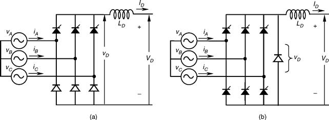
FIGURE 12.15 One-quadrant bridge converter circuits: (a) half-controlled bridge and (b) free-wheeling diode bridge.
The half controlled bridge, or “semiconverter,” is analyzed by considering it as a phase-controlled half-wave circuit in series with an uncontrolled half-wave rectifier. The average dc voltage is given by the following equation
![]() (12.15)
(12.15)
Then, the average voltage VD; never reaches negative values. The output voltage waveforms of half-controlled bridge are similar to those of a fully controlled bridge with a freewheeling diode. The advantage of the free-wheeling diode connection, shown in Fig. 12.15b is that there is always a path for the dc current, independent of the status of the ac line and of the converter. This can be important if the load is inductive–resistive with a large time constant, and there is an interruption in one or more of the line phases. In such a case, the load current could commutate to the free-wheeling diode.
12.2.6 Commutation
The description of the converters in the previous sections was based upon assumption that the commutation was instantaneous. In practice this is not possible, because the transfer of current between two consecutive valves in a commutation group takes a finite time. This time, called overlap time, depends on the phase-to-phase voltage between the valves participating in the commutation process, and the line inductance Ls between the converter and power supply. During the overlap time, two valves conduct, and the phase-to-phase voltage drops entirely on the inductances Ls. Assuming the dc current ID to be smooth and with the help of Fig. 12.16, the following relation is deduced

FIGURE 12.16 Commutation process.
![]() (12.16)
(12.16)
where isc is the current in the valve being fired during the commutation process (thyristor T2 in Fig. 12.16). This current can be evaluated, and it yields
![]() (12.17)
(12.17)
The constant “C” is evaluated through initial conditions at the instant when T2 is ignited. In terms of angle, when ωt = α
 (12.18)
Replacing Eq. (12.18) in (12.17):
![]() (12.19)
(12.19)
Before commutation, the current ID was carried by thyristor T1 (see Fig. 12.16). During the commutation time, the load current ID remains constant, isc returns through T1, and T1 is automatically switched off when the current isc reaches the value of ID. This happens because thyristors cannot conduct in reverse direction. At this moment, the overlap time lasts and the current ID is then conducted by T2. In terms of angle, when ωt = α + μ, isc = ID, where μ is defined as the “overlap angle.” Replacing this final condition in Eq. (12.19) yields
![]() (12.20)
(12.20)
To avoid confusion in a real analysis, it has to be remembered that Vf-f corresponds to the secondary voltage in case of transformer utilization. For this reason, the abbreviation “sec” has been added to the phase-to-phase voltage in Eq. (12.20).
During commutation, two valves conduct at a time, which means that there is an instantaneous short circuit between the two voltages participating in the process. As the inductances of each phase are the same, the current isc produces the same voltage drop in each Ls, but with opposite sign because this current flows in reverse direction and with opposite slope in each inductance. The phase with the higher instantaneous voltage suffers a voltage drop Δv and the phase with the lower voltage suffers a voltage increase +Δv. This situation affects the dc cvoltage VC, reducing its value an amount ΔVmed. Figure 12.17 shows the meanings of Δv, ΔVmed, μ, and isc.

FIGURE 12.17 Effect of the overlap angle on the voltages and currents.
The area ΔVmed showed in Fig. 12.17, represents the loss of voltage that affects the average voltage VC, and can be evaluated through the integration of Δv during the overlap angle μ. The voltage drop Δv can be expressed as
 (12.21)
Integrating Eq. (12.21) into the corresponding period (60°) and interval (μ) and starting at the instant when the commutation begins (α)
 (12.22)
Subtracting ΔVmed in Eq. (12.13)
![]() (12.24)
(12.24)
or
![]() (12.26)
(12.26)
Equations (12.20) and (12.25) can be written as a function of the primary winding of the transformer, if there is any transformer.
 (12.27)
where a = Vsecf–f/Vprimf–f. With Eqs. (12.27) and (12.28) one gets
![]() (12.29)
(12.29)
Equation (12.29) allows a very simple equivalent circuit of the converter to be made, as shown in Fig. 12.18. It is important to note that the equivalent resistance of this circuit is not real, because it does not dissipate power.

FIGURE 12.18 Equivalent circuit for the converter.
From the equivalent circuit, regulation curves for the rectifier under different firing angles are shown in Fig. 12.19. It should be noted that these curves correspond only to an ideal situation, but helps in understanding the effect of voltage drop Δ? on dc voltage. The commutation process and the overlap angle also affects the voltage vα and anode-to-cathode thyristor voltage, as shown in Fig. 12.20.

FIGURE 12.19 DC voltage regulation curves for rectifier operation.

FIGURE 12.20 Effect of the overlap angle on va and on thyristor voltage ?AK.
12.2.7 Power Factor
The displacement factor of the fundamental current, obtained from Fig. 12.14 is
![]() (12.30)
(12.30)
In the case of non-sinusoidal current, the active power delivered per phase by the sinusoidal supply is
![]() (12.31)
(12.31)
where Vrmsa is the rms value of the voltage va and Irmsa1 the rms value of ia1 (fundamental component of ia). Analog relations can be obtained for vb, and vc.
The apparent power per phase is given by
![]() (12.32)
(12.32)
The power factor is defined by
![]() (12.33)
(12.33)
By substituting Eqs. (12.30), (12.31), and (12.32) into Eq. (12.33), the power factor can be expressed as follows
![]() (12.34)
(12.34)
This equation shows clearly that due to the non-sinusoidal waveform of the currents, the power factor of the rectifier is negatively affected by both the firing angle α and the distortion of the input current. In effect, an increase in the distortion of the current produces an increase in the value of Irmsa in Eq. (12.34), which deteriorates the power factor.
12.2.8 Harmonic Distortion
The currents of the line-commutated rectifiers are far from being sinusoidal. For example, the currents generated from the Graetz rectifier (see Fig. 12.14b) have the following harmonic content
 (12.35)
Some of the characteristics of the currents, obtained from Eq. (12.35) include: (i) the absence of triple harmonics; (ii) the presence of harmonics of order 6k ± 1 for integer values of k; (iii) those harmonics of orders 6k + 1 are of positive sequence; (iv) those of orders 6k – 1 are of negative sequence; (v) the rms magnitude of the fundamental frequency is
![]() (12.36)
(12.36)
and (vi) the rms magnitude of the nth harmonic is
![]() (12.37)
(12.37)
If either, the primary or the secondary three-phase windings of the rectifier transformer are connected in delta, the ac side current waveforms consist of the instantaneous differences between two rectangular secondary currents 120° apart as shown in Fig. 12.14e. The resulting Fourier series for the current in phase “a” on the primary side is
 (12.38)
This series differs from that of a star connected transformer only by the sequence of rotation of harmonic orders 6k ± 1 for odd values of k, i.e. the 5th, 7th, 17th, 19th, etc.
12.2.9 Special Configurations for Harmonic Reduction
A common solution for harmonic reduction is through the connection of passive filters, which are tuned to trap a particular harmonic frequency. A typical configuration is shown in Fig. 12.21.

FIGURE 12.21 Typical passive filter for one phase.
However, harmonics also can be eliminated using special configurations of converters. For example, 12-pulse configuration consists of two sets of converters connected as shown in Fig. 12.22. The resultant ac current is given by the sum of the two Fourier series of the star connection (Eq. (12.35)) and delta connection transformers (Eq. (12.38))

FIGURE 12.22 12-pulse rectifier configuration.
 (12.39)
The series only contains harmonics of order 12k ± 1. The harmonic currents of orders 6k ± 1 (with k odd), i.e. 5th, 7th, 17th, 19th, etc. circulate between the two converter transformers but do not penetrate the ac network.
The resulting line current for the 12-pulse rectifier, shown in Fig. 12.23, is closer to a sinusoidal waveform than previous line currents. The instantaneous dc voltage is also smoother with this connection.

FIGURE 12.23 Line current for the12-pulse rectifier
Higher pulse configuration using the same principle is also possible. The 12-pulse rectifier was obtained with a 30° phase shift between the two secondary transformers. The addition of further, appropriately shifted, transformers in parallel provides the basis for increasing pulse configurations. For instance, 24-pulse operation is achieved by means of four transformers with 15° phase shift, and 48-pulse operation requires eight transformers with 7.5° phase shift (transformer connections in zig-zag configuration).
Although theoretically possible, pulse numbers above 48 are rarely justified due to the practical levels of distortion found in the supply voltage waveforms. Further, the converter topology becomes more and more complicated.
An ingenious and very simple way to reach high pulse operation is shown in Fig. 12.24. This configuration is called dc ripple reinjection. It consists of two parallel converters connected to the load through a multistep reactor. The reactor uses a chain of thyristor-controlled taps, which are connected to symmetrical points of the reactor. By firing the thyristors located at the reactor at the right time, high-pulse operation is reached. The level of pulse operation depends on the number of thyristors connected to the reactor. They multiply the basic level of operation of the two converters. The example, is Fig. 12.24, shows a 48-pulse configuration, obtained by the multiplication of basic 12-pulse operation by four reactor thyristors. This technique also can be applied to series connected bridges.

FIGURE 12.24 DC ripple reinjection technique for 48-pulse operation.
Another solution for harmonic reduction is the utilization of active power filters. Active power filters are special pulse width modulated (PWM) converters, able to generate the harmonics the converter requires. Figure 12.25 shows a current controlled shunt active power filter.

FIGURE 12.25 Current controlled shunt active power filter.
12.2.10 Applications of Line-commutated Rectifiers in Machine Drives
Important applications for line-commutated three-phase controlled rectifiers, are found in machine drives. Figure 12.26 shows a dc machine control implemented with a six-pulse rectifier. Torque and speed are controlled through the armature current ID and excitation current Iexc. Current ID is adjusted with VD, which is controlled by the firing angle α through Eq. (12.12). This dc drive can operate in two quadrants: positive and negative dc voltage. This two-quadrant operation allows regenerative braking when α > 90° and Iexc < 0.

FIGURE 12.26 DC machine drive with a six-pulse rectifier.
The converter of Fig. 12.26 can also be used to control synchronous machines, as shown in Fig. 12.27. In this case, a second converter working in the inverting mode operates the machine as self-controlled synchronous motor. With this second converter, the synchronous motor behaves like a dc motor but has none of the disadvantages of mechanical commutation. This converter is not line commutated, but machine commutated.
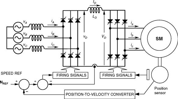
FIGURE 12.27 Self-controlled synchronous motor drive.
The nominal synchronous speed of the motor on a 50 or 60 Hz ac supply is now meaningless and the upper speed limit is determined by the mechanical limitations of the rotor construction. There is disadvantage that the rotational emfs required for load commutation of the machine side converter are not available at standstill and low speeds. In such a case, auxiliary force commutated circuits must be used.
The line-commutated rectifier controls the torque of the machine through firing angle α. This approach gives direct torque control of the commutatorless motor and is analogous to the use of armature current control shown in Fig. 12.26 for the converter-fed dc motor drive.
Line-commutated rectifiers are also used for speed control of wound rotor induction motors. Subsynchronous and supersynchronous static converter cascades using a naturally commutated dc link converter, can be implemented. Figure 12.28 shows a supersynchronous cascade for a wound rotor induction motor, using a naturally commutated dc link converter.

FIGURE 12.28 Supersynchronous cascade for a wound rotor induction motor.
In the supersynchronous cascade shown in Fig. 12.28, the right hand bridge operates at slip frequency as a rectifier or inverter, while the other operates at network frequency as an inverter or rectifier. Control is difficult near synchronism when slip frequency emfs are insufficient for natural commutation and special circuit configuration employing forced commutation or devices with a self-turn-off capability are necessary for the passage through synchronism. This kind of supersynchronous cascade works better with cycloconverters.
12.2.11 Applications in HVDC Power Transmission
High voltage direct current (HVDC) power transmission is the most powerful application for line-commutated converters that exist today. There are power converters with ratings in excess of 1000 MW. Series operation of hundreds of valves can be found in some HVDC systems. In high power and long distance applications, these systems become more economical than conventional ac systems. They also have some other advantages compared with ac systems:
1. they can link two ac systems operating unsynchronized or with different nominal frequencies, that is 50 ↔ 60 Hz;
2. they can help in stability problems related with sub-synchronous resonance in long ac lines;
3. they have very good dynamic behavior and can interrupt short-circuit problems very quickly;
4. if transmission is by submarine or underground cable, it is not practical to consider ac cable systems exceeding 50 km, but dc cable transmission systems are in service whose length is in hundreds of kilometers and even distances of 600 km or greater have been considered feasible;
5. reversal of power can be controlled electronically by means of the delay firing angles α; and
6. some existing overhead ac transmission lines cannot be increased. If overbuilt with or upgraded to dc transmission can substantially increase the power transfer capability on the existing right-of-way.
The use of HVDC systems for interconnections of asynchronous systems is an interesting application. Some continental electric power systems consist of asynchronous networks such as those for the East, West, Texas, and Quebec networks in North America, and islands loads such as that for the Island of Gotland in the Baltic Sea make good use of the HVDC interconnections.
Nearly all HVDC power converters with thyristor valves are assembled in a converter bridge of 12-pulse configuration, as shown in Fig. 12.29. Consequently, the ac voltages applied to each six-pulse valve group which makes up the 12-pulse valve group have a phase difference of 30° which is utilized to cancel the ac side, 5th and 7th harmonic currents and dc side, 6th harmonic voltage, thus resulting in a significant saving in harmonic filters.

FIGURE 12.29 Typical HVDC power system: (a) detailed circuit and (b) unilinear diagram.
Some useful relations for HVDC systems include:
![]() (12.40)
(12.40)


 (12.42)
 (12.43)
 (12.44)
![]() (12.45)
(12.45)
Fundamental secondary component of I
![]() (12.46)
(12.46)
Replacing Eq. (12.46) in (12.45)
![]() (12.47)
(12.47)
as Ip = I cos φ, it yields Fig. 12.30a
![]() (12.48)
(12.48)
b) Inverter Side:The same equations are applied for the inverter side, but the firing angle α is replaced by γ, where γ is
![]() (12.49)
(12.49)
As reactive power always goes in the converter direction, Eq. (12.44) for inverter side becomes (Fig. 12.30b)
 (12.50)

FIGURE 12.30 Definition of angle γ for inverter side: (a) rectifier side and (b) inverter side.
12.2.12 Dual Converters
In many variable-speed drives, four-quadrant operation is required, and three-phase dual converters are extensively used in applications up to 2 MW level. Figure 12.31 shows a three-phase dual converter, where two converters are connected back-to-back.

FIGURE 12.31 Dual converter in a four-quadrant dc drive.
In the dual converter, one rectifier provides the positive current to the load and the other the negative current. Due to the instantaneous voltage differences between the output voltages of the converters, a circulating current flows through the bridges. The circulating current is normally limited by circulating reactor, LD, as shown in Fig. 12.31. The two converters are controlled in such a way that if α+ is the delay angle of the positive current converter, the delay angle of the negative current converter is α− = 180° –α+.
Figure 12.32 shows the instantaneous dc voltages of each converter, v+D and v−D. Despite the average voltage VD is the same in both the converters, their instantaneous voltage differences shown as voltage vr, are producing the circulating current ir, which is superimposed with the load currents i+D and i−D.

FIGURE 12.32 Waveform of circulating current: (a) instantaneous dc voltage from positive converter: (b) instantaneous dc voltage from negative converter; and (c) voltage difference between v+D and v−D, vr, and circulating current ir.
To avoid the circulating current ir, it is possible to implement a “circulating current free” converter if a dead time of a few milliseconds is acceptable. The converter section, not required to supply current, remains fully blocked. When a current reversal is required, a logic switch-over system determines at first the instant at which the conducting converter's current becomes zero. This converter section is then blocked and the further supply of gating pulses to it is prevented. After a short safety interval (dead time), the gating pulses for the other converter section are released.
12.2.13 Cycloconverters
A different principle of frequency conversion is derived from the fact that a dual converter is able to supply an ac load with a lower frequency than the system frequency. If the control signal of the dual converter is a function of time, the output voltage will follow this signal. If this control signal value alters sinusoidally with the desired frequency, then the waveform depicted in Fig. 12.33a consists of a single-phase voltage with a large harmonic current. As shown in Fig. 12.33b, if the load is inductive, the current will present less distortion than voltage.
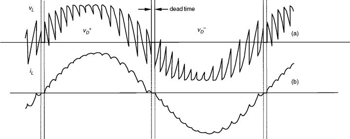
FIGURE 12.33 Cycloconverter operation: (a) voltage waveform and (b) current waveform for inductive load.
The cycloconverter operates in all four quadrants during a period. A pause (dead time) at least as small as the time required by the switch-over logic occurs after the current reaches zero, that is, between the transfer to operation in the quadrant corresponding to the other direction of current flow.
Three single-phase cycloconverters may be combined to build a three-phase cycloconverter. The three-phase cycloconverters find an application in low-frequency, high-power requirements. Control speed of large synchronous motors in the low-speed range is one of the most common applications of three-phase cycloconverters. Figure 12.34 is a diagram for this application. They are also used to control slip frequency in wound rotor induction machines, for supersynchronous cascade (Scherbius system).

FIGURE 12.34 Synchronous machine drive with a cycloconverter.
12.2.14 Harmonic Standards and Recommended Practices
In view of the proliferation of the power converter equipment connected to the utility system, various national and international agencies have been considering limits on harmonic current injection to maintain good power quality. As a consequence, various standards and guidelines have been established that specify limits on the magnitudes of harmonic currents and harmonic voltages.
The Comité Européen de Normalisation Electrotechnique (CENELEC), International Electrical Commission (IEC), and West German Standards (VDE) specify the limits on the voltages (as a percentage of the nominal voltage) at various harmonics frequencies of the utility frequency, when the equipment-generated harmonic currents are injected into a network whose impedances are specified.
According with Institute of Electrical and Electronic Engineers-519 standards (IEEE), Table 12.1 lists the limits on the harmonic currents that a user of power electronics equipment and other non-linear loads is allowed to inject into theutility system. Table 12.2 lists the quality of voltage that the utility can furnish the user.
TABLE 12.1 Harmonie current limits in percent of fundamental

TABLE 12.2 Harmonic voltage limits in percent of fundamental

In Table 12.1, the values are given at the point of connection of non-linear loads. The THD is the total harmonic distortion given by Eq. (12.51) and h is the number of the harmonic.
 (12.51)
The total current harmonic distortion allowed in Table 12.1 increases with the value of short circuit current.
The total harmonic distortion in the voltage can be calculated in a manner similar to that given by Eq. (12.51). Table 12.2 specifies the individual harmonics and the THD limits on the voltage that the utility supplies to the user at the connection point.
12.3 Force-commutated Three-phase Controlled Rectifiers
12.3.1 Basic Topologies and Characteristics
Force-commutated rectifiers are built with semiconductors with gate-turn-off capability. The gate-turn-off capability allows full control of the converter, because valves can be switched ON and OFF whenever is required. This allows the commutation of the valves, hundreds of times in one period which is not possible with line-commutated rectifiers, where thyristors are switched ON and OFF only once a cycle. This feature has the following advantages: (a) the current or voltage can be modulated (PWM), generating less harmonic contamination; (b) power factor can be controlled and even it can be made leading; and (c) they can be built as voltage source or current source rectifiers; (d) the reversal of power in thyristor rectifiers is by reversal of voltage at the dc link. Instead, force-commutated rectifiers can be implemented for both, reversal of voltage or reversal of current.
There are two ways to implement force-commutated three-phase rectifiers: (a) as a current source rectifier, where power reversal is by dc voltage reversal; and (b) as a voltage source rectifier, where power reversal is by current reversal at the dc link. Figure 12.35 shows the basic circuits for these two topologies.

FIGURE 12.35 Basic topologies for force-commutated PWM rectifiers: (a) current source rectifier and (b) voltage source rectifier.
12.3.2 Operation of the Voltage Source Rectifier
The voltage source rectifier is by far the most widely used, and because of the duality of the two topologies showed in Fig. 12.35, only this type of force-commutated rectifier will be explained in detail.
The voltage source rectifier operates by keeping the dc link voltage at a desired reference value, using a feedback control loop as shown in Fig. 12.36. To accomplish this task, the dc link voltage is measured and compared with a reference VREF The error signal generated from this comparison is used to switch the six valves of the rectifier ON and OFF. In this way, power can come or return to the ac source according with the dc link voltage requirements. The voltage VD is measured at the capacitor CD

FIGURE 12.36 Operation principle of the voltage source rectifier.
When the current ID is positive (rectifier operation), the capacitor Cd is discharged, and the error signal ask the control block for more power from the ac supply. The control block takes the power from the supply by generating the appropriate PWM signals for the six valves. In this way, more current flows from the ac to the dc side and the capacitor voltage is recovered. Inversely, when ID becomes negative (inverter operation), the capacitor Qj is overcharged and the error signal ask the control to discharge the capacitor and return power to the ac mains.
The PWM control can manage not only the active power, but also the reactive power, allowing this type of rectifier to correct power factor. In addition, the ac current waveforms can be maintained as almost sinusoidal, which reduces harmonic contamination to the mains supply.
The PWM consists of switching the valves ON and OFF, following a pre-established template. This template could be a sinusoidal waveform of voltage or current. For example, the modulation of one phase could be as the one shown in Fig. 12.37. This PWM pattern is a periodical waveform whose fundamental is a voltage with the same frequency of the template. The amplitude of this fundamental, called Vmod in Fig. 12.37, is also proportional to the amplitude of the template.

FIGURE 12.37 A PWM pattern and its fundamental VMOD.
To make the rectifier work properly, the PWM pattern must generate a fundamental VMOD with the same frequency as the power source. Changing the amplitude of this fundamental and its phase shift with respect to the mains, the rectifier can be controlled to operate in the four quadrants: leading power factor rectifier, lagging power factor rectifier, leading power factor inverter, and lagging power factor inverter. Changing the pattern of modulation, as shown in Fig. 12.38, modifies the magnitude of VMOD Displacing the PWM pattern changes the phase shift.

FIGURE 12.38 Changing VMod through the PWM pattern.
The interaction between VMOD and V (source voltage) can be seen through a phasor diagram. This interaction permits understanding of the four-quadrant capability of this rectifier. In Fig. 12.39, the following operations are displayed: (a) rectifier at unity power factor; (b) inverter at unity power factor; (c) capacitor (zero power factor); and (d) inductor (zero power factor).
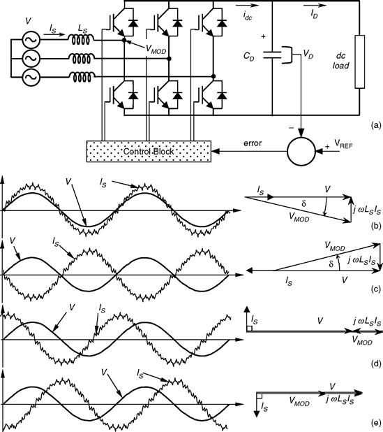
FIGURE 12.39 Four-quadrant operation of the force-commutated rectifier: (a) the PWM force-commutated rectifier; (b) rectifier operation at unity power factor; (c) inverter operation at unity power factor; (d) capacitor operation at zero power factor; and (e) inductor operation at zero power factor.
In Fig. 12.39, Is is the rms value of the source current is. This current flows through the semiconductors in the way shown in Fig. 12.40. During the positive half cycle, the transistor TN, connected at the negative side of the dc link is switched ON, and the current is begins to flow through TN (iTn) The current returns to the mains and comes back to the valves, closing a loop with another phase, and passing through a diode connected at the same negative terminal of the dc link. The current can also go to the dc load (inversion) and return through another transistor located at the positive terminal of the dc link. When the transistor TN is switched OFF, the current path is interrupted and the current begins to flow through the diode Dp, connected at the positive terminal of the dc link. This current, called iDp in Fig. 12.39, goes directly to the dc link, helping in the generation of the current idc. The current idc charges the capacitor CD and permits the rectifier to produce dc power. The inductances Ls are very important in this process, because they generate an induced voltage which allows the conduction of the diode Dp. Similar operation occurs during the negative half cycle, but with Tp and DN (see Fig. 12.40).

FIGURE 12.40 Current waveforms through the mains, the valves, and the dc link.
Under inverter operation, the current paths are different because the currents flowing through the transistors come mainly from the dc capacitor, CD Under rectifier operation, the circuit works like a boost converter and under inverter, it works as a buck converter.
To have full control of the operation of the rectifier, their six diodes must be polarized negatively at all values of instantaneous ac voltage supply. Otherwise diodes will conduct, and the PWM rectifier will behave like a common diode rectifier bridge. The way to keep the diodes blocked is to ensure a dc link voltage higher than the peak dc voltage generated by the diodes alone, as shown in Fig. 12.41. In this way, the diodes remain polarized negatively, and they will conduct only when at least one transistor is switched ON, and favorable instantaneous ac voltage conditions are given. In the Fig. 12.41, VD represents the capacitor dc voltage, which is kept higher than the normal diode-bridge rectification value vBRIDGE. To maintain this condition, the rectifier must have a control loop like the one displayed in Fig. 12.36.
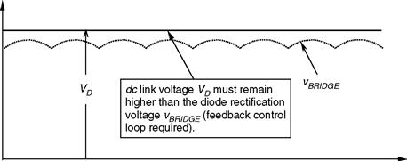
FIGURE 12.41 The DC link voltage condition for the operation of the PWM rectifier.
12.3.3 PWM Phase-to-phase and Phase-to-neutral Voltages
The PWM waveforms shown in the preceding figures are voltages measured between the middle point of the dc voltage and the corresponding phase. The phase-to-phase PWM voltages can be obtained with the help of Eq. (12.52), where the voltageVABPWM is evaluated.
![]() (12.52)
(12.52)
where VAPWM and VBPWM are the voltages measured between the middle point of the dc voltage, and the phases a and b respectively. In a less straightforward fashion, the phase-to-neutral voltage can be evaluated with the help of Eq. (12.53).
![]() (12.53)
(12.53)
where VANPWM is the phase-to-neutral voltage for phase a, and VjkPWM is the phase-to-phase voltage between phase j and phase k. Figure 12.42 shows the PWM patterns for the phase-to-phase and phase-to-neutral voltages.

FIGURE 12.42 PWM phase voltages: (a) PWM phase modulation; (b) PWM phase-to-phase voltage; and (c) PWM phase-to-neutral voltage.
12.3.4 Control of the DC Link Voltage
Control of the dc link voltage requires a feedback control loop. As already explained in Section 12.3.2, the dc voltage Vd is compared with a reference Vref and the error signal “e” obtained from this comparison is used to generate a template waveform. The template should be a sinusoidal waveform with the same frequency of the mains supply. This template is used to produce the PWM pattern and allows controlling the rectifier in two different ways: (1) as a voltage-source current-controlled PWM rectifier or (2) as a voltage-source voltage-controlled PWM rectifier. The first method controls the input current, and the second controls the magnitude and phase of the voltage VMOD. The current-controlled method is simpler and more stable than the voltage-controlled method, and for these reasons it will be explained first.
12.3.4.1 Voltage-source Current-controlled PWM Rectifier
This method of control is shown in the rectifier in Fig. 12.43. Control is achieved by measuring the instantaneous phase currents and forcing them to follow a sinusoidal current reference template, I_ref. The amplitude of the current reference template, IMAX is evaluated using the following equation

FIGURE 12.43 Voltage-source current-controlled PWM rectifier.
![]() (12.54)
(12.54)
where GC is shown in Fig. 12.43 and represents a controller such as PI, P, Fuzzy, or other. The sinusoidal waveform of the template is obtained by multiplying IMAX with a sine function, with the same frequency of the mains, and with the desired phase-shift angle φ, as shown in Fig. 12.43. Further, the template must be synchronized with the power supply. After that, the template has been created and is ready to produce the PWM pattern.
However, one problem arises with the rectifier because the feedback control loop on the voltage VC can produce instability. Then it becomes necessary to analyze this problem during rectifier design. Upon introducing the voltage feedback and the GC controller, the control of the rectifier can be represented in a block diagram in Laplace dominion, as shown in Fig. 12.44. This block diagram represents a linearization of the system around an operating point, given by the rms value of the input current, Is.

FIGURE 12.44 Closed-loop rectifier transfer function.
The blocks G1(s) and G2(s) in Fig. 12.44 represent the transfer function of the rectifier (around the operating point) and the transfer function of the dc link capacitor CD respectively.
![]() (12.55)
(12.55)
where ΔP1(s) and ΔP2(s) represent the input and output power of the rectifier in Laplace dominion, V the rms value of the mains voltage supply (phase-to-neutral), Is the input current being controlled by the template, Ls the input inductance, and R the resistance between the converter and power supply. According to stability criteria, and assuming a PI controller, the following relations are obtained
![]() (12.57)
(12.57)
These two relations are useful for the design of the current-controlled rectifier. They relate the values of dc link capacitor, dc link voltage, rms voltage supply, input resistance and inductance, and input power factor, with the rms value of the input current, Is. With these relations the proportional and integral gains Kp and KI can be calculated to ensure the stability of the rectifier. These relations only establish limitations for rectifier operation, because negative currents always satisfy the inequalities.
With these two stability limits satisfied, the rectifier will keep the dc capacitor voltage at the value of VREF (PI controller), for all load conditions, by moving power from the ac to the dc side. Under inverter operation, the power will move in the opposite direction.
Once the stability problems have been solved and the sinusoidal current template has been generated, a modulation method will be required to produce the PWM pattern for the power valves. The PWM pattern will switch the power valves to force the input currents I_line to follow the desired current template I_ref. There are many modulation methods in the literature, but three methods for voltage-source current-controlled rectifiers are the most widely used ones: periodical sampling (PS), hysteresis band (HB), and triangular carrier (TC).
The PS method switches the power transistors of the rectifier during the transitions of a square wave clock of fixed frequency: the periodical sampling frequency. In each transition, a comparison between I_ref and I_line is made, and corrections take place. As shown in Fig. 12.45a, this type of control is very simple to implement: only a comparator and a D-type flip-flop are needed per phase. The main advantage of this method is that the minimum time between switching transitions is limited to the period of the sampling clock. This characteristic determines the maximum switching frequency of the converter. However, the average switching frequency is not clearly defined.

FIGURE 12.45 Modulation control methods: (a) periodical sampling; (b) hysteresis band; and (c) triangular carrier.
The HB method switches the transistors when the error between I_ref and I_line exceeds a fixed magnitude: the hysteresis band. As it can be seen in Fig. 12.45b, this type of control needs a single comparator with hysteresis per phase. In this case the switching frequency is not determined, but its maximum value can be evaluated through the following equation
![]() (12.59)
(12.59)
where h is the magnitude of the hysteresis band.
The TC method, shown in Fig. 12.45c, compares the error between I_ref and I_line with a triangular wave. This triangular wave has fixed amplitude and frequency and is called the triangular carrier. The error is processed through a proportional-integral (PI) gain stage before comparison with the TC takes place. As can be seen, this control scheme is more complex than PS and HB. The values for kp and ki determine the transient response and steady-state error of the TC method. It has been found empirically that the values for kp and ki shown in Eqs. (12.60) and (12.61) give a good dynamic performance under several operating conditions.
![]() (12.60)
(12.60)
where Ls is the total series inductance seen by the rectifier, ωc is the TC frequency, and VD is the dc link voltage of the rectifier.
In order to measure the level of distortion (or undesired harmonic generation) introduced by these three control methods, Eq. (12.62) is defined
 (12.62)
In Eq. (12.62), the term Irms is the effective value of the desired current. The term inside the square root gives the rms value of the error current, which is undesired. This formula measures the percentage of error (or distortion) of the generated waveform. This definition considers the ripple, amplitude, and phase errors of the measured waveform, as opposed to the THD, which does not take into account off sets, scalings, and phase shifts.
Figure 12.46 shows the current waveforms generated by the three aforementioned methods. The example uses an average switching frequency of 1.5 kHz. The PS is the worst, but its digital implementation is simpler. The HB method and TC with PI control are quite similar, and the TC with only proportional control gives a current with a small phase shift. However, Fig. 12.47 shows that the higher the switching frequency, the closer the results obtained with the different modulation methods. Over 6 kHz of switching frequency, the distortion is very small for all methods.

FIGURE 12.46 Waveforms obtained using 1.5 kHz switching frequency and Ls = 13 mH: (a) PS method; (b) HB method; (c) TC method (KP + KI); and (d) TC method (KP only).

FIGURE 12.47 Distortion comparison for a sinusoidal current reference.
12.3.4.2 Voltage-source Voltage-controlled PWM Rectifier
Figure 12.48 shows a one-phase diagram from which the control system for a voltage-source voltage-controlled rectifier is derived. This diagram represents an equivalent circuit of the fundamentals, that is, pure sinusoidal at the mains side and pure dc at the dc link side. The control is achieved by creating a sinusoidal voltage template VMOD which is modified in amplitude and angle to interact with the mains voltage V. In this way the input currents are controlled without measuring them. The template VMOD is generated using the differential equations that govern the rectifier.

FIGURE 12.48 One-phase fundamental diagram of the voltage source rectifier.
The following differential equation can be derived from Fig. 12.48
![]() (12.63)
(12.63)
Assuming that ![]() , then the solution for is(t), to acquire a template VMOD able to make the rectifier work at constant power factor, should be of the form
, then the solution for is(t), to acquire a template VMOD able to make the rectifier work at constant power factor, should be of the form
![]() (12.64)
(12.64)
Equations (12.63), (12.64), and v(t) allows a function of time able to modify VMOD in amplitude and phase that will make the rectifier work at a fixed power factor. Combining these equations with v(t) yields
 (12.65)
Equation (12.65) provides a template for VMOD, which is controlled through variations of the input current amplitude Imax. Substituting the derivatives of Imax into Eq. (12.65) make sense, because Imax changes every time the dc load is modified. The term Xs in Eq. (12.65) is ωLs. This equation can also be written for unity power factor operation. In such a case, cos φ = 1 and sin φ = 0.
 (12.66)
With this last equation, a unity power factor, voltage source, voltage-controlled PWM rectifier can be implemented as shown in Fig. 12.49. It can be observed that Eqs. (12.65) and (12.66) have an in-phase term with the mains supply (sin ωt) and an in-quadrature term (cos ωt). These two terms allow the template VMOD to change in magnitude and phase so as to have full unity power factor control of the rectifier.

FIGURE 12.49 Implementation of the voltage-controlled rectifier for unity power factor operation.
Compared with the control block of Fig. 12.43, in the voltage-source voltage-controlled rectifier of Fig. 12.49, there is no need to sense the input currents. However, to ensure stability limits as good as the limits of the current-controlled rectifier, the blocks “-R-sLs” and “-Xs” in Fig. 12.49, have to emulate and reproduce exactly the real values of R, Xs, and Ls of the power circuit. However, these parameters do not remain constant, and this fact affects the stability of this system, making it less stable than the system showed in Fig. 12.43. In theory, if the impedance parameters are reproduced exactly, the stability limits of this rectifier are given by the same equations as used for the current-controlled rectifier seen in Fig. 12.43 (Eqs. (12.57) and (12.58)).
Under steady-state, Imax is constant, and Eq. (12.66) can be written in terms of phasor diagram, resulting in Eq. (12.67). As shown in Fig. 12.50, different operating conditions for the unity power factor rectifier can be displayed with this equation

FIGURE 12.50 Steady-state operation of the unity power factor rectifier under different load conditions.
![]() (12.67)
(12.67)
With the sinusoidal template VMOD already created, a modulation method to commutate the transistors will be required. As in the case of current-controlled rectifier, there are many methods to modulate the template, with the most well known the so-called sinusoidal pulse width modulation (SPWM), which uses a TC to generate the PWM as shown in Fig. 12.51. Only this method will be described in this chapter.

FIGURE 12.51 Sinusoidal modulation method based on TC.
In this method, there are two important parameters to define: the amplitude modulation ratio or modulation index m, and the frequency modulation ratio p. Definitions are given by
![]() (12.68)
(12.68)
where VmaxMOD and VmaxTRIANG are the amplitudes of VMOD and VTRIANG respectively. On the other hand, fs is the frequency of the mains supply and fT the frequency of the TC. In Fig. 12.51, m = 0.8 and p = 21. When m > 1 overmodulation is defined. The modulation method described in Fig. 12.51 has a harmonic content that changes with p and m. When p < 21, it is recommended that synchronous PWM be used, which means that the TC and the template should be synchronized. Furthermore, to avoid subharmonics, it is also desired that p be an integer. If p is an odd number, even harmonics will be eliminated. If p is a multiple of 3, then the PWM modulation of the three phases will be identical. When m increases, the amplitude of the fundamental voltage increases proportionally, but some harmonics decrease. Under overmodulation (m > 1), the fundamental voltage does not increase linearly, and more harmonics appear. Figure 12.52 shows the harmonic spectrum of the three-phase PWM voltage waveforms for different values of m, and p = 3k where k is an odd number.

FIGURE 12.52 Harmonic spectrum for SPWM modulation.
Due to the presence of the input inductance Ls, the harmonic currents that result are proportionally attenuated with the harmonic number. This characteristic is shown in the current waveforms of Fig. 12.53, where larger p numbers generate cleaner currents. The rectifier that originated the currents of Fig. 12.53 has the following characteristics: VD = 450 Vdc, Vrmsf–f = 220 Vac, Ls = 2 mH, and input current Is = 80 Arms. It can be observed that with p < 21 the current distortion is quite small. The value of p = 81 in Fig. 12.53 produces an almost pure sinusoidal waveform, and it means 4860 Hz of switching frequency at 60 Hz or only 4.050 Hz in a rectifier operating in a 50 Hz supply. This switching frequency can be managed by MOSFETs, IGBTs, and even Power Darlingtons. Then a number p = 81, is feasible for today's low and medium power rectifiers.

FIGURE 12.53 Current waveforms for different values of p.
12.3.4.3 Voltage-source Load-controlled PWM Rectifier
A simple method of control for small PWM rectifiers (up to 10–20 kW) is based on direct control of the dc current. Figure 12.54 shows the schematic of this control system. The fundamental voltage VMOD modulated by the rectifier is produced by a fixed and unique PWM pattern, which can be carefully selected to eliminate most undesirable harmonics. As the PWM does not change, it can be stored in a permanent digital memory (ROM).

FIGURE 12.54 Voltage-source load-controlled PWM rectifier.
The control is based on changing the power angle δ between the mains voltage V and fundamental PWM voltage VMOD When δ changes, the amount of power flow transferred from the ac to the dc side also changes. When the power angle is negative (VMOD lags V), the power flow goes from the ac to the dc side. When the power angle is positive, the power flows in the opposite direction. Then, the power angle can be controlled through the current ID The voltage VD does not need to be sensed, because this control establishes a stable dc voltage operation for each dc current and power angle. With these characteristics, it is possible to find a relation between ID and δ so as to obtain constant dc voltage for all load conditions.
 (12.70)
From Eq. (12.70) a plot and a reciprocal function δ=f(ID) is obtained to control the rectifier. The relation between ID and δ allows for leading power factor operation and null regulation. The leading power factor operation is shown in the phasor diagram of Fig. 12.54.
The control scheme of the voltage-source load-controlled rectifier is characterized by the following: (i) there are neither input current sensors nor dc voltage sensor; (ii) it works with a fixed and predefined PWM pattern; (iii) it presents very good stability; (iv) its stability does not depend on the size of the dc capacitor; (v) it can work at leading power factor for all load conditions; and (vi) it can be adjusted with Eq. (12.70) to work at zero regulation. The drawback appears when R in Eq. (12.70) becomes negligible, because in such a case the control system is unable to find an equilibrium point for the dc link voltage. That is why this control method is not applicable to large systems.
12.3.5 New Technologies and Applications of Force-commutated Rectifiers
The additional advantages of force-commutated rectifiers with respect to line-commutated rectifiers, make them better candidates for industrial requirements. They permit new applications such as rectifiers with harmonic elimination capability (active filters), power factor compensators, machine drives with four-quadrant operation, frequency links to connect 50 Hz with 60 Hz systems, and regenerative converters for traction power supplies. Modulation with very fast valves such as IGBTs permit almost sinusoidal currents to be obtained. The dynamics of these rectifiers is so fast that they can reverse power almost instantaneously. In machine drives, current source PWM rectifiers, like the one shown in Fig. 12.35a, can be used to drive dc machines from the three-phase supply. Four-quadrant applications using voltage-source PWM rectifiers, are extended for induction machines, synchronous machines with starting control, and special machines such as brushless-dc motors. Back-to-back systems are being used in Japan to link power systems with different frequencies.
12.3.5.1 Active Power Filter
Force-commutated PWM rectifiers can work as active power filters. The voltage-source current-controlled rectifier has the capability to eliminate harmonics produced by other polluting loads. It only needs to be connected as shown in Fig. 12.55.

FIGURE 12.55 Voltage-source rectifier with harmonie elimination capability.
The current sensors are located at the input terminals of the power source and these currents (instead of the rectifier currents) are forced to be sinusoidal. As there are polluting loads in the system, the rectifier is forced to deliver the harmonics that loads need, because the current sensors do not allow the harmonics going to the mains. As a result, the rectifier currents become distorted, but an adequate dc capacitor CD can keep the dc link voltage in good shape. In this way the rectifier can do its duty, and also eliminate harmonics to the source. In addition, it also can compensate power factor and unbalanced load problems.
12.3.5.2 Frequency Link Systems
Frequency link systems permit power to be transferred form one frequency to another one. They are also useful for linking unsynchronized networks. Line-commutated converters are widely used for this application, but they have some drawbacks that force-commutated converters can eliminate. For example, the harmonic filters requirement, the poor power factor, and the necessity to count with a synchronous compensator when generating machines at the load side are absent. Figure 12.56 shows a typical line-commutated system in which a 60 Hz load is fed by a 50 Hz supply. As the 60 Hz side needs excitation to commutate the valves, a synchronous compensator has been required.

FIGURE 12.56 Frequency link systems with line-commutated converters.
In contrast, an equivalent system with force-commutated converters is simpler, cleaner, and more reliable. It is implemented with a dc voltage-controlled rectifier, and another identical converter working in the inversion mode. The power factor can be adjusted independently at the two ac terminals, and filters or synchronous compensators are not required. Figure 12.57 shows a frequency link system with force-commutated converters.

FIGURE 12.57 Frequency link systems with force-commutated converters.
12.3.5.3 Special Topologies for High Power Applications
High power applications require series- and/or parallel-connected rectifiers. Series and parallel operation with force-commutated rectifiers allow improving the power quality because harmonic cancellation can be applied to these topologies. Figure 12.58 shows a series connection of force-commutated rectifiers, where the modulating carriers of the valves in each bridge are shifted to cancel harmonics. The example uses sinusoidal PWM that are with TC shifted.

FIGURE 12.58 Series connection system with force-commutated rectifiers.
The waveforms of the input currents for the series connection system are shown in Fig. 12.59. The frequency modulation ratio shown in this figure is for p = 9. The carriers are shifted by 90° each, to obtain harmonics cancellation. Shifting of the carriers δT depends on the number of converters in series (or in parallel), and is given by

FIGURE 12.59 Input currents and carriers of the series connection system of Fig. 12.58.
![]() (12.71)
(12.71)
where n is the number of converters in series or in parallel. It can be observed that despite the low value of p, the total current becomes quite clean and clear, better than the current of one of the converters in the chain.
The harmonic cancellation with series- or parallel-connected rectifiers, using the same modulation but the carriers shifted, is quite effective. The resultant current is better with n converters and frequency modulation p = p1 than with one converter and p = n · p1. This attribute is verified in Fig. 12.60, where the total current of four converters in series with p = 9 and carriers shifted, is compared with the current of only one converter and p = 36. This technique also allows for the use of valves with slow commutation times, such as high power GTOs. Generally, high power valves have low commutation times and hence the parallel and/or series options remain very attractive.

FIGURE 12.60 Four converters in series and p = 9 compared with one converter and p = 36.
Another special topology for high power was implemented for Asea Brown Boveri (ABB) in Bremen. A 100 MW power converter supplies energy to the railways at 162/3 Hz. It uses basic “H” bridges like the one shown in Fig. 12.61, connected to the load through power transformers. These transformers are connected in parallel at the converter side, and in series at the load side.

FIGURE 12.61 The “H” modulator: (a) one bridge and (b) bridges connected in series at load side through isolation transformers.
The system uses SPWM with TCs shifted, and depending on the number of converters connected in the chain of bridges, the voltage waveform becomes more and more sinusoidal. Figure 12.62 shows a back-to-back system using a chain of 12 “H” converters connected as showed in Fig. 12.61b.

FIGURE 12.62 Frequency link with force-commutated converters and sinusoidal voltage modulation.
The ac voltage waveform obtained with the topology of Fig. 12.62 is displayed in Fig. 12.63. It can be observed that the voltage is formed by small steps that depend on the number of converters in the chain (12 in this case). The current is almost perfectly sinusoidal.

FIGURE 12.63 Voltage and current waveforms with 12 converters.
Figure 12.64 shows the voltage waveforms for different number of converters connected in the bridge. It is clear that the larger the number of converters, the better the voltage.

FIGURE 12.64 Voltage waveforms with different numbers of “H” bridges in series.
Another interesting result with this converter is that the ac voltages become modulated by both PWM and amplitude modulation (AM). This is because when the pulse modulation changes, the steps of the amplitude change. The maximum number of steps of the resultant voltage is equal to the number of converters. When the voltage decreases, some steps disappear, and then the AM becomes a discrete function. Figure 12.65 shows the AM of the voltage.

FIGURE 12.65 Amplitude modulation of the “H” bridges of Fig. 12.62.
12.3.5.4 Machine Drives Applications
One of the most important applications of force-commutated rectifiers is in machine drives. Line-commutated thyristor converters have limited applications because they need excitation to extinguish the valves. This limitation do not allow the use of line-commutated converters in induction machine drives.
On the other hand, with force-commutated converters four-quadrant operation is achievable. Figure 12.66 shows a typical frequency converter with a force-commutated rectifier–inverter link. The rectifier side controls the dc link, and the inverter side controls the machine. The machine can be a synchronous, brushless dc, or induction machine. The reversal of both speed and power are possible with this topology. At the rectifier side, the power factor can be controlled, and even with an inductive load such as an induction machine, the source can “see” the load as capacitive or resistive. Changing the frequency of the inverter controls the machine speed, and the torque is controlled through the stator currents and torque angle. The inverter will become a rectifier during regenerative braking, which is possible by making slip negative in an induction machine, or by making the torque angle negative in synchronous and brushless dc machines.

FIGURE 12.66 Frequency converter with force-commutated converters.
A variation of the drive of Fig. 12.66 is found in electric traction applications. Battery powered vehicles use the inverter as a rectifier during regenerative braking, and sometimes the inverter is also used as a battery charger. In this case, the rectifier can be fed by a single-phase or three-phase system. Figure 12.67 shows a battery-powered electric bus system. This system uses the power inverter of the traction motor as rectifier for two purposes: regenerative braking and as a battery charger fed by a three-phase power source.

FIGURE 12.67 Electric bus system with regenerative braking and battery charger.
12.3.5.5 Variable Speed Power Generation
Power generation at 50 or 60 Hz requires constant speed machines. In addition, induction machines are not currently used in power plants because of magnetization problems. With the use of frequency-link force-commutated converters, variable-speed constant-frequency generation becomes possible even with induction generators. The power plant in Fig. 12.68 shows a wind generator implemented with an induction machine, and a rectifier-inverter frequency link connected to the utility. The dc link voltage is kept constant with the converter located at the mains side. The converter connected at the machine side controls the slip of the generator and adjusts it according to the speed of wind or power requirements. The utility is not affected by the power factor of the generator, because the two converters keep the cosçϕ of the machine independent of the mains supply. The converter at the mains side can even be adjusted to operate at leading power factor.

FIGURE 12.68 Variable-speed constant-frequency wind generator.
Varible-speed constant-frequency generation also can be used in either hydraulic or thermal plants. This allows for optimal adjustment of the efficiency-speed characteristics of the machines. In many places, wound rotor induction generators working as variable speed synchronous machines are being used as constant frequency generators. They operate in hydraulic plants that are able to store water during low demand periods. A power converter is connected at the slip rings of the generator. The rotor is then fed with variable frequency excitation. This allows the generator to generate at different speeds around the synchronous rotating flux.
12.3.5.6 Power Rectifiers Using Multilevel Topologies
Almost all voltage source rectifiers already described are two-level configurations. Today, multilevel topologies are becoming very popular, mainly three-level converters. The most popular three-level configuration is called diode clamped converter, which is shown in Fig. 12.69. This topology is today the standard solution for high power steel rolling mills, which uses back-to-back three-phase rectifier–inverter link configuration. In addition, this solution has been recently introduced in high power downhill conveyor belts which operate almost permanently in the regeneration mode or rectifier operation. The more important advantage of three-level rectifiers is that voltage and current harmonics are reduced due to the increased number of levels.

FIGURE 12.69 Voltage-source rectifier using three-level converter.
Higher number of levels can be obtained using the same diode clamped strategy, as shown in Fig. 12.70, where only one phase of a general approach is displayed. However, this topology becomes more and more complex with the increase of number of levels. For this reason, new topologies are being studied to get a large number of levels with less power transistors. One example of such of these topologies is the multistage, 27-level converter shown in Fig. 12.71. This special 27-level, four-quadrant rectifier, uses only three H-bridges per phase with independent input transformers for each H-bridge. The transformers allow galvanic isolation and power escalation to get high quality voltage waveforms, with THD of less than 1%. The power scalation consists on increasing the voltage rates of each transformer making use of the “three-level” characteristics of H-bridges. Then, the number of levels is optimized when transformers are scaled in power of three. Some advantages of this 27-level topology are: (a) only one of the three H-bridges, called “main converter,” manages more than 80% of the total active power in each phase and (b) this main converter switches at fundamental frequency reducing the switching losses at a minimum value. The rectifier of Fig. 12.71 is a current-controlled voltage source type, with a conventional feedback control loop, which is being used as a rectifier in a subway substation. It includes fast reversal of power and the ability to produce clean ac and dc waveforms with negligible ripple. This rectifier can also compensate power factor and eliminate harmonics produced by other loads in the ac line. Figure 12.72 shows the ac voltage waveform obtained with this rectifier from an experimental prototype. If one more H-bridge is added, 81 levels are obtained, because the number of levels increases according with N = 3k, where N is the number of levels or voltage steps and k the number of H-bridges used per phase.

FIGURE 12.70 Multilevel rectifier using diode clamped topology.

FIGURE 12.71 27-Level rectifier for railways, using H-bridges scaled in power of three.
FIGURE 12.72 AC voltage waveform generated by the 27-level rectifier.
Many other high-level topologies are under study but this matter is beyond the main topic of this chapter.
Further Reading
1. MÖltgen G. Line Commutated Thyristor Converters. Siemens Aktiengesellschaft, Berlin-Munich. London: Pitman Publishing; 1972.
2. MÖltgen G. Converter Engineering, and Introduction to Operation and Theory. New York: John Wiley and Sons; 1984.
3. Thorborg K. Power Electronics. London: Prentice-Hall International (UK) Ltd.; 1988.
4. Rashid MH. Power Electronics, Circuits Devices and Applications. London: Prentice-Hall International Editions; 1992.
5. Mohan N, Undeland TM, Robbins WP. Power Electronics: Converters, Applications, and Design. New York: John Wiley and Sons; 1989.
6. Arrillaga J, Bradley DA, Bodger PS. Power System Harmonics. New York: John Wiley and Sons; 1989.
7. Murphy JMD, Turnbull FG. Power Electronic Control of AC Motors. Pergamon Press 1988.
8. Villablanca ME, Arrillaga J. Pulse Multiplication in Parallel Convertors by Multitap Control of Interphase Reactor. IEE Proceedings-B. January 1992; vol. 139 [pp. 13–20].
9. Woodford DA. HVDC Transmission. Professional Report from Manitoba HVDC Research Center, Winnipeg, Manitoba. March 1998.
10. Veas DR, Dixon JW, Ooi BT. A Novel Load Current Control Method for a Leading Power Factor Voltage Source PEM Rectifier. IEEE Transactions on Power Electronics. March 1994; vol. 9(No 2):153–159.
11. Morán L, Mora E, Wallace R, Dixon J. Performance Analysis of a Power Factor Compensator which Simultaneously Eliminates Line Current Harmonics. IEEE Power Electronics Specialists Conference. 1992.
12. Ziogas PD, Morán L, Joos G, Vincenti D. A Refined PWM Scheme for Voltage and Current Source Converters. IEEE-IAS Annual Meeting. 1990; 977–983.
13. McMurray W. Modulation of the Chopping Frequency in DC Choppers and PWM Inverters Having Current Hysteresis Controllers. IEEE Transaction on Ind. Appl.. July/August 1984; vol. IA-20:763–768.
14. Dixon JW, Ooi BT. Indirect Current Control of a Unity Power Factor Sinusoidal Current Boost Type Three-Phase Rectifier. IEEE Transactions on Industrial Electronics. November 1988; vol. 35(No 4):508–515.
15. Morán L, Dixon J, Wallace R. A Three-Phase Active Power Filter Operating with Fixed Switching Frequency for Reactive Power and Current Harmonic Compensation. IEEE Transactions on Industrial Electronics. August 1995; vol. 42(No 4):402–408.
16. Boost MA, Ziogas P. State-of-the-Art PWM Techniques, a Critical Evaluation. IEEE Transactions on Industry Applications. March/April 1988; vol. 24(No 2):271–280.
17. Dixon JW, Ooi BT. Series and Parallel Operation of Hysteresis Current-Controlled PWM Rectifiers. IEEE Transactions on Industry Applications. July/August 1989; vol. 25(No 4):644–651.
18. Ooi BT, Dixon JW, Kulkarni AB, Nishimoto M. An integrated AC Drive System Using a Controlled-Current PWM Rectifier/Inverter Link. IEEE Transactions on Power Electronics. January 1988; vol. 3(No 1):64–71.
19. Koyama M, Shimomura Y, Yamaguchi H, Mukunoki M, Okayama H, Mizoguchi S. Large Capacity High Efficiency Three-Level GCT Inverter System for Steel Rolling Mill Drivers. Proceedings of the 9th European Conference on Power Electronics, EPE. 2001; [Austria, CDROM].
20. Rodríguez J, Dixon J, Espinoza J, Lezana P. PWM Regenerative Rectifiers: State of the Art. IEEE Transactions on Industrial Electronics. January/February 2005; vol. 52(No 4):5–22.
21. Dixon J, Morán L. A Clean Four-Quadrant Sinusoidal Power Rectifier, Using Multistage Converters for Subway Applications. IEEE Transactions on Industrial Electronics. May–June 2005; vol. 52(No 5):653–661.