
19
Power Factor Correction Circuits
School of Electrical Engineering and Computer Science, University of Central Florida, 4000 Central Florida Blvd., Orlando, Florida, USA
19.1 Introduction
19.3.1 Energy Balance in PFC Circuits
19.3.2 Passive Power Factor Corrector
19.3.3 Basic Circuit Topologies of Active Power Factor Correctors
19.4.1 Current Mode Control
19.4.2 Voltage Mode Control
19.5 DCM Input Technique
19.5.1 Power Factor Correction Capabilities of the Basic Converter Topologies in DCM
19.5.2 AC–DC Power Supply with DCM Input Technique
19.5.3 Other PFC Techniques
19.6 Summary
19.1 Introduction
Today, our society has become very aware of the necessity of the natural environment protection of our living plant in the face of a programmed utilization of natural resource. Like the earth, the utility power supply that we are now using was clean when it was invented in nineteenth century. Over hundred years, electrical power system has benefited people in every aspect. Meanwhile, due to the intensive use of this utility, the power supply condition becomes “polluted.” However, public concern about the “dirty” environment in the power system has not been drawn until the mid 1980s [1–6].
Since ac electrical energy is the most convenient form of energy to be generated, transmitted, and distributed, ac power systems had been swiftly introduced into industries and residences since the turn of the twentieth century. With the proliferation of utilization of electrical energy, more and more heavy loads have been connected into the power system. During 1960s, large electricity consumers such as electrochemical and electrometallurgical industries applied capacitors as VAR compensator to their systems to minimize the demanded charges from utility companies and to stabilize the supply voltages. As these capacitors present low impedance in the system, harmonic currents are drawn from the line. Owing to the non-zero system impedance, line voltage distortion will be incurred and propagated. The contaminative harmonics can decline power quality and affect the system performance in several ways:
(a) The line rms current harmonics do not deliver any real power in Watts to the load, resulting in inefficient use of equipment capacity (i.e. low power factor).
(b) Harmonics will increase conductor loss and iron loss in transformers, decreasing transmission efficiency and causing thermal problems.
(c) The odd harmonics are extremely harmful to a three-phase system, causing overload of the unprotected neutral conductor.
(d) Oscillation in power system should be absolutely prevented in order to avoid endangering the stability of system operation.
(e) High peak harmonic currents may cause automatic relay protection devices to mistrigger.
(f) Harmonics could cause other problems such as electromagnetic interference to interrupt communication, degrading reliability of electrical equipment, increasing product defective ratio, insulation failure, audible noise, etc.
Perhaps the greatest impact of harmonic pollution appeared in early 1970s when static VAR compensators (SVCs) were extensively used for electric arc furnaces, metal rolling mills, and other high power appliances. The harmonic currents produced by partial conduction of SVC are odd order, which are especially harmful to three-phase power system. Harmonics can affect operations of other devices that are connected to the same system and, in some situation, the operations of themselves that generate the harmonics.
The ever deteriorated supply environment did not become a major concern until the early 1980s when the first technical standard IEEE519-1981 with respect to harmonic control at point of common coupling (PCC) was issued [7]. The significance of issuing this standard was not only that it provided the technical reference for design engineers and manufactures, but also that it opened the door of research area of harmonic reduction and power factor correction (PFC). Stimulated by the harmonic control regulation, researchers and industry users started to develop low-cost devices and power electronic systems to reduce harmonics since it is neither economical nor necessary to eliminate the harmonics.
Research on harmonic reduction and PFC has become intensified in the early nineties. With the rapid development in power semiconductor devices, power electronic systems have matured and expanded to new and wide application range from residential, commercial, aerospace to military and others. Power electronic interfaces, such as switch mode power supplies (SMPS), are now clearly superior over the traditional linear power supplies, resulting in more and more interfaces switched into power systems. While the SMPSs are highly efficient, but because of their non-linear behavior, they draw distorted current from the line, resulting in high total harmonic distortion (THD) and low power factor (PF). To achieve a smaller output voltage ripple, practical SMPSs use a large electrolytic capacitor in the output side of the single-phase rectifier. Since the rectifier diodes conduct only when the line voltage is higher than the capacitor voltage, the power supply draws high rms pulsating line current. As a result, high THD and poor PF (usually less than 0.67) are present in such power systems [6–10]. Even though each device, individually, does not present much serious problem with the harmonic current, utility power supply condition could be deteriorated by the massive use of such systems. In recent years, declining power quality has become an important issue and continues to be recognized by government regulatory agencies. With the introduction of compulsory and more stringent technical standard such as IEC1000-3-2, more and more researchers from both industries and universities are focusing in the area of harmonic reduction and PFC, resulting in numerous circuit topologies and control strategies. Generally, the solution for harmonic reduction and PFC are classified into passive approach and active approach. The passive approach offers the advantages of high reliability, high power handling capability, and easy to design and maintain. However, the operation of passive compensation system is strongly dependent on the power system and does not achieve high PF. While the passive approach can be still the best choice in many high power applications, the active approach dominates the low to medium power applications due to their extraordinary performance (PF and efficiency approach to 100%), regulation capabilities, and high density. With the power handling capability of power semiconductor devices being extended to megawatts, the active power electronic systems tend to replace most of the passive power processing devices [2–4].
Today’s harmonic reduction and PFC techniques to improve distortion are still under development. Power supply industries are undergoing the change of adopting more and more PFC techniques in all off-line power supplies. This chapter presents an overview of various active harmonic reduction and PFC techniques in the open literature. The primary objective of writing this chapter is to give a brief introduction of these techniques and provide references for future researchers in this area. The discussion here includes definition of THD and PF, commonly used control strategies, and various types of converter topologies. Finally, the possible future research trends are stressed in the Summary Section.
19.2 Definition of PF and THD
Power factor is a very important parameter in power electronics because it gives a measure of how effective the real power utilization in the system is. It also represents a measure of distortion of the line voltage and the line current and phase shift between them. Referring to Fig. 19.1a, we define the input power factor (PF) at terminal a-a′ as the ratio of the average power and the apparent power measured at terminals a-a′ as described in Eq. (19.1) [7, 9, 10]
![]() (19.1)
(19.1)
where, the apparent power is defined as the product of rms values of vs(t) and is(t).
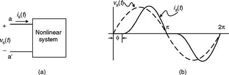
FIGURE 19.1 Non-linear load draws distorted line current.
In a linear system, because load draws purely sinusoidal current and voltage, the PF is only determined by the phase difference between vs(t) and is(t). Equation (19.1) becomes
![]() (19.2)
(19.2)
where, Is,rms and Vs,rms are rms values of line current and line voltage, respectively, and θ is the phase shift between line current and line voltage. Hence, in linear power systems, the PF is simply equal to the cosine of the phase angle between the current and voltage. However, in power electronic system, due to the non-linear behavior of active switching power devices, the phase-angle representation alone is not valid. Figure 19.1b shows that the non-linear load draws typical distorted line current from the line. Calculating PF for distorted waveforms is more complex when compared with the sinusoidal case. If both line voltage and line current are distorted, then Eqs. (19.3) and (19.4) give the Fourier expansion representations for the line current and line voltage, respectively
 (19.3)
 (19.4)
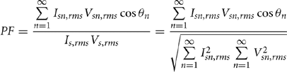
Applying the definition of PF given in Eq. (19.1) to the distorted current and voltage waveforms of Eqs. (19.3) and (19.4), PF may be expressed as
 (19.5)
where, Vsn, rms and Isn, rms are the rms values of the nth harmonic voltage and current, respectively, and θn is the phase shift between the nth harmonic voltage and current.
Since most of power electronic systems draw their input voltage from a stable line voltage source vs(t), the above expression can be significantly simplified by assuming the line voltage is pure sinusoidal and distortion is only limited to is(t), i.e.
![]() (19.6)
(19.6)
![]() (19.7)
(19.7)
Then it can be shown that the PF can be expressed as
![]() (19.8)
(19.8)
where,
θ1: the phase angle between the voltage vs(t) and the fundamental component of is(t);
Is1,rms: rms value of the fundamental component in line current;
Is,rms: total rms value of line current;
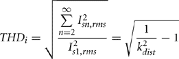
Another important parameter that measure the percentage of distortion is known as the current total harmonic distortion (THDi) which is defined as follows
 (19.9)
Conventionally SMPSs use capacitive rectifiers in front of the ac line which resulting in the capacitor voltage vc and high rms pulsating line current il(t) as shown in Fig. 19.2, when vl(t) is the line voltage. As a result, THDi is as high as 70% and poor PF is usually less than 0.67.
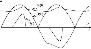
FIGURE 19.2 Typical waveforms in a poor PF system.
As we can see from Eqs. (19.8) and (19.9), PF and THD are related to distortion and displacement factors. Therefore, improvement in PF, i.e. power factor correction (PFC), also implies harmonic reduction.
19.3 Power Factor Correction
19.3.1 Energy Balance in PFC Circuits
Figure 19.3 shows a diagram of an ac–dc PFC unit. Let vl(t) and il(t) be the line voltage and line current, respectively. For an ideal PFC unit (PF = 1), we assume
(19.10a) ![]()
(19.10b) ![]()
where, Vlm and Ilm are amplitudes of line voltage and line current, respectively, and ωl is the angular line frequency. The instantaneous input power is given by
![]() (19.11)
(19.11)
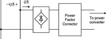
FIGURE 19.3 Block diagram of ac–dc PFC unit.
where, Pin = 1/2 Vlm Ilm is the average input power.
As we can see from Eq. (19.11), the instantaneous input power contains not only the real power (average power) Pin component but also an alternative component with frequency 2ωl (i.e. 100 or 120 Hz), shown in Fig. 19.4. Therefore, the operation principle of a PFC circuit is to process the input power in a certain way that it stores the excessive input energy (area I in Fig. 19.4) when pin(t) is larger than Pin(=Po), and releases the stored energy when pin(t) is less than Pin(=Po) to compensate for area II.
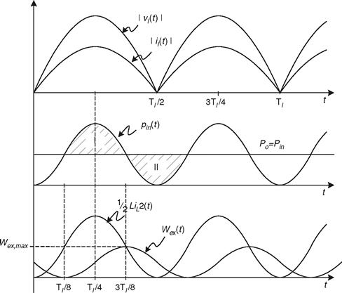
FIGURE 19.4 Energy balance in PF corrector.
The instantaneous excessive input energy, w(t), is given by
![]() (19.12)
(19.12)
At t = 3Tl/8, the excessive input energy reaches the peak value
![]() (19.13)
(19.13)
The excessive input energy has to be stored in the dynamic components (inductor and capacitor) in the PFC circuit.
In most of the PFC circuits, an input inductor is used to carry the line current. For unity PF, the inductor current (or averaged inductor current in switch mode PFC circuit) must be a pure sinusoidal and in phase with the line voltage. The energy stored in the inductor (1/2Li2L(t)) cannot completely match the change of the excessive energy as shown in Fig. 19.4. Therefore, to maintain the output power constant, another energy storage component (usually the output capacitor) is needed.
19.3.2 Passive Power Factor Corrector
Because of their high reliability and high power handling capability, passive power factor correctors are normally used in high power line applications. Series tuned LC harmonic filter is commonly used for heavy plant loads such as arc furnaces, metal rolling mills, electrical locomotives, etc. Figure 19.5 shows a connection diagram of harmonic filter together with line frequency switched reactor static VAR compensator. By tuning the filter branches to odd harmonic frequencies, the filter shunts the harmonic currents. Since each branch presents capacitive at line frequency, the filter also provides capacitive VAR for the system. The thyristor-controlled reactor keeps an optimized VAR compensation for the system so that higher PF can be maintained.
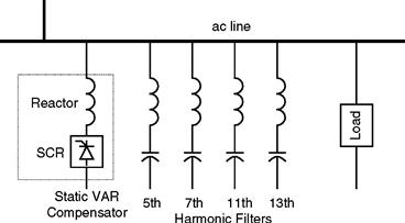
FIGURE 19.5 Series tuned LC harmonic filter PF corrector.
The design of the tuned filter PF corrector is particularly difficult because of the uncertainty of the system impedance and harmonic sources. Besides, this method involves too many expensive components and takes huge space.
For the applications where power level is less than 10 kW, the tuned filter PF corrector may not be a better choice. The most common off-line passive PF corrector is the inductive-input filter, shown in Fig. 19.6. Depending on the filter inductance, this circuit can give a maximum of 90% PF. For operation in continuous conduction mode (CCM), the PF is defined as [11]
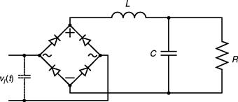
FIGURE 19.6 Inductive-input PF corrector.
![]() (19.14)
(19.14)
where
![]() (19.15)
(19.15)
The PF corrector is simply a low pass inductive filter as shown in Fig. 19.7, whose transfer function and input impedance are given by
![]() (19.16)
(19.16)
![]() (19.17)
(19.17)
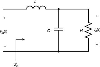
FIGURE 19.7 Low pass inductive filter.
The above equations show that the unavoidable phase displacement is incurred in the inductive-filter corrector. Because the filter frequency of operation is low (line frequency), large value inductor and capacitor have to be used. As a result, the following disadvantages are presented in most passive PF correctors:
19.3.3 Basic Circuit Topologies of Active Power Factor Correctors
In recent years, using the switched-mode topologies, many circuits and control methods are developed to comply with certain standard (such as IEEE Std 519 and IEC1000-3-2). To achieve this, high-frequency switching techniques have been used to shape the input current waveform successfully. Basically, the active PF correctors employ the six basic converter topologies or their variation versions to accomplish PFC.
A. The Buck Corrector
Figure 19.8a shows the buck PF corrector. By using PWM switch modeling technique [12], the circuit topology can be modeled by the equivalent circuit shown in Fig. 19.8b. It should be pointed out that the circuit model is a large signal model, therefore analysis of PF performance based on this model is valid. It can be shown that the transfer function and input impedance are given by
![]() (19.18)
(19.18)
![]() (19.19)
(19.19)
where d is the duty ratio of the switching signal.
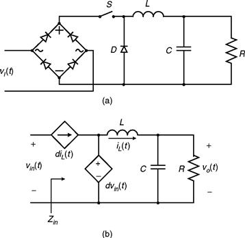
FIGURE 19.8 (a) Buck corrector and (b) PWM switch model for buck corrector.
Notice that Eqs. (19.18) and (19.19) are different from Eqs. (19.16) and (19.17), in that they have introduced the control variable d. By properly controlling the switching duty ratio to modulate the input impedance and the transfer function, a pure resistive input impedance and constant output voltage can be approached. Thereby, unity PF and output regulation can both be achieved. These control techniques will be discussed in the next section.
Comparing with the other type of high frequency PFC circuits, the buck corrector offers inrush-current limiting, overload or short-circuit protection, and over-voltage protection for the converter due to the existence of the power switch in front of the line. Another advantage is that the output voltage is lower than the peak of the line voltage, which is usually the case normally desired. The drawbacks of using buck corrector may be summarized as follows:
(a) When the output voltage is higher than the line voltage, the converter draws no current from the line, resulting in significant line current distortion near the zero-across of the line voltage;
(b) The input current is discontinuous, leading to high differential mode EMI;
B. The Boost Corrector
The boost corrector and its equivalent PWM switch modeling circuit are shown in Figs. 19.9a and b. Its transfer function and input impedance are given by
![]() (19.20)
(19.20)
![]() (19.21)
(19.21)
where d’ = 1 –d.
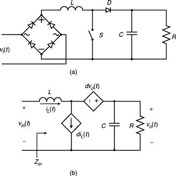
FIGURE 19.9 (a) Boost corrector and (b) PWM switch model of boost corrector.
Unlike in the buck case, it is interesting to note that in the boost case, the equivalent inductance is controlled by the switching duty ratio. Consequently, both the magnitude and the phase of the impedance, and both the dc gain and the pools of the transfer function are modulated by the duty ratio, which implies a tight control of the input current and the output voltage. Other advantages of boost corrector include less EMI and lower switch current and grounded drive. The shortcomings with the boost corrector are summarized as:
C. The Buck–Boost Corrector
The buck–boost corrector and its equivalent circuit are shown in Figs. 19.10a and b. The expressions for transfer function and input impedance are
![]() (19.22)
(19.22)
![]() (19.23)
(19.23)
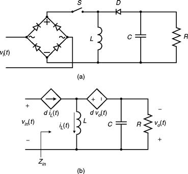
FIGURE 19.10 (a) Buck–boost corrector and (b) PWM switch model of buck–boost corrector.
The buck–boost corrector combines some advantages of the buck corrector and the boost corrector. Like a buck corrector, it can provide circuit protections and step-down output voltage, and like a boost corrector its input current waveform and output voltage can be tightly controlled. However, the buck–boost corrector has the following disadvantages:
D. The Cuk, Sepic, and Zeta Correctors
Unlike the previous converters, the Cuk, Sepic, and Zeta converters are fourth-order switching-mode circuits. Their circuit topologies for PFC are shown in Figs. 19.11a, b, and c, respectively. Because there are four energy storage components available to handle the energy balancing involved in PFC, second harmonic output voltage ripples of these correctors are smaller when compared with the second-order buck, boost, and buck–boost topologies. These PF correctors are also able to provide overload protection. However, the increased count of components and current stress are undesired.
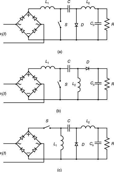
FIGURE 19.11 Fourth-order corrector: (a) Cuk corrector; (b) Sepic corrector; and (c) Zeta corrector.
19.3.4 System Configurations of PFC Power Supply
The most common configurations of ac–dc power supply with PFC are two-stage scheme and one-stage (or single-stage) scheme. In two-stage scheme as shown in Fig. 19.12a, a non-isolated PFC ac–dc converter is connected to the line to create an intermediate dc bus. This dc bus voltage is usually full of second harmonic ripple. Therefore, followed by the ac–dc converter, a dc–dc converter is cascaded to provide electrical isolation and tight voltage regulation. The advantage of two-stage structure PFC circuits is that the two power stages can be controlled separately, and thus it makes it possible to have both converters optimized. The drawbacks of this scheme are lower efficiency due to twice processing of the input power, complex control circuits, higher cost, and low reliability. Although the two-stage scheme approach is commonly adopted in industry, it received limited attention by the common research, since the input stage and output stage can be studied independently. One-stage scheme combines the PFC circuit and power conversion circuit in one stage as shown in Fig. 19.12b. Due to its simplified structure, this scheme is potentially more efficient and is very attractive in low to medium power level applications, particularly in those cost-sensitive applications. The one-stage scheme, therefore becomes the main stream of contemporary research due to the ever-increasing demands for inexpensive power supply in residential and office appliance.
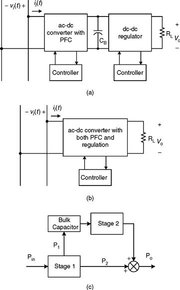
FIGURE 19.12 System configurations of PFC power supply: (a) two-stage scheme; (b) one-stage scheme; and (c) parallel scheme.
For many single-stage PFC converters, one of the most important issues is the slow dynamic response under line and load changes. To remove the low frequency ripple caused by the line (120 Hz) from the output and keep a nearly constant operation duty ratio, a large volume output capacitor is normally used. Consequently, a low frequency pole (typically less than 20 Hz) must be introduced into the feedback loop. This results in very slow dynamic response of the system [13, 14].
To avoid twice power process in two-stage scheme, two converters can be connected in parallel to form so-called parallel PFC scheme [15]. In parallel PFC circuit, power from the ac main to the load flows through two parallel paths, shown in Fig. 19.12c. The main path is a rectifier, in which power is not processed twice for PFC, whereas the other path processes the input power twice for PFC purpose. It is shown that to achieve both unity PF and tight output voltage regulation, only the difference between the input and output power within a half cycle (about 32% of the average input power) needs to be processed twice [15]. Therefore, high efficiency can be obtained by this method.
The continuous research in improving system PF has resulted in countless circuit topologies and control strategies. Classified by their principles to realize PFC, they can be mainly categorized into discontinuous conduction mode (DCM) input technique and continuous conduction mode (CCM) shaping technique. The recent research interest in DCM input technique is focused on developing PFC circuit topologies with a single power switch, result in single-stage single-switch converter (so-called S4-converter). The CCM shaping technique emphasizes on the control strategy to achieve unity input PF. The hot topics in this line of research are concentrated on degrading complexity of the control circuit and enhancing dynamic response of the system, resulting in some new control methods. Figure 19.13 shows an overview of these techniques based on conduction mode and system configuration types.
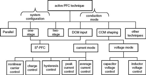
FIGURE 19.13 Overview of PFC techniques.
19.4 CCM Shaping Technique
Like other power electronic apparatus, the core of a PFC unit is its converter, which can operate either in DCM or in CCM. As shall be discussed in the next section, the benefit from DCM technique is that low-cost power supply can be achieved because of its simplified control circuit. However, the peak input current of a DCM converter is at least twice as high as its corresponding average input current, which causes higher current stresses on switches than that in a CCM converter, resulting in intolerable conduction and switching losses as well as transformer copper losses in high power applications. In practice, DCM technique is only suitable for low to medium level power application, whereas, CCM is used in high power cases. However, a converter operating in CCM does not have PFC ability inherently, i.e. unless a certain control strategy is applied, the input current will not follow the waveform of line voltage. This is why most of the research activities in improving PF under CCM condition have been focused on developing new current shaping control strategies. Depending on the system variable being controlled (either current or voltage), PFC control techniques may be classified as current control and voltage control. Current control is the most common control strategy since the primary objective of PFC is to force the input current to trace the shape of line voltage.
To achieve both PFC and output voltage regulation by using a converter operating in CCM, multiloop controls are generally used. Figure 19.14 shows the block diagram of ac–dc PFC converter with CCM shaping technique, where, Hl is a line voltage compensator, Hx is a controlled variable compensator, and x(t) is the control variable that can be either current or voltage.
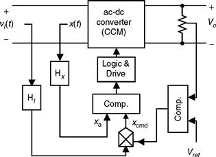
FIGURE 19.14 Block diagram of PFC converter with CCM shaping technique.
Normally, in order to obtain a sinusoidal line current and a constant dc output voltage, line voltage vl(t), output voltage Vo, and a controlled variable x(t) need to be sensed. Depending on whether the controlled variable x(t) is a current (usually the line current or the switch current) or a voltage (related to the line current), the control technique is called “current mode control” or “ voltage mode control,” respectively. In Fig. 19.14, two control loops have been applied: the feedforward loop and the feedback loops. The feedforward loop is also called “inner loop” which keeps the line current to follow the line voltage in shape and phase, while the feedback loop (also called “outer loop”) keeps the output voltage to be tightly controlled. These two loops share the same control command generated by the product of output voltage error signal and the line voltage (or rectified line voltage) signal.
19.4.1 Current Mode Control
Over many years, different current mode control techniques were developed. In this section, we will review several known methods.
A. Average Current Control
In average current control strategy, the average line current of the converter is controlled. It is more desired than the other control strategies because the line current in a SMPS can be approximated by the average current (per switching cycle) through an input EMI filter. The average current control is widely used in industries since it offers improved noise immunity, lower input ripple, and stable operation [13, 16–19].
Figure 19.15 shows a boost PFC circuit using average current control strategy. In the feedforward loop, a low value resistor Rs is used to sense the line current. Through the op-amp network formed by Ri, Rimo, Rf, Cp, Cz, and A2, average line current is detected and compared with the command current signal, icmd, which is generated by the product of line voltage signal and the output voltage error signal.
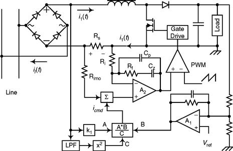
FIGURE 19.15 Boost corrector using average current control.
There is a common issue in CCM shaping technique, i.e. when the line voltage increases, the line voltage sensor provides an increased sinusoidal reference for the feedforward loop. Since the response of feedback loop is much slow than the feedforward loop, both the line voltage and the line current increase, i.e. the line current is heading to wrong changing direction (with the line voltage increasing, the line current should decrease). This results in excessive input power, causing overshoot in the output voltage. The square block, x2, in the line voltage-sensing loop shown in Fig. 19.15 provides a typical solution for this problem. It squares the output of the low-pass filter (LPF), which is in proportion to the amplitude of the line voltage, and provides the divider (A * B)/C with a squared line voltage signal for its denominator. As a result, the amplitude of the sinusoidal reference icmd is negatively proportional to the line voltage, i.e. when the line voltage changes, the control circuit leads the line current to change in the opposite direction, which is the desired situation. The detailed analysis and design issues can be found in [16–18].
As it can be seen, the average current control is a very complicated control strategy. It requires sensing the inductor current, the input voltage, and the output voltage. An amplifier for calculating the average current and a multiplier are needed. However, because of today’s advances made in IC technology, these circuits can be integrated in a single chip.
B. Variable Frequency Peak Current Control
Although the average current control is a more desired strategy, the peak current control has been widely accepted because it improves the converter efficiency and has a simpler control circuit [14, 20–24]. In variable frequency peak control strategy, shown in Fig. 19.16, the output error signal k(t) is fed back through its outer loop. This signal is multiplied by the line voltage signal αv1(t) to form a line current command signal icmd(t) (icmd(t) = αk(t) (v1 (t)). The command signal icmd(t) is the desired line current shape since it follows the shape of the line voltage. The actual line current is sensed by a transducer, resulting in signal ßi1(t) that must be reshaped to follow icmd(t) by feeding it back through the inner loop. After comparing the line current signal ßi1(t) with the command signal icmd(t), the following control strategies can be realized, depending on its logic circuit:
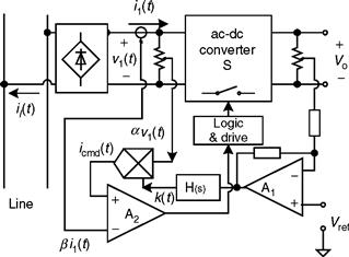
FIGURE 19.16 Block diagram for variable frequency peak current control.
Constant on-time control: Its input current waveform is given in Fig. 19.17a. Letting the fixed on-time to be Ts, the control rules are:
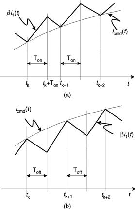
FIGURE 19.17 Input current waveforms for variable frequency peak current control: (a) constant on-time control and (b) constant off-time control.
Constant off-time control: The input current waveform is shown in Fig. 19.17b. Assuming the off-time is Toff, the control rules are:
C. Constant Frequency Peak Current Control
Generally speaking, to make it easier to design the EMI filter and to reduce harmonics, constant switching frequency ac–dc PFC converter is preferred. Based on the block diagram shown in Fig. 19.18, with Ts is the switching period, the following control rules can be considered to realize a constant frequency peak current control (shown in Fig. 19.19b):
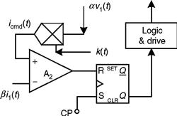
FIGURE 19.18 Logic circuit for constant frequency peak current control.
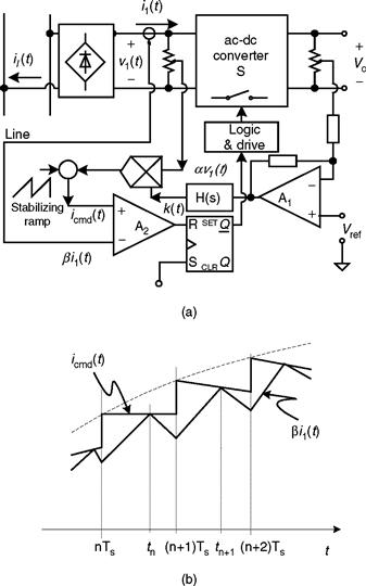
FIGURE 19.19 (a) Constant frequency peak current control with stabilizing ramp compensation and (b) line current waveform for constant frequency peak current control.
The logic circuit for the above control rules can be realized by using an R–S flip-flop with a constant frequency setting clock pulse (CP), as shown in Fig. 19.18. Unfortunately, this logic circuit will result in instability when the duty ratio exceeds 50%. This problem can be solved by subtracting a stabilizing ramp signal from the original command signal. Figure 19.19a shows a complete block diagram for typical constant frequency peak current control strategy. The line current waveform is shown in Fig. 19.19b.
It should be noticed that in both variable frequency and constant frequency peak current control strategies, either the input current or the switch current could be controlled. Thus it makes possible to apply these control methods to buck type converters. There are several advantages of using peak current control:
• The peak current can be sensed by current transformer, resulting in reduced transducer loss;
• The current-error compensator for average control method has been eliminated;
• Low gain in the feedforward loop enhances the system stability;
• The instantaneous pulse-by-pulse current limit leads to increased reliability and response speed.
However the three signals, line voltage, peak current, and output voltage signals, are still necessary to be sensed and multiplier is still needed in each of the peak current control method. Comparing with the average current control method, the input current ripple of these peak current control methods may be high when the line voltage is near the peak value. As a result, considerable line current distortion exists under high line voltage and light low operation conditions.
D. Hysteresis Control
Unlike the constant on-time and the constant off-time control, in which only one current command is used to limit either the minimum input current or the maximum input current, the hysteresis control has two current commands, ihcmd(t) and ilcmd(t) (ilcmd(t) = δihcmd(t)), to limit both the minimum and the maximum of input current [25–28]. To achieve smaller ripple in the input current, we desire a narrow hyster-band. However, the narrower the hyster-band, the higher the switching frequency. Therefore, the hyster-band should be optimized based on circuit components such as switching devices and magnetic components. Moreover, the switching frequency varies with the change of line voltage, resulting in difficulty in the design of the EMI filter. The circuit diagram and input current waveform are given in Figs. 19.20a and b, respectively. When ßi1(t) ≥ ihcmd(t), a negative pulse is generated by comparator A1 to reset the R–S flip-flop. When ßi1(t) ≤ ilcmd(t), a negative pulse is generated by comparator A2 to set the R–S flip-flop. The control rules are:
• At t = tk when βi1(tk) = ilcmd(t), S is turned on;
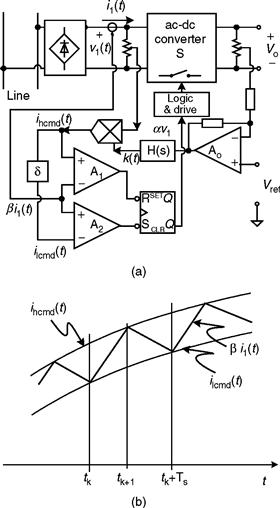
FIGURE 19.20 Hysteresis control: (a) block diagram for hysteresis control and (b) line current waveform of hysteresis control.
Like the above mentioned peak current control methods, the hysteresis control method has simpler implementation, enhanced system stability, and increased reliability and response speed. In addition, it has better control accuracy than that the peak current control methods have. However, this improvement is achieved on the penalty of wide range of variation in the switching frequency. It is also possible to improve the hysteresis control in a constant frequency operation [29, 30], but usually this will increase the complexity of the control circuit.
E. Charge Control
In order to make the average control method to be applicable for buck-derived topologies where the switch current instead of the inductor current needs to be controlled, an alternative method to realize average current control, namely, charge control was proposed in [31–33]. Since the total charge of the switch current per switching cycle is proportional to the average value of the switch current, the average current can be detected by a capacitor-switch network. Figure 19.21 shows a block diagram for charge control. The switch current is sensed by current transformer T1 and charges the capacitor CT to form average line current signal. As the switch current increases, the charge on capacitor CT also increases. When the voltage reaches the control command vc, the power switch turns off. At the same time, the switch Sd turns on to reset the capacitor. The next switching cycle begins with the power switch turning on and the switch Sd turning off by a clock pulse.
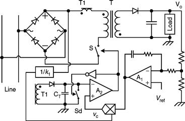
FIGURE 19.21 Flyback PFC converter using charge control.
The advantages of charge control are:
• Ability to control average switch current;
• Better switching noise immunity than peak current control;
• Elimination of turn off failure in some converters (e.g. multiresonant converter) when the switch current reaches its maximum value.
The disadvantages are:
F. Non-linear-carrier (NLC) Control
To further simplify the control circuitry, non-linear-carrier control methods were introduced [34, 35]. In CCM operation, since the input voltage is related to the output voltage through the conversion ratio, the input voltage information can be recovered by the sensed output voltage signal. Thus the sensing of input voltage can be avoided, and therefore, the multiplier is not needed, resulting in significant simplification in the control circuitry. However, complicated NLC waveform generator and its designs are involved. Figure 19.22 shows the block diagram of the NLC charge control first introduced in [34].
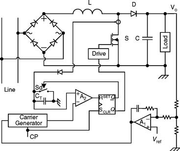
FIGURE 19.22 Boost PFC converter using NLC control.
19.4.2 Voltage Mode Control
Generally, current mode control is preferred in current source driven converters, as the boost converter. To develop controllers for voltage source driven converter, like the buck converter and to improve dynamic response, voltage mode control strategy was proposed [36, 37]. Figure 19.23 shows the input circuit of an ac–dc converter and its phasor diagram representation, where ϕ is the phase shift between the line current and the capacitor voltage. An LC network could be added to the input either before a switch mode rectifier (SMR) or after a passive rectifier to perform such kind of control. In boost type converter, the inductor Li is the input inductor. It can be seen from the phasor diagram that to keep the line current in phase with the line voltage, we can either control the capacitor voltage or the inductor voltage. If the capacitor voltage is chosen as controlled variable, the control strategy is known as delta modulation control.
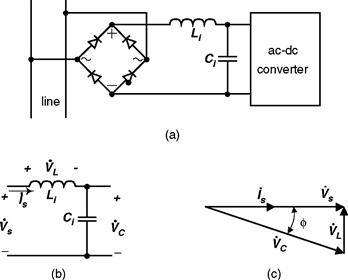
FIGURE 19.23 Input circuit and phasor diagram for voltage control: (a) input circuit of voltage control ac–dc converter; (b) simplified input circuit; and (c) phasor diagram.
A. Capacitor Voltage Control
Figure 19.24 gives a SMR with PFC using capacitor voltage control [36]. The capacitor voltage vc1(t) is forced to track a sinusoidal command v*c1(t) signal to indirectly adjust the line current in phase with the line voltage. The command signal is the product of the line voltage signal with a phase shift of ϕ and the feedback error signal. The phase shift ϕ is a function of the magnitudes of line voltage and line current, therefore the realization of a delta control is not really simple. In addition, since ϕ is usually very small, a small change in capacitor voltage will cause a large change in the inductor voltage, and hence in the line current. Thus it make the circuit very sensitive to parameter variations and perturbations.
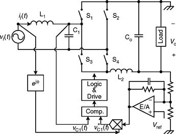
FIGURE 19.24 SMR using capacitor voltage control.
B. Inductor Voltage Control
To overcome the above shortcomings, inductor voltage control strategies was reported in [37]. Figure 19.25 shows an SMR with PFC using inductor voltage control. As the phase difference between the line voltage and the inductor voltage is fixed at 90° ideally, the control circuit is simpler in implementation than that of capacitor voltage control. As the inductor voltage is sensitive to the phase shift ϕ, but not sensitive to the change in magnitude of reference, the inductor voltage control method is more effective in keeping the line current in phase with the line voltage. However, in the implementations of both the two kinds of voltage control methods hysteresis technique is normally used. Therefore, unlike the previous current mode control, variable frequency problem is encountered in these control methods.
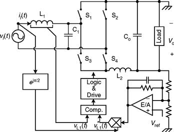
FIGURE 19.25 SMR using inductor voltage control.
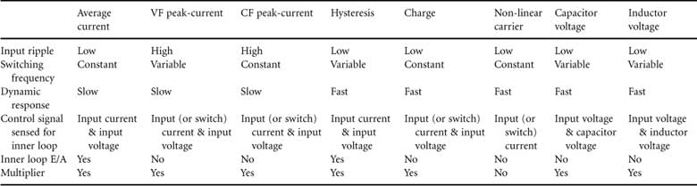
Generally speaking, by using CCM shaping technique, the input current can trace the wave shape of the line voltage well. Hence the PF can be improved efficiently. However, this technique involves in the designing of complicated control circuits. Multiloop control strategy is needed to perform input current shaping and output regulation. In most CCM shaping techniques, current sensor, and multiplier are required, which results in higher cost in practical applications. In some cases, variable frequency control is inevitable, resulting in additional difficulties in its closedloop design. Table 19.1 gives a comparison among these control methods.
TABLE 19.1 Comparison of CCM shaping techniques
19.5 DCM Input Technique
To get rid of the complicated control circuit invoked by CCM shaping technique and reduce the cost of the electronic interface, DCM input technique can be adopted in low power to medium power level application.
In DCM, the inductor current of the core converter is no longer a valid state variable since its state in a given switching cycle is independent of the value in the previous switching cycle [38]. The peak of the inductor current is sampling the line voltage automatically, resulting in sinusoidal-like average input current (line current). This is why DCM input circuit is also called “ voltage follower” or “automatic controller.” The benefit of using DCM input circuit for PFC is that no feedforward control loop is required. This is also the main advantage over a CCM PFC circuit, in which multiloop control strategy is essential. However, the input inductor operating in DCM cannot hold the excessive input energy because it must release all its stored energy before the end of each switching cycle. As a result, a bulky capacitor is used to balance the instantaneous power between the input and output. In addition, in DCM, the input current is normally a train of triangle pulses with nearly constant duty ratio. In this case, an input filter is necessary for smoothing the pulsating input current.
19.5.1 Power Factor Correction Capabilities of the Basic Converter Topologies in DCM
The DCM input circuit can be one of the basic dc–dc converter topologies. However, when they are applied to the rectified line voltage, they may draw different shapes of average line current. In order to examine the PFC capabilities of the basic converters, we first investigate their input characteristics. Because the input currents of these converters are discrete when they are operating in DCM, only averaged input currents are considered. Since switching frequency is much higher than the line frequency, let’s assume the line voltage is constant in a switching cycle. In steady state operation, the output voltage is nearly constant and the variation in duty ratio is slight. Therefore, constant duty ratio is considered in deriving the input characteristics.
A. Buck Converter
The basic buck converter topology and its input current waveform when operating in DCM are shown in Figs. 19.26a and b, respectively. It can be shown that the average input current in one switching cycle is given by
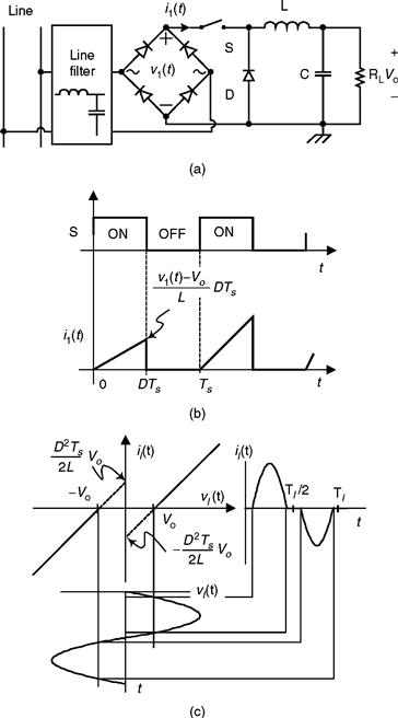
FIGURE 19.26 Input I–V characteristic of basic buck converter operating in DCM: (a) buck converter; (b) input current; and (c) input I–V characteristic.
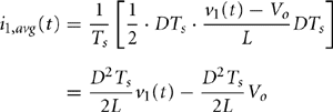 (19.24)
Figure 19.26c shows that the input voltage–input current I–V characteristic consists of two straight lines in quadrants I and III. It should be noted that these straight lines do not go through the origin. When the rectified line voltage v1(t) is less than the output voltage Vo, negative input current would occur. This is not allowed because the bridge rectifier will block the negative current. As a result, the input current is zero near the zero crossing of the line voltage, as shown in Fig. 19.26c. Actually, the input current is distorted simply because the buck converter can work only under the condition when the input voltage is larger than the output voltage. Therefore, the basic buck converter is not a good candidate for DCM input PFC.
B. Boost Converter
The basic boost converter and its input current waveform are shown in Figs. 19.27a and b, respectively. The input I–V characteristic can be found as follows
FIGURE 19.27 Input I–V characteristic of basic boost converter operating in DCM: (a) boost converter; (b) input current; and (c) input I–V characteristic.
 (19.25)
where, D1 Ts is the time during which the inductor current decreases from its peak to zero.
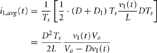
By plotting Eq. (19.25), we obtain the input I–V characteristic curve as given in Fig. 19.27c. As we can see that as long as the output voltage is larger than the peak value of the line voltage in certain range, the relationship between v1(t) and i1,avg(t) is nearly linear. When the boost converter is connected to the line, it will draw almost sinusoidal average input current from the line, shown as in Fig. 19.27c. As one might notice from Eq. (19.25) that the main reason to cause the non-linearity is the existence of D1. Ideally, if D1 = 0, the input I–V characteristic will be a linear one.
Because of the above reasons, boost converter is comparably superior to most of the other converters when applied to do PFC. However, it should be noted that boost converter can operate properly only when the output voltage is higher than its input voltage. When low voltage output is needed, a stepdown dc–dc converter must be cascaded.
C. Buck–Boost Converter
Figure 19.28a shows a basic buck–boost converter. The averaged input current of this converter can be found according to its input current waveform, shown in Fig. 19.28b.
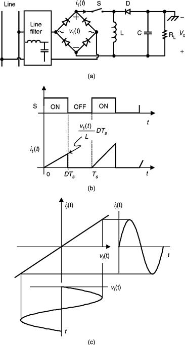
FIGURE 19.28 Input I–V characteristic of basic buck–boost converter operating in DCM: (a) buck–boost converter; (b) input current; and (c) input I–V characteristic.
![]() (19.26)
(19.26)
Equation (19.26) gives a perfect linear relationship between i1,avg(t) and v1(t), which proves that a buck–boost has an excellent automatic PFC property. This is because the input current of buck–boost converter does not related to the discharging period D1. Its input I–V characteristics and input voltage and current waveforms are shown in Fig. 19.28c. Furthermore, because the output voltage of buck–boost converter can be either larger or smaller than the input voltage, it demonstrates strong availability for DCM input technique to achieve PFC. So, theoretically buck–boost converter is a perfect candidate. Unfortunately, this topology has two limitations: (1) the polarity of its output voltage is reversed, i.e. the input voltage and the output voltage don’t have a common ground; and (2) it needs floating drive for the power switch. The first limitation circumscribes this circuit into a very narrow scope of applications. As a result, it is not widely used.
D. Flyback Converter
Flyback converter is an isolated converter whose topology and input current waveform are shown in Figs. 19.29a and b, respectively. The input voltage–input current relationship is similar to that of buck–boost converter
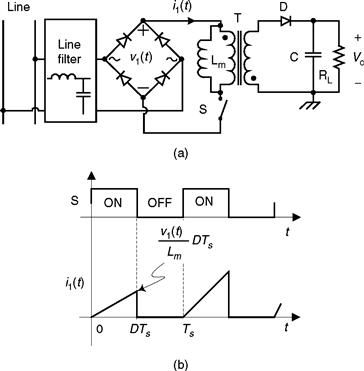
FIGURE 19.29 Input I–V characteristic of basic flyback converter operating in DCM: (a) flyback converter and (b) input current.
![]() (19.27)
(19.27)
where, Lm is the magnetizing inductance of the output transformer.
Therefore, it has the same input I–V characteristic, and hence the same input voltage and input current waveforms as those the buck–boost converter has, shown in Fig. 19.29c.
Comparing with buck–boost converter, flyback converter has all the advantages of the buck–boost converter. What’s more, input–output isolation can be provided by flyback converter. These advantages make flyback converter well suitable for PFC with DCM input technique. Comparing with boost converter, the flyback converter has better PFC and the output voltage can be either higher or lower than the input voltage. However, due to the use of power transformer, the flyback converter has high di/dt noise, lower efficiency, and lower density (larger size and heavier weight).
E. Forward Converter
The circuit shown in Fig. 19.30 is a forward converter. In order to avoid transformer saturation, it is well-known that forward converter needs the 3rd winding to demagnetize (reset) the transformer. When a forward converter is connected to the rectified line voltage, the demagnetizing current through the 3rd winding is blocked by the rectifier diodes. Therefore, forward converter is not available for PFC purpose unless a certain circuit modification is applied.
FIGURE 19.30 (a) Forward converter and (b) input current waveform.
F. Cuk Converter and Sepic Converter
It can be shown that Cuk converter and Sepic converter given in Figs. 19.31a and b, respectively, have the same input I–V characteristic. Each of these converter topologies has two inductors, with one located at its input and the other at its output. Let’s consider the case when the input inductor operates in DCM while the output inductor operates in CCM. In this case, the capacitor C1 can be designed with large value to balance the instantaneous input/output power, resulting in high PF in the input and low second harmonic ripple in the output voltage. To investigate the input characteristic of these converters, let’s take the Cuk converter as an example. One should note that the results from the Cuk converter are also suitable for Sepic converter.
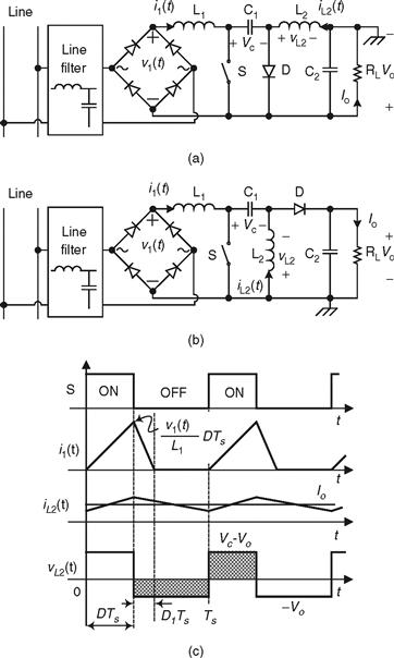
FIGURE 19.31 Input I–V characteristic of basic Cuk converter and Sepic converter operating in DCM: (a) Cuk converter; (b) Sepic converter; and (c) typical waveforms of Cuk converter with input inductor operating in DCM.
For the Cuk converter shown in Fig. 19.31a, the waveforms for input inductor current (the same as the input current), output inductor current, and the voltage across the output inductor are depicted in Fig. 19.31c. Assume that the capacitor C1 is large enough to be considered as a voltage source Vc, in steady state, employing volt-second equilibrium principle on L2, we obtain
![]() (19.28)
(19.28)
The input inductor current reset time ratio D1 is given by
![]() (19.29)
(19.29)
Therefore the averaged input current can be found as
 (19.30)
It can be seen that Eq. (19.30) is very similar to Eq. (19.25) except that the denominator in the former equation is (Vo –Dv1(t)) instead of (Vo –v1(t)). This will lead to some improvement in that I–V characteristic in Cuk converter. Referring to the I–V characteristic shown in Fig. 19.27c, Cuk converter has a curve more close to a straight line. Such improvement, however, is achieved at the expense of using more circuit components. It can be proved that the same results can be obtained by the Sepic converter.
G. Zeta Converter
Figure 19.32a gives a Zeta converter connected to the line. In DCM operation, the key waveforms are illustrated in Fig. 19.32b, where we presume the capacitor being equivalent to a voltage source Vc. As we can see that the converter input current waveform is exactly the same as that drawn by a buck–boost converter. Thus, the average input current for the Zeta converter is identical to that for the buck–boost converter, which is given by Eq. (19.26). As a result, the Zeta converter has as good automatic PFC capability as the buck–boost converter. The improvement achieved here is the non-inverted output voltage. However, like the buck converter, floating drive is required for the power switch.
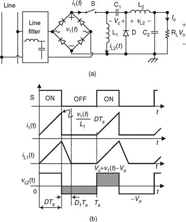
FIGURE 19.32 Input I–V characteristic of basic Zeta converter operating in DCM: (a) Zeta converter and (b) typical waveforms of Zeta converter with input inductor operating in DCM.
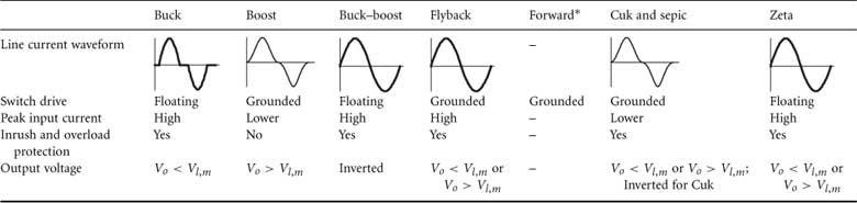
Based on the above discussion, we may conclude that all the eight basic converters except forward converter have good inherent PFC capability and are available for DCM PFC usage. Among them, boost converter and flyback converter are especially suitable for single-stage PFC scheme because they have minimum component count and grounded switch drive, and their power switches are easy to be shared with the output dc–dc converter. Hence, these two converters are most preferable by the designers for PFC purpose. The other converters could also be used to perform certain function such as circuit protection and small output voltage ripple. The characteristics of the eight basic converter topologies are summarized in Table 19.2.
TABLE 19.2 Comparison of basic converter topologies operating for DCM input technique
* The standard forward converter is not recommended as a PF corrector since the rectifier at the input will block the demagnetizing current through the tertiary winding.
19.5.2 AC–DC Power Supply with DCM Input Technique
In two-stage PFC power supply, the DCM converter is connected in front of the ac line to achieve high input PF and provide a roughly regulated dc bus voltage, as shown in Fig. 19.33. This stage is also known as “pre-regulator.” The duty ratio of the pre-regulator should be maintained relatively stable so that high PF is ensured. To stabilize the dc bus voltage, a bank capacitor is used at the output of the pre-regulator. The second stage, followed by the pre-regulator, is a dc–dc converter, called post-regulator, with its output voltage being tightly controlled. This stage can operate either in DCM or in CCM. However, CCM is normally preferred to reduce the output voltage ripple.
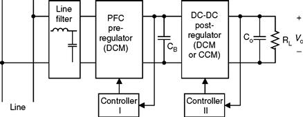
FIGURE 19.33 DCM input pre-regulator in two-stage ac–dc power supply.
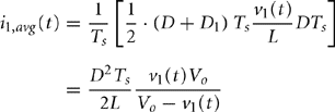
DCM input technique has been widely used in one-stage PFC circuit configurations. Using a basic converter (usually boost or flyback converter) operating in DCM, combining it with another isolation converter can form a one-stage PFC circuit. A storage capacitor is generally required to hold the dc bus voltage in these combinations. Unlike the two-stage PFC circuit, in which the bus voltage is controlled, the single-stage PFC converter has only one feedback loop from the output. The input circuit and the output circuit must share the same control signal. In [39–41] a number of combinations have been studied. Figures 19.34 and 19.35 show a few examples of successful combinations. Since the input circuit and the output circuit are in a single stage, it is possible for them to share the same power switch. Thus it results in single-stage single-switch PFC (S4-PFC) circuit, as shown in Fig. 19.35 [39, 42, 43].
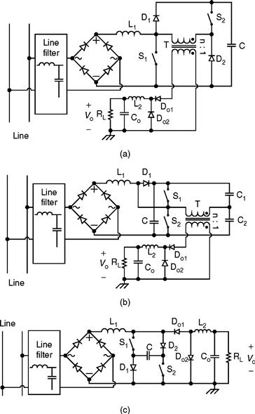
FIGURE 19.34 Two-switch single-stage power factor corrector: (a) boost–forward converter; (b) boost-half bridge converter; and (c) Sheppard–Taylor converter.
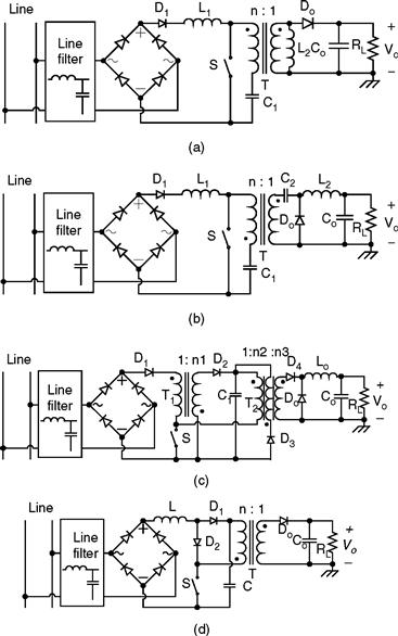
FIGURE 19.35 Single-stage single-switch PFC circuit: (a) boost–flyback combination circuit (BIFRED); (b) boost–buck combination circuit (BIBRED); (c) flyback–forward combination; and (d) boost–flyback combination.
Due to the simplicity and low cost, DCM boost converter is most commonly used for unity PF operation. The main drawback of using boost converter is that it shows considerable distortion of the average line current owing to the slow discharging of the inductor after the switch is turned off.
The output dc–dc converter can operate either in DCM or in CCM if small output ripple is desired. If the output circuit operates in CCM, there exists a power unbalance in S4-PFC converter when the load changes. Because the duty ratio is only sensitive to the output voltage in CCM operation, when the output power (output current) decreases, the duty ratio will keep unchanged. As both the input and the output circuit share the power switch, the input circuit will draw an unchanged power from the ac source. As a result, the input power is higher than the output power. The difference between the input power and the output power has to be stored in the storage capacitor, and hence increase in the dc bus voltage occurs. With the dc bus voltage’s rising, the duty ratio decreases. This process will be finished until a new power balance is built. As we can see, the new power balance is achieved at the penalty of increased voltage stress, resulting in high conduction losses in circuit components. Particularly, the high bus voltage causes difficulties in developing S4-converter for universal input (input line voltage rms value from ac 90 to 260 V) application.
Recent research on solving this problem can be found in [44–52]. The circuit in [44] uses two bulk capacitors that share the dc bus voltage change, shown in Fig. 19.36a. As a result, lower voltage is present at each of the capacitor. Reference [45] proposed a modified boost–forward PFC converter, in which a negative current feedback is introduced to the input circuit by the coupled windings of forward transformer, shown in Fig. 19.36b. In [46] a series resonant circuit called charge pump circuit is introduced into S4-PFC circuit, shown in Fig. 19.36c. As the load decrease, the charge pump circuit can suppress the dc bus voltage automatically.
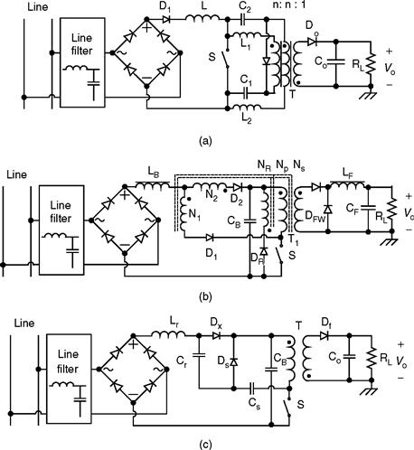
FIGURE 19.36 Improved S4-PFC converter: (a) boost–forward PFC circuit using two bulk capacitors; (b) boost–forward PFC circuit with reduced bus voltage; and (c) boost–flyback PFC circuit with charge pump circuit.
19.5.3 Other PFC Techniques
Extensive research in PFC continues to yield countless new techniques [15, 53–63]. The research topics are mainly focused on improvements of the PFC circuit performs such as fast performs, high efficiency, low cost, small input current distortion, and output ripple. The classification of PFC techniques presented here can only cover those methods that are frequently documented in the open literature. There are still many PFC methods which do not fall into the specified categories. The following are some examples:
• Second-harmonic-injected method [56]: In DCM input technique, even the converter operates at constant duty ratio, current distortion still exists. The basic idea of second-harmonic-injected method is compensating the duty ratio by injecting a certain amount of second harmonic into the duty ratio to modify the input I–V characteristic of the input converter. However, the output voltage may be affected by the modified duty ratio.
• Interleaved method [57]: An interleaved PFC circuit composed of several input converters in parallel. The peak input current of these converters follow the line voltage and are interleaved. A sinusoidal total line current is obtained by superimposing all the input current of the converters. The advantage of this method is that the converter input current can be easily smoothed by input EMI filter.
• Waveform synthesis method [58]: This method combines passive and active PFC techniques. Since the rectifier in the passive inductive-input PF corrector has a limited conduction angle, the input current is a single pulse around the peak of the line voltage, whereas the boost converter draws a non-zero current around the zero-cross of the line voltage. By controlling the operation mode of the active switch (enable and disable the boost converter at certain line voltage), the waveforms of active and passive PFC circuits are tailored to extend the conduction angle of the rectifier. The resulting current waveform has a PF greater than 0.9 and a THD lower than 20%.
19.6 Summary
To reduce losses, and decrease weight and size associated with converting ac power to dc power in linear power supply, switch mode power supplies (SMPSs) were introduced. The high non-linearity of this kind of power electronic systems handicaps itself by providing the utility power system with low power factor (PF) and high total harmonic distortion (THD). These unwanted harmonics are commonly corrected by incorporating power factor correction (PFC) technique into the SMPS. This chapter gives a technical review of current research in high frequency PFC, including the definition of PF and THD, configuration of PFC circuit, DCM input technique, and CCM shaping technique. The common issue of these techniques is to properly process the power flow so that the constant power dissipation at the output is reflected into ac power dissipation with two times the line frequency. Technically, PFC techniques encounter the following tradeoffs:
(a) Simplicity and accuracy: Single-stage PFC circuit has simple topology and simple control circuit, but has less control accuracy while two-stage PFC circuit has the contrary performance;
(b) Control simplicity and power handling capability: DCM input technique requires no input current control, but has less power handling capability while CCM has multiloop control and has more power handling capability;
(c) Switching frequency and conversion efficiency: To reduce weight and size of the PFC converter, higher switching frequency is desired. However, the associated switching losses result in decrease in conversion efficiency;
(d) Frequency response and bandwidth: To have good dynamic response, wider bandwidth is desired, however to achieve high PF bulk storage capacitor and output capacitor has to be used.
In the past decades, research in PFC techniques has led to the development of more efficient circuits and control strategies in order to optimize the design without compromising the above tradeoffs. Moreover, since the growth in power electronics strongly relies on the development of semiconductor devices, the recent advent of higher rating power devices, it is believed that the switching mode PF correctors will completely replace the existing passive reactive compensators in power system. In the distributed power system (DPS) where small size and high efficiency are of extreme importance, a new soft-switching technique has been used in designing PFC circuits. With the ever increasing market demanding for ultra-fast computer, the need for low output voltage (typically less than 1 V!) with high output currents and high efficiency converters has never been greater. Research efforts in developing high frequency high efficiency PFC circuits will continue to grow.
Acknowledgment
I would like to thank my doctoral students Guangyong Zhu, Shiguo Luo, and Wenkai Wu for their valuable contribution to the area of power factor correction.
Further Reading
1. Duffey CK, Stratford RP. Update of Harmonic Standard IEEE-519: IEEE Recommended Practices and Requirements for Harmonic Control in Electric Power Systems. IEEE Trans. on Industry Applications. Nov. 1989; vol. 25(no. 6):1025–1034.
2. Bose BK. Power Electronics –A Technology Review. Proceedings of the IEEE. Aug. 1992; 1303–1334.
3. Akagi H. Trends in Active Power Line Conditioners. IEEE Trans. on Power Electronics. May 1994; vol. 9(no. 3):263–268.
4. W. McMurray, “Power Electronics in The 1990’s,” Proceedings of IEEE-IECON’ 90, pp. 839–843.
5. McEachern A, Grady WM, Moncrief WA, Heydt GT, McGranaghan M. Revenue and Harmonics: An Evaluation of Some Proposed Rate Structures. IEEE Trans. on Power Delivery. Jan. 1995; vol. 10(no. 1):474–480.
6. Redl R, Tenti P, Van WYK JD. Power Electronics’ Polluting Effects. IEEE Spectrum. May 1997; 32–39.
7. J. S. Lai, D. Hurst, and T. Key, “Switch-Mode Power Supply Power Factor Improvement Via Harmonic Elimination Methods,” Conference Record of IEEE-APEC’ 91, pp. 415–422.
8. IEEE Inc., “IEEE Guide for Harmonic Control and Reactive Compensation of Static Power Converters (IEEE Std. 519-1981),” ANSI/IEEE Inc., 1981.
9. IEEE Inc., “IEEE Recommended Practices and Requirements for Harmonic Control in Electrical Power systems (IEEE Std. 519-1992),” ANSI/IEEE Inc., 1993.
10. I. Batarseh, “Power Electronic Circuits,” John Wiley & Sons Inc., (in press).
11. Tarter RE. Solid-State Power Conversion Handbook. John Wiley & Sons Inc. 1993
12. Vorperian V. Simplified Analysis of PWM Converters Using the Model of the PWM Switch: Parts I and II. IEEE Trans. on Aerospace and Electronic Systems. 1990; vol. 26(no. 3):490–505.
13. M. O. Eissa, S. B. Leeb, G. C. Verghese, and A. M. Stankovic, “A Fast Analog Controller for a Unity-Power-Factor AC/DC Converter,” Conference Record of APEC’ 94, pp. 551–555.
14. R. Liu, I. Batarseh, and C. Q. Lee, “Resonant Power Factor Correction Circuits with Resonant Capacitor-Voltage and Inductor-Current-Programmed Controls,” Conference Record of IEEE-APEC’ 93, pp. 675–680.
15. Y. Jiang and F. C. Lee, “Single-Stage Single-Phase Parallel Power Factor Correction Scheme,” Conference Record IEEE-PESC’ 94, pp. 1145–1151.
16. Dixon L. Average Current Mode Control of Switching Power Supplies. Product & Applications Handbook, Unitrode Integrated Circuits Corporation. 1993–94;U140:9-457–9-470.
17. Dixon L. High Power Factor Switching Preregulator Design Optimization. Unitrode Power Supply Design Seminar, Sem-1000. 1994; I3-1–I-12.
18. J. P. Noon andD. Dalal, “Practical Design Issues for PFC Circuits,” Conference Record of APEC’ 97, pp. 51–58.
19. Mammano B. Average Current-Mode Control Provides Enhanced Performance for a Broad Range of Power Topologies. PCIM’ 92-Power Conversion. Sep. 1992; 205–213.
20. Gegner JP, Lee CQ. Linear Peak Current Mode Control: A Simple Active Power Factor Correction Control Technique for Continuous Conduction Mode. Conference Record of IEEE-PESC’ 96. 1996; 196–202.
21. R. Redl and B. P. Erisman, “Reducing Distortion in Peak-Current-Controlled Boost Power-Factor Corrector” Conference Record of IEEE-APEC’ 94, pp. 576–583.
22. C. A. Caneson and I. Barbi, “Analysis and Design of Constant-Frequency Peak-Current-Controlled High-Power-Factor Boost Rectifier with Slope Compensation” Conference Record of IEEE-APEC’ 96, pp. 807–813.
23. A. R. Prasad, P. D. Ziogas, and S. Manias, “A New Active Power Factor Correction Method for Single-Phase Buck-Boost AC-DC Converter,” Conference Record of IEEE-APEC’ 92, pp. 814–820.
24. A. V. Costa, C. H. G. Treviso, and L. C. Freitas, “A New ZCS-ZVS-PWM Boost Converter with Unit Power Factor Operation,” Conference Record of IEEE-APEC’ 94, pp. 404–410.
25. J. Mahdavi, M. Tabandeh, and A. K. Shahriari, “Comparison of Conducted RFI Emission from Different Unity Power Factor AC/DC Converters” Conference Record of IEEE-PESC’ 96, pp. 1979–1985.
26. Salmon JC. Techniques for Minimizing the Input Current Distortion of Current-Controlled Single-Phase Boost Rectifiers. IEEE Trans. on Power Electronics. Oct. 1993; vol. 8(no. 4):509–520.
27. Srinivasan R, Oruganti R. A Unity Power Factor Converter Using Half-Bridge Boost Topology. IEEE Trans. on Power Electronics. May 1998; vol. 13(no. 3):487–500.
28. I. Barbi and S. A. Oliveira da Silva, “Sinusoidal Line Current Rectification at Unity Power Factor with Boost Quasi-Resonant Converters,” Conference Record of APEC’ 90, pp. 553–562.
29. Kazerani M, Ziogas PD, Joos G. A Novel Active Current Waveshaping Technique for Solid-State Input Power Factor Conditioners. IEEE Tans. on IE. Feb. 1991; vol. 38(no. 1):72–78.
30. H. Y. Wu, C. Wang, K. W. Yao and J. F. Zhang, “High Power Factor Single-Phase AC/DC Converter with DC Biased Hysteresis Control Technique,” Conference Record of APEC’ 97, pp. 88–93.
31. W. Tang, F. C. Lee, R. Ridley, and I. Cohen, “Charge Control: Modeling, Analysis and Design,” Conference Record of IEEE-PESC’ 92, pp. 503–511.
32. Tang W, Leu CS, Lee FC. Charge Control for Zero-Voltage-Switching Multiresonant Converter. IEEE Trans. on Power Electronics. Mar. 1996; vol. 11(no. 2):270–274.
33. R. Watson, G. C. Hua, and F. C. Lee, “Characterization of an Active Clamp Flyback Topology for Power Factor Correction Applications,” Conference Record of APEC’ 94, pp. 412–418.
34. D. Maksimovic, Y. Jang, and R. Erickson, “Nonlinear-Carrier Control for High Power Factor Boost Rectifiers,” Conference Record of APEC’ 95, pp. 635–641.
35. R. Zane and D. Maksimovic, “Nonlinear-Carrier Control for High-Power-Factor Rectifiers Based on Flyback, Cuk or Sepic Converters,” Conference Record of APEC’ 96, pp. 814–820.
36. H. Y. Wu, X. M. Yuan, J. F. Zhang, and W. X. Lin, “Single-Phase Unity Power Factor Current-Source Rectifiction with Buck-Type Input” Conference Record of IEEE-PESC’ 96, pp. 1149–1154.
37. R. Oruganti and M. Palaniapan, “Inductor Voltage Controlled Variable Power Factor Buck-Type Ac-Dc Converter,” Conference Record of IEEE-PESC’ 96, pp. 230–237.
38. S. M. Cuk, “Modeling, and Design of Switching Converters,” Ph.D. dissertation, California Institute of Technology, 1977.
39. R. Redl, L. Balogh, and N. O. Sokal, “A New Family of Single-Stage Isolated Power-Factor Correctors with Fast Regulation of the Output Voltage,” Conference Record of IEEE-PESC’ 94, pp. 1137–1144.
40. T. F. Wu, T. H. Yu, and Y. C. Liu, “Principle of Synthesizing Single-Stage Converters for Off-Line Applications,” Conference Record of IEEE-APEC’ 98, pp. 427–433.
41. M. Berg and J. A. Ferreira, “A Family of Low EMI, Unity Power Factor Correctors,” Conference Record of IEEE-PECS’ 96, pp. 1120–1127.
42. M. Madigan, R. Erickson, and E. Ismail, “Integrated High-Quality Rectifier-Regulators,” Conference Record of IEEE-PESC’ 92, pp. 1043–1051.
43. P. Kornetzky, H. Wei, and I. Batarseh, “A Novel One-Stage Power Factor Correction Converter,” Conference Record IEEE-APEC’ 97, pp. 251–258.
44. P. Kornetzky, H. Wei, G. Zhu, and I. Bartarseh, “A Single-Switch Ac/Dc Converter with Power Factor Correction,” Conference Record IEEE-PESC’ 97, pp. 527–535.
45. L. Huber and M. M. Jovanovic, “Single-Stage, Single-Switch, Isolated Power Supply Technique with Input-Current Shaping and Fast Output-Voltage Regulation for Universal Input-Voltage-Range Applications,” Conference Record IEEE-APEC’ 97, pp. 272–280.
46. J. Qian, Q. Zhao, and F. C. Lee, “Single-Stage Single-Switch Power Factor Correction (S4-PFC) AC/DC Converters with DC Bus Voltage Feedback for Universal Line Applications,” Conference Record of IEEE-Apec’ 98, pp. 223–229.
47. J. Qian and F. C. Lee, “A High Efficient Single Stage Single Switch High Power Factor AC/DC Converter with Universal Input,” Conference Record IEEE-APEC’ 97, pp. 281–287.
48. R. Redl, “Reducing Distortion in Boost Rectifiers with Automatic Control,” Conference Record of IEEE-APEC’ 97, pp. 74–80.
49. Y. S. Lee and K. W. Siu, “Single-Switch Fast-Response Switching Regulators with Unity Power Factor,” Conference Record of APEC’ 96, pp. 791–796.
50. M. M. Jovanovic, D. M. C. Tsang, F. C. Lee, “Reduction of Voltage Stress in Integrated High-Quality Rectifier-Regulators by Variable-Frequency Control,” Conference Record of APEC’ 94, pp. 569–575.
51. M. M. Jovanovic, D. Tsang, and F. C. Lee, “Reduction of Voltage Stress in Integrated High-Quality Rectifier-Regulators by Variable-Frequency Control,” Conference Record of APEC’ 94, pp. 569–575.
52. J. Wang, W. G. Dunford, and K. Mauch, “A Fixed Frequency, Fixed Duty Cycle Boost Converter with Ripple Free Input Inductor Current for Unity Power Factor Operation,” Conference Record of IEEE-PESC’ 96, pp. 1177–1183.
53. J. Sebastian, P. Villegas, F. Nuno, and M. M. Hernando, “Very Efficient Two-Input DC-to-DC Switching Post-Regulators,” Conference Record IEEE-PESC’ 96, pp. 874–880.
54. J. Sebastian, P. Villegas, M. M. Hernando, and S. Ollero, “Improving Dynamic Response of Power Factor Correctors by Using Series-Switching Post-Regulator,” Conference Record IEEE-APEC’ 98, pp. 441–446.
55. J. Hwang and A. Chee, “Improving Efficiency of a Pre-/Post-Switching Regulator (PFC/PWM) at Light Loads Using Green-Mode Function,” Conference Record IEEE-APEC’ 98, pp. 669–675.
56. D. Weng and S. Yuvarajan, “Constant-Switching Frequency AC-DC Second-Harmonic-Injected PWM,” Conference Record IEEE-APEC’ 95, pp. 642–646.
57. A. Miwa, D. M. Otten, and M. F. Schlecht, “High Efficiency Power Factor Correction Using Interleaving Techniques,” Conference Record IEEE-APEC’ 92, pp. 557–568.
58. M. S. Elmore, W. A. Peterson, and S. D., “A Power Factor Enhancement Circuit,” Conference Record IEEE-APEC’ 91, pp. 407–414.
59. J. Sebastian, P. Villegas, M. M. Hernando, and S. Ollero, “High Quality Flyback Power Factor Correction Based on a Two-Input Buck Post-Regulator,” Conference Record IEEE-APEC’ 97, pp. 288–294.
60. J. Rajagopalan, J. G. Cho, B. H. Cho, and F. C. Lee, “High Performance Control of Single-Phase Power Factor Correction Circuits Using a Discrete Time Domain Control Method,” Conference Record IEEE-APEC’ 95, pp. 647–653.
61. L. J. Borle and C. V. Nayar, “Ramptime Current Control,” Conference Record IEEE-APEC’ 96, pp. 828–834.
62. Dai SZ, Lujara NL, Ooi BT. A Unity Power Factor Current-Regulated SPWM Rectifier with a Notch Feedback for Stabilization and Active Filtering. IEEE Trans. on Power Electronics. Apr. 1992; vol. 7(no. 2):356–363.
63. Ohnuki T, Miyashita O, Haneyoshi T, Ohtsuji E. High Power Factor PWM Rectifiers with an Analog Pulsewidth Prediction Controller. IEEE Trans. on Power Electronics. May 1996; vol. 11(no. 3):460–471.
64. Zaninelli D, Domijan A. IEC and IEEE Standards on Harmonics and Comparisons. Proceedings of NSF Conf. on Unbundled Power Quality Services in Power Industry. Nov. 1996; 46–52.
65. Redl R. Power Factor Correction in Single-Phase Switching-Mode Power Supplies –an Overview. International Journal of Electronics. 1994; vol. 77(no. 5):555–582.
66. A. Prasada, P. D. Ziogas, and S. Manias, “A Novel Passive Waveshaping Method for Single-Phase Diode Rectifiers,” Conference Record of IEEE-PESC’ 89, pp. 99–105.
67. R. Redl and L. Balogh, “RMS, DC, Peak, and Harmonic Curent in High-frequency Power-Factor Correction with Capacitive Energy Storage,” Conference Record of IEEE-APEC’ 92, pp. 533–540.
68. E. P. Nowicki, “A Comparison of Single-Phase Transformer-Less PWM Frequency Changers with Unity Power Factor,” Conference record of IEEE-APEC’ 94, pp. 879–885.
69. Swamy MM, Bhat KS. A Comparison of Parallel Resonant Converters Operating in Lagging Power Factor Mode. IEEE Trans. on Power Electronics. Mar. 1994; vol. 9(no. 2):181–195.
70. Z. Lai, K. M. Smedley, and Y. Ma, “Time Quantity One-Cycle Control for Power Factor Correctors,” Conference Record IEEE-APEC’ 96, pp. 821–827.
71. Hong J, Maksimovic D, Erikson RW, Khan I. Half-Cycle Control of the Parallel Resonant Converter Operated as a High Power Factor Rectifier. IEEE Trans. on Power Electronics. Jan. 1995; vol. 10(no. 1):1–8.
72. Z. Lai and K. M. Smedley, “A Family of Power-Factor-Correction Controllers,” Conference Record of APEC’ 97, pp. 66–73.
73. J. Sun, W. C. Wu, and R. M. Bass, “Large-Signal Characterization of Single-Phase PFC Circuits with Different Types of Current Control,” Conference Record of IEEE-Apec’ 98, pp. 655–661.
74. Pomilio JA, Spiazzi G. High-Precision Current Source Using Low-Loss, Single-Switch, Three-Phase AC/DC Converter. IEEE Trans. on Power Electronics. July 1996; vol. 11(no. 4):561–566.
75. Dawande MS, Dubey GK. Programmable Input Power Factor Correction Method Rectifiers. IEEE Trans. on Power Electronics. July 1996; vol. 11(no. 4):585–591.
76. O. Garcia, C. P. Alou, R. Prieto, and J. Uceda, “A High Efficiency Low Output Voltage (3.3V) Single Stage AC/DC Power Factor Correction Converter,” Conference Record of IEEE-Apec’ 98, pp. 201–207.
77. K. Tse and M. H. L. Chow, “Single Stage High Power Factor Converter Using the Sheppard-Taylor Topology,” Conference Record of PESC’ 96, pp. 1191–1197.
78. M. Daniele, P. Jain, and G. Joos, “A Single Stage Single Switch Power Factor Correction AC/DC Converter,” Conference Record of PECS’ 96, pp. 216–222.
79. A. Canesin and I. Barbi, “A Unity Power Factor Multiple Isolated Outputs Switching Mode Power Supply Using a Single Switch,” Conference Record of APEC’ 91, pp. 430–436.
80. R. Erikson, M. Madigan, and S. Singer, “Design of a Simple High-Power-Factor Rectifier Based on the Flyback Converter,” Conference Record of APEC’ 90, pp. 792–801.
81. A. Peres, D. C. Martins, and I. Barbi, “Zeta Converter Applied in Power Factor Correction,” Conference Record of PESC’ 94, pp. 1152–1157.
82. J. Lazar and S. Cuk, “Feedback Loop Analysis for AC/DC Rectifiers Operating in Discontinuous Conduction Mode,” Conference Record of APEC’ 96, pp. 797–806.
83. J. Sebastián, P. Villegas, M. M. Herando, J. Diáz and A. Fantán, “Input Current shaper Based on the Series Connection of a Voltage Source and a Loss-Free Resistor,” Conference Record of IEEE-Apec’ 98, pp. 461–467.
84. A. Huliehel, F. C. Lee, and B. H. Cho, “Small-Signal Modeling of the Single-Phase Boost High Power Factor Converter with Constant Frequency Control,” IEEE PESC’ 92, pp. 475–482.
85. G. Zhu, H. Wei, P. Kornetzky, and I. Batarseh, “Small-Signal Modeling of a Single-Switch AC/DC Power Factor Correction Circuit,” IEEE PESC’ 98.
86. R. D. Middlebrook and S. Cuk, “A General Unified Approach to Modeling Switching Converter Stages,” IEEE PESC’ 76, pp. 18–31.
87. S. Tsai, “Small-Signal and Transient Analysis of a Zero-Voltage-Switched, Phase-Controlled PWM Converter Using Averaging Switch Model,” IEEE-IAS’ 91, pp. 1010–1016.
88. Dijk EV, Spruijt HJN, O’Sullivan DM, Klaassens JB. PWM-Switch Modeling of DC-DC Converter. IEEE Trans. on Power Electronics. Nov. 1995; vol. 10(no. 6):659–665.