
Oscillators
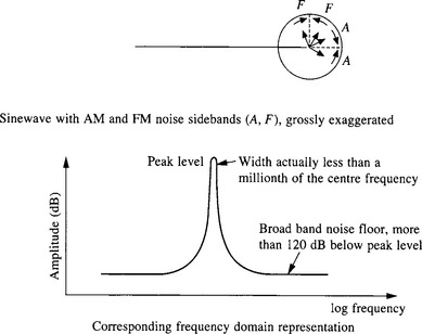
RF oscillators are used to produce the carrier wave which is required for a radio communications system. In the earliest days of ‘wireless communication’, spark transmitters were used; these produced bursts of incoherent RF energy containing a broad band of frequencies, although tuned circuits were soon introduced to narrow the band. However, valves and later transistors and FETs enable a single frequency oscillator to be produced. Typically, a tuned circuit is connected to the input of an amplifier, the output of which is coupled back into the tuned circuit. If it be arranged that at the resonant frequency of the tuned circuit, the gain from the input of the active device to its output, through the tuned circuit and back to its input again exceeds unity, then the inevitable small level of input noise of the active device will be amplified and will build up to a large continuous oscillation. The original noise will have been broadband, but the selectivity of the tuned circuit ensures that only the initial noise at the resonant frequency is amplified. Some mechanism is necessary to limit the amplitude of the oscillation and if one is not deliberately designed in then the circuit itself will provide it, for clearly the amplitude cannot go on building up for ever. Thus we have an oscillator with a steady output level at the frequency of the tuned circuit, plus the broadband noise of the device. The latter will still of course be there, though its level may be modified by the effect of the oscillator’s amplitude determining mechanism reducing the amplifier’s gain. The steady wanted output signal will in practice have very minor random amplitude and phase variations. The actual output can be resolved into an ideal output free of any amplitude or phase variations, plus random AM and PM noise sidebands: these fall off rapidly in amplitude with increasing offset from the wanted output frequency (Figure 9.1). The noise sidebands result in us being unable to predict at any instant exactly where in a ‘circle of confusion’ (much exaggerated in Figure 9.1) the tip of the vector is. The circle has no hard and fast boundary, the amplitude distribution with time of both the AM and FM noise sidebands exhibiting a normal or Gaussian distribution. In principle, the AM sidebands can be stripped off by passing the signal through a hard limiter, but any signal is necessarily accompanied by noise at thermal level or above and with a well-designed oscillator circuit, subsequent limiting will produce no significant reduction in AM noise sidebands. In any case, in most applications the PM noise sidebands are the most significant, as the most bandwidth-efficient modulation schemes (such as 8-ary PSK and others) are usually variants of phase modulation. The precise way in which the level of the PM sidebands drops off at increasing offsets from the carrier frequency depends upon a number of factors [1], but before considering this, note that an oscillator will also exhibit long-term frequency variations and these are best considered in the time domain.
Consider an oscillator circuit which is running continuously for a long period. Over a time scale of days to years there will be a gradual drift in the oscillator’s frequency, due to ageing of the components. For example, in an LC oscillator, it is difficult to produce an inductance with a long-term stability better than 1 part in 104. Where this is inadequate, a crystal oscillator may be used. The resonant frequency of a crystal will also drift with time. In the case of a solder-seal metal-can crystal the drift will usually be negative (falling frequency) due to the very small but finite vapour pressure of lead resulting in the deposition of lead atoms on the crystal. With cold-weld and glass-encapsulated types the drift is considerably less and may be either positive or negative. In the medium term, minutes to days, an oscillator will also exhibit frequency variations with changes in temperature due to the tempcos of the various components; here again crystal oscillators outperform LC types.
Returning to short-term variations, over periods of a few seconds or less, these are usually considered in the frequency domain as L(fm) dBC, the ratio of the single-sided phase noise power in a 1 Hz bandwidth to the carrier power (expressed in decibels), as a function of the offset-frequency (also called sideband-, modulation- or baseband-frequency) from the carrier. In practice, this is measured with a spectrum analyser, the result being the same whether the offset from the carrier at which the measurement is made be positive or negative, since the noise spectrum is symmetrical about the carrier (Figure 9.1). The following regions may be distinguished, moving progressively away from the carrier. At a very small offset fHz the power is proportional to f−4, i.e. a 12dB/octave roll-off (the random walk FM region); as f increases this changes to f−3 (−9dB/octave, flicker FM), then f−2 (−6 dB/octave, random walk phase), then f−1 (−3 dB/octave, flicker phase). The latter continues until the f0 region of flat far-out noise floor is reached: this cannot be less than −174 dBm (thermal in a 1 Hz bandwidth) and is typically −150 dBC or better. The breakpoints between the regions are gradual and where two are fairly close together, the corresponding region may not be observed at all. More details can be found in Reference 2.
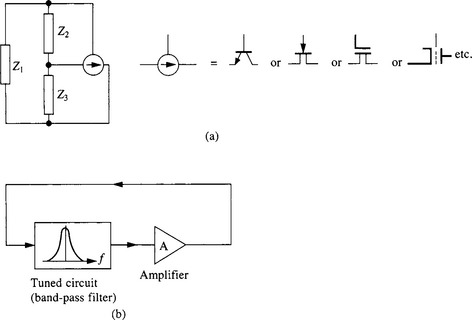
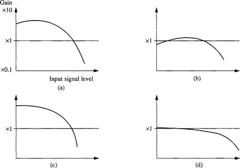
Turning to practical oscillators, Figure 9.2b shows a schematic filter/amplifier type oscillator, as described at the beginning of the chapter. Figure 9.2a shows a negative resistance type oscillator, examples being the Hartley and Colpitts circuits. In this type of oscillator, an active device is connected across a tuned circuit in such a way as to reflect a negative resistance −Rd in parallel with the tuned circuit, where Rd is the dynamic resistance of the tuned circuit. Thus the net losses are just made up, raising the effective Q to infinity at that particular level of oscillation. At lower levels, the negative resistance reflected across the tuned circuit is numerically lower, resulting in a loop gain exceeding unity, whilst at higher levels the negative resistance would be numerically greater than Rd, resulting in the losses in the tuned circuit exceeding the energy supplied by the active device. In practice, there is no real difference between the negative resistance and the filter/amplifier views of most oscillators, including those in Figure 9.2, but there are circuits, described later, which operate purely as negative resistance oscillators. Figure 9.3 shows plots of loop gain from the input of the amplifier to its output, through the filter (tuned circuit) and back again to the input, versus the input signal level to the amplifier. Characteristic 9.3c is typical of a well-designed oscillator: the loop gain at low levels exceeds unity by a comfortable margin and passes through unity at a steep angle. Such an oscillator is a sure-fire starter and the output level is very stable with low AM noise sidebands. Characteristic 9.3a is also met and is often acceptable, but 9.3b represents a totally unsatisfactory design. Such an oscillator will often start despite the less than unity small signal gain, due to the switch-on transient, but may fail to operate occasionally. Characteristic 9.3d represents an oscillator specially designed so that its gain changes only very gradually with level. Its amplitude of oscillation is consequently very susceptible to outside influences and such a circuit (coupled to a detector) will receive SW broadcast and amateur transmissions without an aerial of any sort connected when the loop gain is adjusted so that oscillation just commences, operating as a synchrodyne receiver.
The negative resistance oscillator of Figure 9.2a will only oscillate if Z2 and Z3 are reactances of the same sign and Z1 is of the opposite sign. Z1 capacitive gives the Hartley family of oscillators and Z1 inductive gives the Colpitts and its derivatives, the Clapp and Pierce oscillators. These are shown in Figure 9.4 along with sundry other types, including the TATG (tuned anode, tuned grid), so called from its valve origins. In the Clapp oscillator, noted for its good frequency stability, the additional capacitor C1 acts, together with C2 and C3, as a step-down transformer. This reduces the shunting effect on the tuned circuit of the input and output conductances and susceptances of the active device. Due to the light coupling of the active device to the tuned circuit, the arrangement requires an active device with a high mutual conductance, giving a large power gain. The dual-gate MOSFET electron-coupled oscillator is the solid state equivalent of the grounded screen valve tetrode circuit. (There is no solid state equivalent of the grounded cathode electron coupled oscillator, since that needs a pentode.) The electron-coupled circuit acts as both oscillator and buffer stage, variations of loading on the drain circuit having very little effect on the frequency.
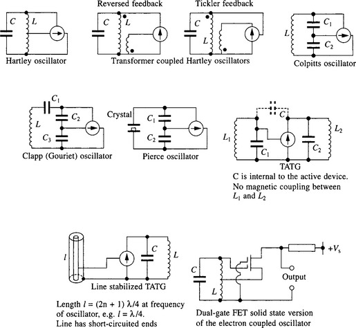
Figure 9.5 shows filter/amplifier oscillators of various sorts. The line-stabilized oscillator (like the line-stabilized TATG) is restricted to UHF and above, where a line of length equal to half a wavelength or more becomes a manageable proposition. At UHF, SAW delay lines can provide a delay of many cycles with little insertion loss and good stability. There is thus a ‘comb’ of frequencies at which they exhibit zero phase shift. A tuned circuit is required to select the desired frequency of oscillation: if the capacitor is a varactor, then one of a number of possible frequencies can be selected as required. Figure 9.6 shows oscillator circuits using two active devices. The greater maintaining-circuit power-gain available in the Franklin oscillator permits lighter coupling to the tuned circuit, reducing the pulling effect of stray maintaining circuit reactances. On the other hand, the additional device means that there is now another source of possible phase-shift variations round the loop. The emitter-coupled circuit of Figure 9.6b is unusual in that the tuned circuit operates at series resonance. It is thus suitable for a crystal operating at or near series resonance. This generally provides greater frequency stability than operation at parallel resonance, although the available pulling range is only about a tenth of that of a parallel-resonant crystal oscillator such as in Figure 9.4.
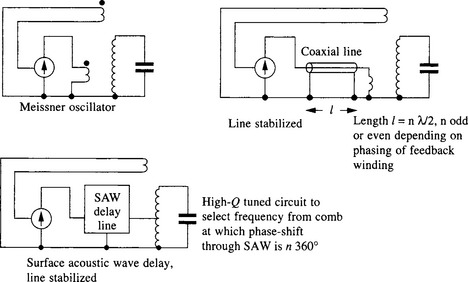
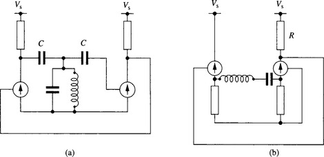
Figure 9.6 Two-device oscillators
(a) Franklin oscillator. The two stages provide a very high non-inverting gain. Consequently the two capacitors C can be very small and the tuned circuit operates at close to its unloaded value of Q
(b) Butler oscillator. This circuit is unusual in employing a series tuned resonant circuit. Alternatively it is suitable for a crystal operating at or near series resonance, in which case R can be replaced by a tuned circuit to ensure operation at the fundamental or desired harmonic, as appropriate
Figure 9.7a shows another oscillator circuit using two active devices, this time in push-pull. The two devices operate in antiphase but are effectively in parallel; it is not an emitter-coupled circuit. This arrangement elegantly solves one of the problems encountered with a single device bipolar transistor oscillator such as in Figure 9.4. In those circuits, the amplitude of oscillation usually increases until the net gain is brought down to unity by collector saturation imposing heavy damping on the tuned circuit at the negative peaks of collector voltage excursion (assuming an NPN implementation). It is usual to arrange that the resultant increase in base current biases the transistor back to a lower average collector current where the gain is also lower, but the increased damping is an undesirable (and usually the major) effect which stabilizes the amplitude. This effect did not arise in valve oscillators, the valve simply ceasing to conduct as the anode voltage fell towards or even below ground. (The same can be arranged with a bipolar transistor oscillator by connecting a high speed Schottky diode in series with the collector.) In the class D current switching oscillator, the fixed tail current is chopped into a squarewave, the fundamental component of which is selected by the tank circuit. For best frequency stability and output waveform, the tail current should be set at such a value that the transistors do not bottom. This means that in a wide range oscillator, one must either accept that the output amplitude will vary with frequency, or one must arrange to tune both L and C so as to maintain Rd constant, or the tail current must be varied with the tuning. The centre tap of the tank circuit may be connected directly to the decoupled positive supply, but in this case the centre tap to ground of the tuning capacitance is best omitted. Otherwise problems may arise if the inductor tap is not exactly at the electrical centre of the inductor − effectively giving two tuned circuits at slightly different frequencies. Grounding the centre point of the tuning capacitance is preferred since it provides a near short circuit to ground for the unwanted harmonic components of the device collector currents. These will be considerable, assuming the two resistors R are set to zero, as will usually be the case; the resistors may be added if desired to produce a characteristic approaching that in Figure 9.3d. If one of the two cross-coupling capacitors C is omitted, the circuit operates as an emitter-coupled negative-resistance oscillator, preserving some of the better characteristics of the original.
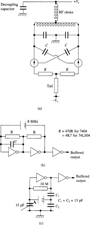
(a) Class D or current switching oscillator; also known as the Vakar oscillator. With R zero, the active devices act as switches, passing push–pull squarewaves of current. Capacitors C may be replaced by a feedback winding. R may be zero, or raised until circuit only just oscillates. ‘Tail’ resistor approximates a constant current sink
Figure 9.7b and c show two clock oscillators such as are used in microprocessor systems. The first operates at the series resonant frequency of the crystal; capacitor C provides some phase advance to compensate for the lag due to the propagation delay of the inverters. The second operates with the crystal near parallel resonance; component values will depend upon the operating frequency. In cost-sensitive applications the crystal can often be replaced by a ceramic resonator. In applications where frequency stability is the prime consideration, such as the frequency reference for a synthesizer, the rough and ready crystal oscillators of Figure 9.7 would be replaced by a TCXO (temperature-compensated crystal oscillator) or an OCXO (oven-controlled crystal oscillator). In the latter, the crystal itself and its maintaining circuit are housed within a container, the interior of which is maintained at a constant temperature higher than the highest expected ambient temperature, commonly at +75°C. An OCXO can provide a tempco of output frequency in the range 10−7−10−9 per °C, but stabilities substantially better than one part in 106 per annum are difficult to achieve with an AT cut crystal, although recent developments have improved on this to 1 in 109 per annum (typical), with phase noise already down to −140 dBc at only 10 Hz offset from the carrier. Figure 9.8a shows the typical cubic or ‘S’-shaped frequency variation of an AT cut crystal with temperature. The AT cut is ‘singly rotated’: one of the crystallographic axes lies along a diameter of the crystal blank but the orthogonal diameter of the blank is slightly offset from the orthogonal axis. By selecting the offset angle, the tempco at the point of inflection (which occurs at around 29°C) can be set anywhere from positive through zero to negative. It is thus possible in a non-temperature controlled oscillator to have a very low frequency variation with temperature over a rather limited range centred on 29°C, whilst if a larger temperature range must be covered then the angle of cut will be increased, leading to larger frequency variations with temperature. If an AT cut crystal is to be used in an OCXO, then again an increased angle of cut will be used, such as to place the upper turn-over point at the oven temperature (Figure 9.8a). The short- to medium-term stability of an OCXO is optimum when it is operated continuously. On the other hand, the long-term stability is then worse, since ageing is faster at oven temperature than at ambient. Figure 9.8b also shows the temperature variations of the BT and SC cuts in the region of the oven temperature. The SC (strain compensated) cut is doubly rotated, i.e. none of the three orthogonal crystallographic axes lies in the plane of the crystal blank. The SC cut is therefore more complicated to produce and hence more expensive than other types, but it offers improved resistance to shock and superior ageing performance. However, care in application is required, since the SC cut also exhibits more spurious resonance modes. For example, the 10 MHz SC crystal used in the Hewlett-Packard 10811A/B ovened reference oscillator is designed to run in the third overtone C mode resonance. The third overtone B mode resonance is at 10.9 MHz, the fundamental A mode resonance is at 7 MHz, and below that are the strong fundamental B and C modes. Figure 9.8c shows the SC cut crystal connected in what is basically a Colpitts oscillator, so as to provide the 180° phase inversion at the input of the inverting maintaining amplifier. With the correct choice of Lx, Ly and Cy, they will appear as a capacitive reactance over a narrow band of frequencies centred on the desired mode at 10 MHz, but as an inductive reactance at all other frequencies. Thus all the unwanted modes are suppressed [3].
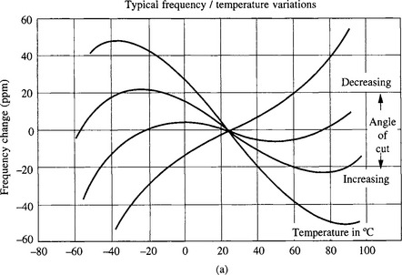
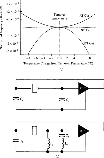
(a)Temperature characteristics of AT cut crystals
(b) Temperature performance of SC, AT and BT crystal cuts
(c) Standard Colpitts oscillator (top) and the same oscillator with SC mode suppression (10811A/B oscillator).
(Reproduced by courtesy of Agilent Technologies, www.agilent.com)
Where stability approaching that of an OCXO is necessary but the power drain of an oven or the time taken for it to warm up is unacceptable, then a TCXO may provide the solution. In this, the ambient temperature is sensed by one or more thermistors and a voltage with an appropriate law is derived for application to a voltage-controlled variable capacitor (varicap). Both OCXOs and TCXOs are provided with adjustment means – a trimmer capacitor or varicap diode controlled by a potentiometer – with sufficient range to cover several years drift, allowing periodic re-adjustment to the nominal frequency.
Before leaving the subject of oscillator circuits and turning to phase lock loops, a further word on negative resistance oscillators. It was mentioned that, as the active devices in the negative resistance oscillators of Figure 9.4 have all three electrodes connected to the tuned circuit, they could alternatively be considered as filter/amplifier circuits. However, there are other circuits which are truly negative resistance oscillators.
The losses in the tank circuit can be considered as a resistance, in parallel with a tuned circuit made with an ideal loss-free inductor and capacitor. If a resistance, equal in value to the loss resistance but opposite in sign, is connected in parallel, this ‘negative resistance’ exactly cancels out the loss resistance, and a steady oscillation will be maintained in the tank circuit. One suitable negative resistance device is the tunnel diode, and this can be used to make amplifiers or oscillators up to microwave frequencies. Unlike the transistor, it is strictly a two terminal device, but a circuit can also be devised such as to use a transistor as a true two-terminal negative resistance.
Figure 9.9a shows conventional current flowing into the emitter of a PNP transistor, and most of it coming out again at the collector. The ratio of the collector current to the emitter current is denoted by α, and is typically 0.99, and often even closer to unity. The base current Ib is the small difference between the emitter and collector current. Note that Ie = − (Ib + Ic) - from Kirchhoff’s first law. These relationships above apply at dc (0 Hz), and they also apply at low frequencies to small changes in current.
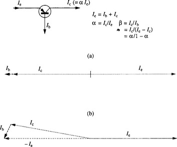
But at much higher frequencies, the current injected at the emitter has to travel through the base region before appearing at the collector. The result is that the collector current lags somewhat, as shown in the vector diagram, Figure 9.9b. But Ib + Ic must still equal −Ie, with the result that Ib must be as shown. Figure 9.11 shows a transistor with a capacitor Ce connected between its emitter and ground. If a small high frequency sinewave be connected to the transistor’s base terminal, then due to the high transconductance of a transistor, the emitter voltage will, to a first approximation, be the same as the base voltage. This voltage will appear across Ce, causing a leading current of magnitude determined by the reactance of Ce at the frequency concerned.
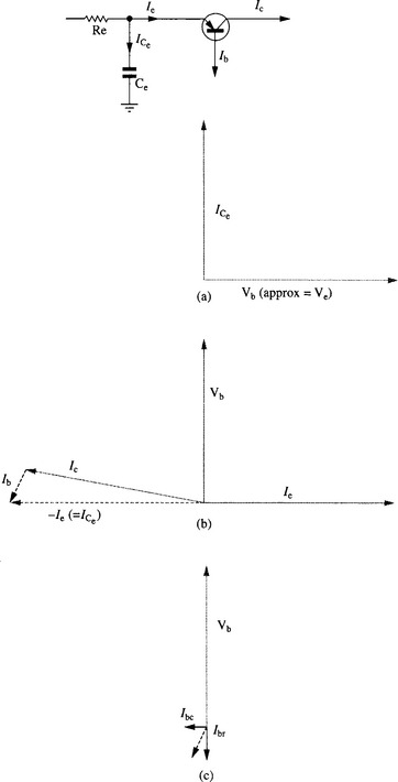
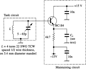
Figure 9.10a shows Ve (approximately equal to Vb), and the resultant current through Ce, which is the only emitter current, assuming that Re is very high, effectively a constant current generator. Clearly, ICe, must equal - Ie, since it is flowing away from the emitter, not into it. So rotating the vector diagram of Figure 9.10a by 90 degrees anticlockwise, and overlaying ICe on - Ie, Vb will appear as shown in Figure 9.10b.
Notice that Ib is almost in the opposite phase to Vb. Figure 9.10c shows it resolved into two components, a capacitive component Ibc in quadrature with Vb, and a resistive component Ibr. The current Ibr is in anti-phase with Vb; a negative resistance. Figure 9.11 shows an experimental 100 MHz negative resistance oscillator, a BC184 transistor with a capacitor from its emitter to ground, and its base connected to an LC tank circuit. Via this, the base is dc referenced to ground, while the Re of Figure 9.10 is 4K7. Due to the way the circuit works, as a two terminal negative resistance oscillator, the collector plays no part in circuit action, and is simply decoupled to ground.
With Ce a 3.9 pF capacitor, the oscillator covered 64-167 MHz. The output level to the spectrum analyser was +6 dBm over most of the range, falling to +4 dBm at 167 MHz and 0 dBm at 64 MHz.
Figure 9.12 shows the excellent spectral purity of the +6 dBm 100 MHz output, with the second harmonic 36 dB down on the fundamental, the third 48 dB down, the fourth 57 dB down and the fifth 70 dB down. Even better performance can be achieved by taking the output not from a tap on the coil as here, but via a grounded base transistor in the collector circuit, using the cascode connection.
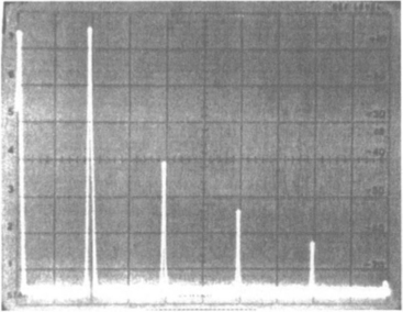
Figure 9.12 The output of the circuit of Figure 9.11, taken from a coil tapping at 3/4 turn up from ground. 10 db/div. vertical, top of screen reference level +10 dB, 50 MHz/div. horizontal, 0 Hz at left
For a general-purpose signal source such as a signal generator for the laboratory or test department, the traditional solution was an LC oscillator with switch selection of several ranges, accurately calibrated. Often a 1 MHz or 10 MHz crystal oscillator was incorporated, so that one of its harmonics could be used to check the scale calibration at the nearest 1 or 10 MHz point. Later, some signal generators were provided with ‘lock boxes’. Here, a variable ratio divider was set by the user to the appropriate setting for the RF output frequency of the signal generator, whose frequency was thus locked to that of the lock box’s crystal reference via the generator’s dc coupled external FM modulation input. In a still later development, the generator was equipped with a counter which both indicated the output frequency and provided the lock box setting, as in the legendary Hewlett-Packard 8640 series. When a LOCK button was pressed, a PLL (phase lock loop) was implemented as with the earlier separate lock boxes. It was not long before the operation of the PLL was entirely automated, making its operation transparent to the user. PLLs are now widely applied to frequency sources of all sorts in addition to signal generators, for example the local oscillators used in transmitters and receivers (see Chapter 11). Figure 9.13 shows the generic block diagram of a PLL and illustrates the operation of a first-order loop. A sample of the output of the VCO (voltage-controlled oscillator) is fed via a buffer amplifier to a variable ratio divider, e.g. ratio N. The divider output is compared with a comparison frequency fc, derived by dividing the output of a stable reference frequency source fref, such as a crystal oscillator, by a fixed reference divider ratio M. An error voltage is derived which, after smoothing, is fed to the VCO in such a sense as to reduce the frequency difference between the variable ratio divider’s output and the comparison frequency. If the comparison is performed by a frequency discriminator there will be a standing frequency error in the synthesizer’s output, albeit small if the loop gain is high. Such an arrangement is called a frequency lock loop (FLL); these are used in some specialized applications. However, the typical modern synthesizer operates as a PLL, where there is only a standing phase difference between the ratio N divider’s output and the comparison frequency. The oscillator’s output frequency is simply Nfc, where fc is the comparison frequency. Thus if fc were 12.5 kHz (Europe) or 15 KHz (USA) we would have a simple means of generating any of the transmit channel frequencies used in the VHF private mobile radio (PMR) band.
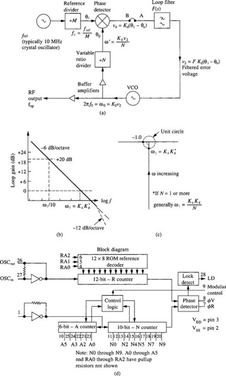
(a)Phase lock loop synthesizer
(b) Bode plot, first-order loop
(c) Nyquist diagram, first-order loop
(d) Block diagram of an LSI variable ratio N divider, with a counter to control a two modulus P.P + 1 prescaler, Motorola type MC145152.
(Copyright of Freescale Semiconductor, Inc. 2006, Used by permission)
In fact there is a practical difficulty in that variable ratio divide-by-N counters which work up to VHF or UHF frequencies were not available, but this problem was circumvented by the use of a prescaler. If a fixed prescaler ratio, say divide by 10, were used, then in the PMR example, the comparison frequency would have to be reduced to 1.25 kHz to compensate. However, the lower the comparison frequency, the more difficult it is to avoid comparison frequency ripple at the output of the phase comparator passing through the loop filter and reaching the VCO, causing comparison frequency FM sidebands. Of course we could just use a lower cut-off frequency in the filter, but this makes the synthesizer slower to settle to a new channel frequency following a change in N and also results in higher noise sidebands in the oscillator’s output. The solution is a two-modulus prescaler such as a divide by 10 or 11 type, usually written ÷10/11. Such prescalers are available in many ratios through ÷64/65 up to ÷512/514, providing a ‘fractional N’ facility so that a high comparison frequency can still be used. In the main loop divider chip there is, in addition to the programmable ÷ N counter, a programmable ÷ A prescalercontrol counter. After A input pulses to the main divider from the prescaler, the former’s prescaler-control line switches the prescale ratio from P + 1 to P, where it remains until the main divider has received N pulses, when the prescaler is switched back to ÷(P + 1). If A = 0 then the overall divide ratio Ntotal from the prescaler plus main divider is simply ÷ PN. For any value of A, every pulse out of the main divider will require A extra pulses into the prescaler, so that Ntotal = PN + A. Thus if A = N/2, then Ntotal = N(P + ![]() ), hence the term ‘fractional ratio divider’ for the combination of main and prescale counters. If A is set to zero, Ntotal = NP; if A = 1, Ntotal = NP + 1; if A = 2, Ntotal = NP + 2 and so on, up to A = (N − 1), giving Ntotal = NP + (N − 1). If now A were set to N, Ntotal would equal NP + N but this equals (N + 1)P, so instead A would be set back to zero, and N incremented by one instead. So effectively, N can be incremented in steps of unity, rather than in steps of P (see Figure 9.13d). Clearly, A must not be greater than N; also Ntotal; min = (P − 1)P + A and Ntotal;max = NmaxP + Amax. Other constraints will apply in any given situation, due to propagation times through the main and prescale counters and to the latter’s set-up and release times relative to its modulus control input.
), hence the term ‘fractional ratio divider’ for the combination of main and prescale counters. If A is set to zero, Ntotal = NP; if A = 1, Ntotal = NP + 1; if A = 2, Ntotal = NP + 2 and so on, up to A = (N − 1), giving Ntotal = NP + (N − 1). If now A were set to N, Ntotal would equal NP + N but this equals (N + 1)P, so instead A would be set back to zero, and N incremented by one instead. So effectively, N can be incremented in steps of unity, rather than in steps of P (see Figure 9.13d). Clearly, A must not be greater than N; also Ntotal; min = (P − 1)P + A and Ntotal;max = NmaxP + Amax. Other constraints will apply in any given situation, due to propagation times through the main and prescale counters and to the latter’s set-up and release times relative to its modulus control input.
A PLL synthesizer is an NFB loop and, as with any NFB loop, care must be taken to roll off all the loop gain safely before the phase shift reaches 180°. This is easier if the loop gain does not vary wildly over the frequency range covered by the synthesizer. Hence a VCO whose output frequency is a linear function of the control voltage is an advantage. The other elements of the loop also need to be correctly proportioned and the parameters of these have been marked in Figure 9.13a, following for the most part the terminology used in what is probably the best known treatise on phase lock loops [4]. Assuming that the loop is in lock, then both inputs to the phase detector are at the comparison frequency fc, but with a standing phase difference θi − θo. This results in a voltage υd out of the phase detector equal to Kd(θi − θo).
In fact, the phase detector output will usually include ripple at the comparison frequency or at 2fc, although there are phase detectors which produce very little (ideally zero) ripple. The ripple is suppressed by the low-pass loop filter, which passes υ2 (the dc component of υd) to the VCO. Assuming that the VCO’s output radian frequency ω0 is linearly related to υ2, then ω0 = K0υ2 = K0FKd(θi − θo), where F is the response of the low-pass filter. Because the loop is in lock, ω’ (i.e. ω0/N) is the same radian frequency as ωc, the comparison frequency. If the loop gain K0FKd/N is high, then for any frequency in the synthesizer’s operating range, θi − θo will be small. The loop gain must be at least high enough to tune the VCO over the frequency range without θi − θo exceeding ±90° or ±180°, whichever is the maximum range of the phase detector being used.
Let us check up on the dimensions of the various parameters, Kd is measured in volts per radian phase difference between the two phase detector inputs. F has units simply of volts per volt at any given frequency. K0 is in hertz per volt, i.e. radians per second per volt. Thus whilst the filtered error voltage υ2 is proportional to the difference in phase between the two phase detector inputs, υ2 directly controls not the VCO’s phase, but its frequency. Any change in frequency of ω0/N, however small, away from exact equality with ωref/M will result in the phase difference θi − θo increasing indefinitely with time. Thus the phase detector acts as a perfect integrator, whose gain falls at 6 dB per octave from an infinitely large value at dc. It is this infinite gain of the phase detector, considered as a frequency comparator, which is responsible for there being zero net average frequency error between the comparison frequency and fop/N. Consider a first order loop, i.e. one in which the filter F is omitted, or where F = 1 at all frequencies, which comes to the same thing. At some frequency ω1 the loop gain, which is falling at 6 dB/octave due to the phase detector, will be unity (0 dB). This is illustrated in Figure 9.13b and c, which shows the critical unity loop gain frequency ω1 on both an amplitude (Bode) plot and a vector (Nyquist) diagram. To find ω1 in terms of the loop parameters K0 and Kdwithout resort to the higher mathematics, we can notionally break the loop at B, the output of the phase detector, and insert at A a dc voltage exactly equal to that which was there previously. Now superimpose upon this dc level a sinusoidal signal, say a 1 V peak. The resultant peak FM deviation of ωo will be K0 rad/s. If the frequency of the superimposed sinusoidal signal were itself K0 rad/s, then the modulation index would be unity, corresponding to a peak VCO phase deviation of ±1 rad (see Chapter 8). This would result in a deviation of ± 1/N rad at the phase detector input and hence a detector output of Kd/N volts. If we change the frequency of the input at A from K0 to K0Kd/N, the peak VCO phase deviation will now be N/Kd. The deviation at the phase detector input is thus 1/Kd and so the voltage at B will be unity. So the unity loop gain frequency ω1 is K0Kd/N rad/s, as shown in Figure 9.13b and c. With a first order loop there is no independent choice of gain and bandwidth,quite simply ω1 = K0Kd/N. We could re-introduce the filter F as a simple passive CR cutting off at a corner frequency well above ω1, as indicated by the dotted line in Figure 9.13b and by the teacup handle at the origin in Figure 9.13c, to help suppress any comparison frequency ripple. This technically makes it a low-gain second-order loop, but it still behaves basically as a first-order loop provided the corner frequency of the filter is well clear of ω1 as shown.
Synthesizers usually make use of a high-gain second-order loop, which will be examined in a moment, but first a word as to why this type is preferred. Figure 9.14a compares the close in spectrum of a crystal oscillator with that of a mechanically-tuned LC oscillator and a VCO. Whereas the output of an ideal oscillator would consist of energy solely at the wanted output frequency f0, that of a practical oscillator is accompanied by undesired noise sidebands, representing minute variations in the oscillator’s amplitude and frequency. In a crystal oscillator these are very low, so the noise sidebands, at 100 Hz either side, are typically − 120 dB relative to the wanted output, falling to a noise floor further out of about −150 dB. The Q of an LC tuned circuit is only about one hundredth or less of the Q of a crystal, so the noise of a well-designed LC oscillator reaches −120 dB at more like 10 kHz off tune. In principle, a VCO using a varicap should not be much worse than a conventional LC oscillator provided the varicap diode has a high Q over the reverse bias voltage range, but with the high value of K0 commonly employed (maybe 10 MHz/V or more) noise on the control voltage line is a potential source of degradation. Like any NFB loop, a phaselock loop will reduce distortion in proportion to the loop gain. ‘Distortion’ in this context includes any phase deviation of ω’, and hence of ω0, from the phase of the comparison frequency. Thus over the range of offset from the carrier for which there is a high loop gain, the loop can clean up the VCO output to something more nearly resembling the performance of the reference, as illustrated in Figure 9.14b.
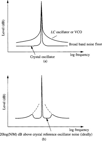
Figure 9.14 Purity of radio-frequency signal sources
(a) Comparison of spectral purity of a crystal and an LC oscillator
(b) At low–frequency offsets, where the loop gain is still high, the purity of the VCO (a buffered version of which forms the synthesizer’s output) can approach that of the crystal derived reference frequency, at least for small values of N/M
A second-order loop enables us to maintain a high loop gain up to a higher frequency, by rolling off the loop gain faster. Consider the case where the loop filter is an integrator as in Figure 9.15c; this is an example of a high-gain second-order loop. With the 90° phase lag of the active loop filter added to that of the phase detector, there is no phase margin whatever at the unity gain frequency; as Figure 9.15b shows, we are heading for disaster (or at least instability) at ω1where the loop gain is unity; ω1 = FK0Kd/N. By reducing the slope of the roll-off in Figure 9.15a to 6 dB/octave before the frequency reaches ω1 (dotted line), we can restore a phase margin, as shown dotted in Figure 9.15b, and the loop is stable. This is achieved simply by inserting a resistor R2 in series with the integrator capacitor C at X-Y in Figure 9.15c. This is the active counterpart of a passive transitional lag. If we make R1 = ![]() R2, then at the corner frequency of the filter ωf= 1/(CR2) the gain of the active filter is unity and its phase shift is 45°, whilst at higher frequencies it tends to − 3 dB and zero phase shift. If we make ωf equal to K0Kd/N, then ω1 (the loop unity gain frequency) is unaffected but there is now a 45° phase margin. It is convenient if K0, Kd and N are dimensioned so that the corresponding first-order loop unity-gain frequency ω1 = K0Kd/N is about one-tenth or less of the comparison frequency fc. Otherwise it becomes more difficult to avoid phase comparator ripple causing comparison frequency FM sidebands on the VCO output. If necessary, a comparator frequency notch filter can be included in the loop.
R2, then at the corner frequency of the filter ωf= 1/(CR2) the gain of the active filter is unity and its phase shift is 45°, whilst at higher frequencies it tends to − 3 dB and zero phase shift. If we make ωf equal to K0Kd/N, then ω1 (the loop unity gain frequency) is unaffected but there is now a 45° phase margin. It is convenient if K0, Kd and N are dimensioned so that the corresponding first-order loop unity-gain frequency ω1 = K0Kd/N is about one-tenth or less of the comparison frequency fc. Otherwise it becomes more difficult to avoid phase comparator ripple causing comparison frequency FM sidebands on the VCO output. If necessary, a comparator frequency notch filter can be included in the loop.
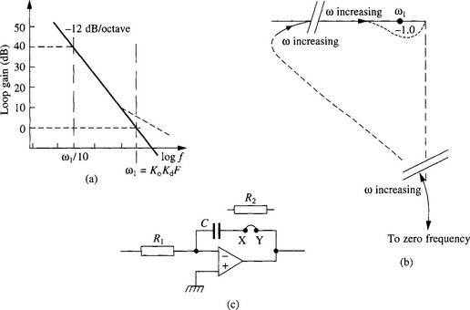
As Figure 9.15a shows, at frequencies well below ω1, the loop gain climbs at 12 dB/octave accompanied by a 180° phase shift, until the op-amp runs out of open loop gain. This occurs at the frequency ω where 1/(ωC) equals A times R1, where A is the open loop gain of the op-amp (an op-amp integrator only approximates a perfect integrator). Below that frequency, the loop gain continues to rise for evermore, but at just 6 dB/octave with an associated 90° lag, due to the phase detector which, as we noted, is a perfect integrator. This change occurs at a frequency too low to be shown in Figure 9.15a; it is off the page to the top left. It is only shown in Figure 9.15b by omitting chunks of the open-loop locus of the tip of the vector.
For a high-gain second-order loop, analysis by the root locus method [5] shows that the damping (phase margin) increases with increasing loop gain, so provided that the loop is stable at that output frequency (usually the top end of the tuning range) where K0 is smallest, then stability is assured. This is also clear from Figure 9.15. For if K0 or Kd increases, then so will ω1, the unity gain frequency of the corresponding first order loop. Thus ω1 is now higher than ωf (the corner frequency of the loop filter), so the phase margin will now be greater than 45°. Having found a generally suitable filter, let us return for another look at phase detectors and VCOs. Figure 9.16 shows several types of phase detector and indicates how they work. The logic types are fine for an application such as a synthesizer, but not so useful when trying to lock onto a noisy signal, e.g. from a distant, tumbling, spacecraft - here the EXOR type is more suitable, in conjunction perhaps with a third-order loop to give minimal frequency error with changing Doppler shift of the incoming signal. Both pump-up/pump-down and sample-and-hold types exhibit very little ripple when the standing phase error is very small, as is the case in a high-gain second-order loop. However the pump-up/pump-down types can cause problems. Ideally, pump-up pulses - albeit very narrow - are produced however small the phase lead of the reference with respect to the variable ratio divider output; likewise pump-down pulses are produced for the reverse phase condition. In practice, there may be a very narrow band of relative phase shift around the exactly in-phase point, where neither pump-up nor pump-down pulses are produced. The synthesizer is thus an entirely open loop until the phase drifts to one end or other of the ‘dead space’, when a correcting output is produced. Thus the loop acts as a ‘bang-bang’ servo, bouncing the phase back and forth from one end of the dead space to the other - evidenced by unwanted noise sidebands. Conversely, if both pump-up and pump-down pulses are produced at the in-phase condition, the phase detector is no longer ripple-free when in lock and, moreover, the loop gain may rise at this point. Ideally, the phase detector gain Kd should, like the VCO gain K0, be constant. Constant gain, and an absence of ripple when in lock, are the main attractions of the sample-and-hold phase detector. In the quest for low-noise sidebands in the output of a synthesizer, many ploys have been adopted. One very powerful aid is to minimize the VCO noise due to noise on the tuning voltage, by substantially minimizing K0, to the point where the error voltage can only tune the VCO over a fraction of the required frequency range. The VCO is pre-tuned by other means to approximately the right frequency, leaving the phaselock loop with only a fine tuning role. Figure 9.17 shows an example of this arrangement [6].
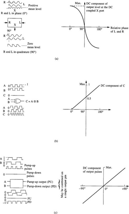
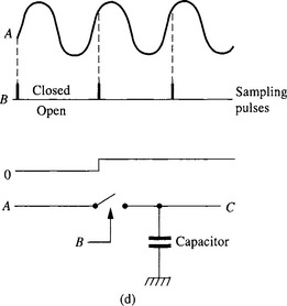
Figure 9.16 Phase detectors used in phase lock loops (PLLs)
(a) The ring DBM used as a phase detector is only approximately linear over say ±45° relative to quadrature
(b) The exclusive-OR gate used as a phase detector
(c) One type of logic phase detector
(d) The sample-and-hold phase detector. In the steady state following a phase change, this detector produces no comparison frequency ripple
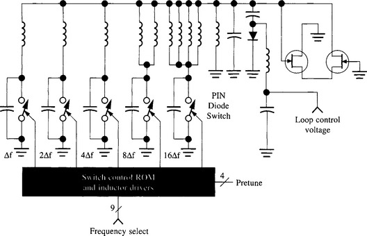
Figure 9.17 This VCO used in the HP8662A synthesized signal generator is pretuned to approximately the required frequency by the microcontroller. The PLL error voltage therefore only has to tune over a small range, resulting in spectral purity only previously attainable with a cavity tuned generator, and an RF settling time of less than 500μs. (Reproduced by courtesy of Agilent Technologies, www.agilent.com)
There are alternatives to the PLL approach to frequency generation. One of these is the direct synthesizer, pioneered by General Radio. A development of this system, using binary rather than decade increments in frequency resolution, was developed by Eaton Instruments (AILtech Division). In this scheme there is no effective frequency multiplication, as there is in a PLL. Instead, the required output frequency is built up by successively mixing selected harmonics of the very pure quartz crystal derived reference frequency, giving an output with levels of close-in noise not much worse than a crystal oscillator, and not approached by PLL type generators. However, owing to their very high cost, and subsequent improvements in PLL based synthesizers, direct synthesizers are no longer available. Another approach is DDS, direct digital synthesis - not to be confused with direct synthesis. In a DDS, a frequency setting number (held in a register) is repeatedly added into an accumulator at each occurrence of a clock pulse. The top N bits of the accumulator (where N is usually between 8 and 12) are used to address a sine look-up ROM (read-only memory), the output values from which are passed to a DAC (digital to analog converter). Thus the latter outputs a stepwise approximation to a sinewave, each cycle corresponding to one pass through the ROM address range. An advanced implementation, using an arrangement needing just a quarter of a sinewave stored in ROM, is shown in Figure 9.18. At exceedingly low frequencies, the level corresponding to each ROM location may be output during two or more successive clock periods. This occurs when the number in the frequency setting register includes no ‘ones’ in the top N bits. On the other hand, at much higher frequencies, only a subset of ROM locations would be visited in one cycle of the output, a different subset usually applying in successive cycles. This gives rise to unwanted frequency components in the output; these may appear either as a few isolated spectral lines, or - for frequencies totally unrelated to the clock frequency - as a sea of low level spurs approximating to a raised noise floor. The cleanest output occurs when the selected frequency is a binary whole number, i.e. a power of 2 submultiple of the clock frequency; there are then no line spurs (other than harmonics of the output frequency), and the output is as pure as the clock frequency, possibly better, due to the division. At a small offset from such a frequency, close-to-carrier spurs will typically appear, the spacing being dependent upon the submultiple. For instance, at an output frequency offset by 1 kHz from f/4, spurs would appear at ±4 kHz.
Figure 9.18 SP2002 direct frequency synthesizer block diagram. This device, which was available in selections operating up to a clock frequency of 2.5 GHz, is now discontinued, but the architecture is typical of direct digital synthesizers. (Reproduced by courtesy of Zarlink Semiconductor Ltd. www.zarlink.com)
The maximum output frequency from some DDS chips can be as high as one-third of the clock frequency or more, but in some designs (e.g. Figure 9.18) is limited by the architecture of fclock/4. If working up towards the Nyquist frequency of fclock/2, filtering will be required to suppress spurious outputs at image frequencies above the Nyquist rate. Figure 9.19a shows the output waveform of a DDS clocked at 400 MHz and set to provide an output frequency of 62.5 MHz, i.e. 5/32ths of the clock frequency. A different subset of levels (corresponding to ROM addresses) appears at subsequent cycles, the pattern recurring exactly after each fifth cycle. Thus, in the strict sense, the output is actually a 12.5 MHz signal, but with the fifth harmonic much stronger than the fundamental or any other harmonic, as can be seen on a spectrum analyser (Figure 9.19b). At more abstruse ratios than 5/32, many more spurious lines appear, but the total spurious power tends to remain roughly constant, so their levels are generally lower. As a DDS is ‘tuned’ across its range, by incrementing the frequency setting word, various of the spurious outputs actually move through the wanted output frequency. Clearly, when this happens, they cannot be separated by filtering; in many cases this limits the applicability of DDS.
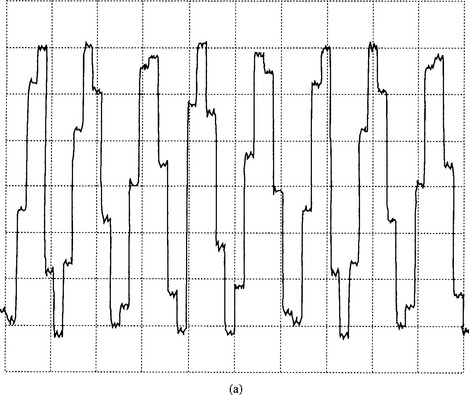
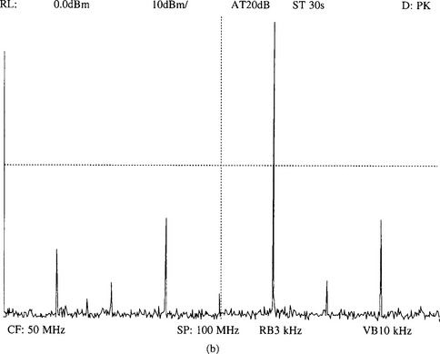
Figure 9.19 Output of a direct digital synthesizer in the time and frequency domains
(a)Output of a DDS clocked at 400 MHz and set to fout = 62.5 MHz. (The wiggles on the steps are an artefact of the digital storage oscilloscope used)
(Reproduced with permission from ‘Direct digital synthesis, aspects of operation and application,’ by D. May, IEE Electronics Division Colloquium on Direct Digital Frequency Synthesis, November 1991, Digest No. 1991/172)
However, a hybrid system may provide the answer (Figure 9.20). When the output of a DDS is set to one-quarter or less of the clock frequency, one can find frequency bands of width up to a few tenths of 1% of the clock frequency over which all spurious outputs are more than 80 dB down on the wanted output, although there may be spurs outside such a band. If the DDS operation is centred on 10.7 MHz, a highly selective crystal filter (such as used in PMR applications) can pick out a spurious free signal which may be set anywhere within the filter’s bandwidth. With a reference frequency division ratio M of 5, the loop operates with a comparison frequency in excess of 2 MHz. This has two major benefits: firstly, a high loop gain may be retained up to a much higher frequency than normal, avoiding the rise in noise outside the loop bandwidth visible as ‘ears’ in Figure 9.14b and, secondly, the wide loop bandwidth results in very rapid settling following a change to a new frequency. The degree of resolution of the DDS, which typically has 30 or more bits in the frequency setting word, is so great that the synthesizer’s output may be varied between the steps of the main loop in increments as small as 1 Hz or less. Note that this scheme provides its fine resolution by adjusting the frequency of the reference. The consequence of this is that the size of the fine loop steps is not constant, but proportional to the main loop divider ratio N. Thus, for a given synthesizer output frequency, the setting of the DDS must be calculated taking N into account, but this is no problem in a modern microprocessor-controlled design. Whilst the DDS of Figure 9.14, clocked at 2.5 GHz, was capable of providing output frequencies up to 625 MHz directly, this was exceptional. Typically the maximum output frequency available from most DDS chips is limited to a few hundred MHz, if that. However, ‘the baseband’ output spectrum, from 0 Hz up to Nyquist rate of fclock/2, appears mirrored each side of the clock frequency and its harmonics, and a signal from one of these sidebands may be used to provide an output up to several times the Nyquist rate. The down side is that the baseband and sideband spectra are subject to a sin(x)/x amplitude distribution, and consequently these higher order outputs exhibit a lower ratio of wanted output to spurious plus noise components.
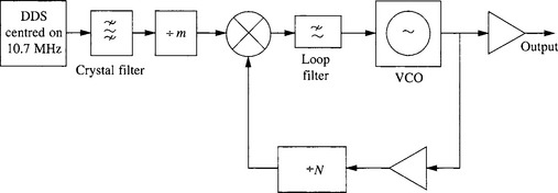
Figure 9.20 Hybrid DDS/PLL synthesizer (Reproduced with permission from ‘Direct digital synthesis, aspects of operation and application,’ by D. May, IEE Electronics Division Colloquium on Direct Digital Frequency Synthesis, November 1991, Digest No. 1971/172)
References
1. Robins, W. P. Phase Noise in Signal Sources, IEE Telecommunications Series: 9 Peter Peregrinus
2. Scherer, D. Design principles and test methods for low phase noise RF and microwave sources. RF and Microwave Measurement Symposium, Hewlett-Packard
3. March, Burgoon, J.R., Wilson, R.L. SC-cut quartz oscillator offers improved performance. Hewlett-Packard Journal, 1981;32(3):20.
4. Gardner, F.M. Phaselock Techniques, New York, John Wiley, 1966.
5. Truxal, J.G. Automatic Feedback Control System Synthesis, New York, McGraw-Hill, 1955.
6. February, Sherer, Chan, Ives, Crilly, Mathiesen. Low-noise RF signal generator designs. Hewlett-Packard Journal, 1981;32(2):12.