9
Electronic Systems Reliability
9.1 Introduction
Reliability engineering and management grew up largely in response to the problems of the low reliability of early electronic equipment, and many of the techniques have been developed from electronics applications. The design and construction of an electronic system, more than any other branch of engineering, involves the utilization of very large numbers of components which are similar, but over which the designer and production engineer have relatively little control. For example, for a given logic function a particular integrated circuit device might be selected. Apart from choosing a functionally identical device from a second source, the designer usually has no option but to use the catalogued item. The reliability of the device used can be controlled to a large extent in the procurement and manufacturing phases but, as will be explained, mainly by quality control methods. The circuit designer generally has little control over the design reliability of the device. This trend has become steadily more pronounced from the time that complex electronic systems started to be produced. As the transistor gave way to the integrated circuit (IC) and progressively with the advent of large scale integration (LSI) and very large scale integration (VLSI), the electronic system designer's control over some of the major factors influencing reliability has decreased. However, this is changing in some respects as system designs are increasingly implemented on custom-designed or semi-custom integrated circuits. This aspect is covered in more detail later. This is not to say that the designer's role is diminished in relation to reliability. Rather, the designer of an electronic system must be, more than in most other branches of engineering, a member of a team, involving people from other technologies, production, quality control, test planning, reliability engineering and others. Without such a team approach, his or her functionally correct design could be highly unreliable. It is less likely that the designer of a functionally correct hydraulic or mechanical system could be as badly let down. It is important to understand the reasons for this difference.
For the great majority of electronic components and systems the major determinant of reliability is quality control of all of the production processes. This is also true of non-electronic components (subject in both cases to the items being used within specification). However, most non-electronic equipment can be inspected and tested to an extent sufficient to assure that they will operate reliably. Electronic components cannot be easily inspected, since they are nearly always encapsulated. In fact, apart from X-ray inspection of parts for ultra-high reliability products, internal inspection is not generally possible. Since electronic components, once encapsulated, cannot be inspected, and since the size and quantity of modern components dictates that very precise dimensions be held at very high production rates, it is inevitable that production variations will be built into any component population. Gross defects, that is, failure to function within specification, can easily be detected by automatic or manual testing. However, it is the defects that do not immediately affect performance that are the major causes of electronic component unreliability.
Consider a typical failure mechanism in an electronic component: a weak mechanical bond of a lead-in conductor to the conducting material of the device. This may be the case in a resistor, a capacitor, a transistor or an IC. Such a device might function satisfactorily on test after manufacture and in all functional tests when built into a system. No practical inspection method will detect the flaw. However, because the bond is defective it may fail at some later time, due to mechanical stress or overheating due to a high current density at the bond. Several other failure mechanisms lead to this sort of effect, for example, flaws in semiconductor material and defective hermetic sealing. Similar types of failure occur in non-electronic systems, but generally they do not predominate.
The typical ‘electronic’ failure mechanism is a wearout or stress induced failure of a defective item. In this context, ‘good’ components do not fail, since the application of specified loads during the anticipated life will not lead to failure. While every defective item will have a unique life characteristic, depending upon the nature of the defect and the load(s) applied, it is possible to generalize about the nature of the failure distributions of electronic components. Taking the case of the defective bond, its time to failure is likely to be affected by the voltage applied across it, the ambient temperature around the device and mechanical loading, for example, vibration. Other failure mechanisms, say a flaw in a silicon crystal, may be accelerated mainly by temperature variations. Defects in devices can result in high localized current densities, leading to failure when the critical value for a defective device is exceeded.
Of course, by no means all electronic system unreliability is due to defective components. Interconnects such as solder joints and wire bonds can be reliability ‘weak links’ especially in harsh environment applications (automotive, avionics, military, oil drilling, etc.). Other failure mechanisms will be described later in this chapter.
Also the designer still has the task of ensuring that the load applied to components in the system will not exceed rated (or derated values), under steady-state, transient, test or operating conditions. Since electronic component reliability can be affected by temperature, design to control temperatures, particularly localized ‘hot spots’, is necessary. Thus the designer is still subject to the reliability disciplines covered in Chapter 7.
Electronic system failures can be caused by mechanisms other than load exceeding strength. For example, parameter drifts in components, short circuits due to solder defects or inclusions in components, high resistance relay or connector contacts, tolerance mismatches and electromagnetic interference are examples of failures which may not be caused by load. We will consider these failure modes later, appropriate to the various components and processes which make up electronic systems.
9.2 Reliability of Electronic Components
Electronic components can be caused to fail by most of the same mechanisms (fatigue, creep, wear, corrosion, etc.) described in the previous chapter. Fatigue is a common cause of failure of solder joints on surface mounted components and on connections to relatively heavy or unsupported components such as transformers, switches and vertically mounted capacitors. Wear affects connectors. Corrosion can attack metal conductors on integrated circuits, connectors and other components. Electrical and thermal stresses can also cause failures that are unique to electronics. The main electrical stresses that can cause failures of electrical and electronic components and systems are current, voltage and power. For all of these failure modes there are strong interactions between the electrical and thermal stresses, since current flow generates heat.
It is important to appreciate the fact that the great majority of electronic component types do not have any mechanisms that will cause degradation or failure during storage or use, provided that they are:
- Properly selected and applied, in terms of performance, stress and protection.
- Not defective or damaged when assembled into the circuit.
- Not overstressed or damaged in use.
The quality of manufacture of modern electronic components is so high that the proportions that might be defective in any purchased quantity are typically of the order of less than ten per million for complex components like ICs, and even lower for simpler components. Therefore the potential reliability of well-designed, well-manufactured electronic systems is extremely high, and there are no practical limits to the reliability that can be achieved with reasonable care and expenditure.
9.2.1 Stress Effects
9.2.1.1 Current
Electrical currents cause the temperatures of conductors to rise. If the temperature approaches the melting point, the conductor will fuse. (Of course fuses are used as protective devices to prevent other, more serious failures from occurring.) Heat in conductors is transferred to other components and to insulation materials, primarily by conduction and convection, so thermal damage can be caused to these.
High currents can also cause component parameter values, such as resistance, to drift over time. This effect is also accelerated by high operating temperatures. Figure 9.1 shows an example of this.
Electric currents also create magnetic fields. If oscillating, they can generate acoustic noise and electromechanical vibration. We will discuss electrical interference effects later.
9.2.1.2 Voltage
Voltage stress is resisted by the dielectric strength of the material between the different potentials. The most common examples are the dielectric material between capacitor plates, and the insulation (air or other insulator) between conductors. Potential differences generate currents in conductors and components, and if the current carrying capacity is insufficient the conductor or component will fail, in which case the failure mechanism is current, though the cause might be that the voltage is too high. For example, an integrated circuit might fail due to current overstress if a high electrostatic voltage is accidentally applied to it, and a 110 V appliance might fail for the same reason if connected to a 240 V supply.
High voltage levels can be induced by:
- Electrostatic discharge (ESD), caused by charge accumulation on clothing, tools, and so on.
- Other electrical overstress, such as high voltage transients on power lines, unregulated power supplies, circuit faults that lead to components being overstressed, accidental connection of high voltages to low power components, and so on. This is referred to as electrical overstress (EOS).
Another effect of voltage stress is arcing, which can occur whenever contacts are opened, for example in switches and relays. Arcing can also occur between brushes and commutators of motors and generators. Arcing generates electromagnetic noise, and also progressively damages the contact surfaces, leading eventually to failure. Arcing can also cause damage to electric motor bearings, if they provide a current path due to inadequate design or maintenance.
Arcing can be reduced by using voltage suppression components, such as capacitors across relay or switch contacts. Arcing becomes more likely, and is more difficult to suppress, if atmospheric pressure is reduced, since the dielectric constant of air is proportional to the pressure. This is why aircraft and spacecraft electrical systems operate at relatively low voltage levels, such as 28 V DC and 115 V AC.
Corona discharge can occur at sharp points at moderate to high voltage levels. This can lead to dust or other particles collecting in the area, due to ionization.
Some components can fail due to very low or zero current or voltage application. Low-power relay contacts which pass very low DC currents for long periods can stick in the closed position due to cold welding of the contact surfaces. Electrical contacts such as integrated circuit socket connectors can become open due to build-up of a thin dielectric layer caused by oxidation or contamination, which the low voltage stress is unable to break down.
9.2.1.3 Temperature
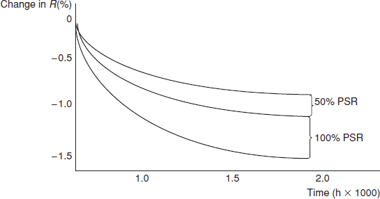
The Arrhenius formula that relates physical and chemical process rates to temperature has been used to describe the relationship between temperature and time to failure for electronic components, and is the basis of methods for predicting the reliability of electronic systems, as described in Chapter 6. However, this is sometimes an erroneous application, since, for many modern electronic components, most failure mechanisms are not activated or accelerated by temperature increase. The materials and processes used are stable up to temperatures well in excess of those recommended in component manufacturers’ application specifications. The reason why the relationship seemed to hold was probably because, in the early years of microcircuit technology, quality control standards were not as high, and therefore a fairly large proportion of components were observed to fail at higher temperatures. However, current data do not show such a relationship, except for some specific failure modes which will be described later. This has major implications for thermal design, since the erroneous impression that ‘the cooler the better’ is widely held.
The true relationship between temperature and failure is as shown in Figure 9.2. Most electronic components can be applied at temperatures well in excess of the figures stated in databooks. For example, databook package temperature limits for industrial grade plastic encapsulated integrated circuits and transistors are typically 85 °C, and for ceramic or metal packaged devices 125 °C. These do not, however, relate to any physical limitations, but are based more on the conventions of the industry.
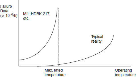
Figure 9.2 Temperature vs. reliability for electronic components.
Low temperatures can cause components to fail, usually due to parametric changes in electrical characteristics. Typical low temperature limits for most components are −20 °C to −60 °C. However, such failures are usually reversible, and correct function is regained if the temperature rises.
Repeated temperature changes can be more damaging than continuous operation at high temperatures. Temperature changes also cause fatigue damage and creep deformation of solder joints on surface-mounted electronic components, as described in Chapter 8.
9.2.1.4 Power
Electrical power generates heat (W = I2 R). All ‘active’ electronic components, such as transistors, integrated circuits and amplifiers generate heat, and therefore increased temperature. So do components like coils, voltage dropping resistors, and so on. The steady-state component temperature will be the sum of the ambient temperature and the temperature generated by internal heating. The internal heat is dissipated by conduction through the device connections and mountings, and the thermal resistance between the active part of the device and the ultimate heat sink will determine the steady-state temperature. We discussed the effects of temperature on electronic device reliability earlier.
Some passive devices, such as resistors and capacitors, are also susceptible to failure due to power stress, if it causes overheating (rather than fusing due to excess current). Power stress over long periods can also cause drift of parameter values such as resistance or capacitance. Application instructions for such components generally include power stress limits.
Power stress cycling can lead to failure due to induced thermal cycling and thus fatigue, as described earlier.
9.3 Component Types and Failure Mechanisms
The main categories of electronic component types and their most common failure mechanisms are described in the sections below.
9.3.1 Integrated Circuits (ICs)
Integrated circuits (ICs) are not really ‘components’. They are in fact sub-systems, containing transistors, capacitors and other discrete components within the IC structure. In the past ICs have been classified as follows: small scale integration (SSI): up to 100 logic gates; medium scale integration (MSI): up to 1000 gates; large scale integration (LSI): up to 10 000 gates; very large scale integration (VLSI): more than 10 000 gates, although those classifications are not used as often these days. Currently (2011) microprocessors can contain several billion (109) transistors.
Construction of ICs starts with the selective diffusion into the silicon wafer of areas of different charge level, either by ionic diffusion in a furnace or by implantation by a charged particle accelerator. The latter method is used for large-scale production. In the diffusion process, the areas for treatment are defined by masks. A sequence of treatments, with intermediate removal by chemical etch of selected areas, creates the structure of transistors and capacitors.
Different layers of the diffusion process are electrically isolated by layers of silicon dioxide (SiO2). This is called passivation. Finally, the entire die surface, apart from connector pads for the wire bonds, is protected with a further SiO2 or Si3N4 layer. This process is called glassivation.
The connections between transistors on the chip and to the input and output pins are made via a network of conductor tracks, by depositing a thin layer of metal (metallization) on to the surface, through a mask. More recently, the number of interconnect levels has substantially increased due to the large number of transistors. Therefore, the timing delay in the wiring has become significant prompting a change in wiring material from aluminium to copper and from the silicon dioxides to materials with lower dielectric constant. Examples of these materials (called low-K dielectrics) include SiO2 doped with fluorine or with carbon.
Finally, the assembly is packaged in either a plastic moulding or in a hermetic (ceramic or metal) package.
When ICs were first produced in the 1970s and 1980s they were mainly fairly simple analogue and digital circuits with defined functions (op-amps, adders, flip-flops, logic gates, etc.), and they were produced to closely defined generic specifications. For example, a 7408 is a 2-input AND gate, and it might have been manufactured by several suppliers. In parallel with the rapid growth in complexity and functionality in the years since, several different classes of IC have been developed. The classes that are available today include:
- ‘Standard’ ICs. These are the components that appear in generic specifications or in manufacturers’ catalogues. Examples are logic, memories, microprocessors, analogue to digital converters, signal processing devices, op-amps, and so on.
- Programmable logic devices (PLDs), field programmable gate arrays (FPGAs). These are standard circuits which can be ‘programmed’ by selective opening of fusible links.
- Mixed signal ICs. These have both digital and analogue circuits integrated into the same chip.
- Microwave monolithic ICs (MMICs). These are used in systems such as telecommunications, and contain microwave radio circuits.
- Complex multifunction devices (also referred as system on a chip (SOC)), which might contain mixed technologies, such as processing, memory, analogue /digital conversion, optical conversion, and so on, and a mixture of new and ‘legacy’ circuit designs.
- Micro-electro-mechanical systems (MEMS) is the technology of very small mechanical devices driven by electricity. MEMS are also referred to as micromachines in Japan, or Micro Systems Technology (MST) in Europe. Materials used for MEMS manufacturing include silicon, polymers and various metals, such as gold, nickel, aluminium, copper, and so on MEMS applications include sensors, actuators, medical devices and many others.
9.3.1.1 Application-Specific ICs
There is an increasing trend for ICs to be designed for specific applications. Standard ICs such as microprocessors and memories will always be used, but many circuits can be more economically implemented by using ICs which have been designed for the particular application. These are called application-specific ICs (ASICs).
In a semi-custom ASIC, all fabrication processes on the chip are previously completed, leaving arrays of transistors or cells to be interconnected by a conductor pattern designed for the particular application. In a full custom design, however, the chip is designed and manufactured entirely for the specific application.
Semi-custom ASICs are more economical than full custom ICs in relatively low quantities, but there is less flexibility of design and the utilization of chip area is less economical. Full custom ASICs are usually economical when large quantities are to be used, since the design and development costs are high. Both design approaches rely heavily on EDA, though the semi-custom method is easier to implement.
ASICs introduce important reliability aspects. The electronic system designer is no longer selecting ‘black boxes’, that is, standard ICs, from a catalogue, but is designing the system at the component (or functional group) level. Reliability (and testability) analysis must be performed to this level, not just to input and output pins. Since design changes are very expensive, it is necessary to ensure that the circuit is reliable and testable the first time. Particular aspects that need to be considered are:
- Satisfactory operation under the range of operating inputs and outputs. It is not usually practicable to test a LSI or VLSI design exhaustively, due to the very large number of different operating states (analogous to the problem of testing software, see Chapter 10), but the design must be tested under the widest practicable range of conditions, particularly for critical functions.
- The effects of failures on system functions. Different failure modes will have different effects, with different levels of criticality. For example, some failure modes might have no effect until certain specific conditions are encountered, whilst others might cause total and obvious loss of all functions.
- The effects of system software on the total system operation. For example, the extent to which the software is designed to compensate for specified hardware failures, by providing failure indications, selecting alternate operating paths, and so on.
- The need for and methods for providing built-in redundancy, both to increase production test yield and to improve reliability, particularly for critical applications.
- Testability of the design. The ease with which circuits can be tested can greatly influence production costs and reliability, since untested functions present particular reliability hazards.
The EDA systems used for IC design include facilities for assessing reliability and testability. For example, failure modes can be simulated at the design stage and the effects evaluated, so stress analysis and FMECA can be integrated with the design process. Design analysis methods for electronic circuits are described in more detail later.
9.3.1.2 Microelectronics Packaging
There are two main methods of packaging IC chips. In hermetic packaging the die is attached to the package base, usually by soldering, wire bonds are connected between the die connector pads and the leadout conductors, and the package is then sealed with a lid. Packages are either ceramic or metal. Plastic encapsulated ICs (PEICs or PEDs) use an epoxy encapsulant.
PEICs are cheaper than hermetic ICs, and therefore tend to be used in domestic and much commercial and industrial equipment. However, PEICs are not usually recommended for high temperature operation (above 85 °C case). They can also suffer a life dependent (wearout) failure mode due to moisture ingress, either by absorption through the encapsulation material or along the plastic/metal boundary of the leads. The moisture provides a medium for electrolytic corrosion at the interfaces of conductor tracks and wire bonds, or of the conductor tracks themselves through any gaps or holes in the glassivation layer. No plastic encapsulant is totally impervious to moisture ingress, though modern materials and process controls have greatly reduced the problem. Therefore when PEICs are used in high temperature or moisture environments or where long life is important, for example, in military, automotive or aerospace applications, particular care should be taken to ensure their suitability.
For many years the most common package form was the dual-in-line package (DIL or DIP), with pin spacing of 0.1 inch (2.5 mm). The pins are inserted into holes in the printed circuit board (PCB) and soldered, or into a DIL socket which allows easy removal and reinsertion.
The packaging techniques used for the first 20 years or so of IC manufacture are giving way to new methods, primarily in order to enable more circuitry to be packaged in less volume. The leadless chip carrier (LCC) package and the small outline IC (SOIC) are surface-mounted devices (SMD). These have leadouts around the periphery, which are reflow soldered to the PCB conductor tracks (or to a ceramic substrate which is in turn soldered to the PCB conductor tracks) rather than being inserted through PCB holes as with DIP. (In reflow soldering the components are placed on the PCB or substrate, and the assembly is heated in an infra-red or vapour phase oven to melt the solder.) The leadouts are on a 0.05 inch (1.25 mm) spacing or less.
The new packaging techniques have also been developed with automation of the assembly processes in mind. The components, including the very small ‘chip’ packaged discrete components such as transistors, diodes, capacitors, and so on, are too small, and the solder connections too fine, to be assembled manually, and automatic placement and soldering systems are used.
More recent developments are the pin grid array (PGA) and ball grid array (BGA) packages. Leadouts are taken to an array of pins on the underside of the package, on a 0.05 inch (1.25 mm) (or less) grid. As with the LCC package, connection is made to the PCB or substrate by reflow soldering. Other packaging methods include direct mounting of the chip onto the PCB or substrate such as flip chip (solder bumps interconnects down) and chip-on-board (interconnects up), and chip scale packaging (CSP). Figure 9.3 shows examples of some of the packages mentioned above.
Also due to continued miniaturization of electronic devices IC manufacturers have been actively exploring the third or Z-height dimension in electronic packaging. Stacked die or 3-D packaging is becoming more and more common in CSPs, BGAs and other types of high density ICs. Figure 9.4 shows that stacked IC packages require large numbers of interconnects, are more difficult to manufacture and are potentially less reliable than ‘traditional’ IC packages.
The main reliability implication of the new IC packaging technologies is the fact that, as the volume per function is decreased, the power dissipation per unit volume increases. This can lead to difficult thermal management problems in order to prevent junction temperatures attaining levels above which reliability would be seriously affected. Liquid cooling of assemblies is now necessary in some applications such as in some military and high speed computing and test equipment.

Figure 9.3 Examples of electronic components. (a) Leadless chip capacitor (b) Quad flat pack IC package (QFP) (courtesy DfR Solutions) (c) Ball grid array (BGA) IC package.

Figure 9.4 Five stacked die 4 GB flash memory (pyramid stacking with wire bond interconnects). Reproduced by permission of DfR Solutions.
Another reliability aspect of the new methods is the use of reflow soldering to the surface of the PCB or substrate. The large numbers of solder connections on the undersides of the packages cannot be inspected, except with X-rays. Also, repeated thermal cycling can cause the solder joints to fail in shear. Therefore the solder process must be very carefully controlled, and subsequent burn-in and reliability tests (see later chapters) must be designed to ensure that good joints are not damaged by the test conditions.
9.3.1.3 Hybrid /Microelectronic Packaging/Multichip Modules
Hybrid microelectronic packaging is a technique for mounting unencapsulated semiconductor and other devices on a ceramic substrate. Resistors are made by screen-printing with conductive ink and laser-trimming to obtain the desired values. Connections from the conducting tracks to the device pads are made using fine gold, copper or aluminium wire and ultrasonic bonding in the same way as within an encapsulated IC similar that shown in Figure 9.4. The complete assembly is then encased in a hermetic package (Figure 9.5).
Hybrid packaging provides certain advantages over conventional printed circuit board construction, for special applications. It is very rugged, since the complete circuit is encapsulated, and it allows higher density packaging than PCB mounting of components. However, it is not practicable to repair hybrid circuits, since clean room conditions and special equipment are necessary. Therefore they are suited for systems where repair is not envisaged except by replacing hybrid modules and discarding defective ones. Hybrid circuits are used in missile electronics, automotive engine controls and severe environment industrial conditions, and in many other applications where compact assembly is required, such as for high frequencies. Hybrid circuits can be custom designed and manufactured or standard catalogue hybrids can be used.

Figure 9.5 Micro-hybrid (Courtesy National Semiconductor Corporation).
Due to their relatively large size, the number of internal bonds and the long package perimeter, hybrids tend to suffer from inclusion of contamination and conducting particles, bond failure and sealing problems more than do packaged ICs on equivalent PCB circuits. Therefore, very stringent production and quality control and required if the potential reliability of hybrid circuits is to be realized. MIL-STD-883 includes the same screening techniques for hybrid microelectronics as for discrete ICs, and the European and UK specifications (CECC, BS 9450) include similar requirements, as described later.
Multichip module (MCM) packaging is a more recent development of the microhybrid approach.
See Harper (2004), Tummala (2001), Lau et al. (1998) and Tummala et al. (1997) for detailed descriptions of packaging technologies and their reliability aspects.
9.3.1.4 Microelectronic Component Attachment
Microelectronic components in DIP and LCC packages can either be soldered on the PCBs or plugged into IC sockets which are soldered in place. Plugging ICs into sockets provides three major advantages from the test and maintenance points of view:
- Failed components can easily be replaced, with less danger of damaging the PCB or other components.
- Testing and diagnosis is usually made much easier and more effective if complex devices such as microprocessors are not in place.
- It is much easier to change components which are subject to upgrades or modifications, such as memories and ASICs.
On the other hand, there are some drawbacks which can override these advantages in certain circumstances. These are:
- Heat transfer is degraded, so it might not be possible to derate junction temperatures adequately.
- There might be electrical contact problems in high vibration, shock or contamination environments.
- There is a risk of damage to the IC and the socket due to handling.
IC sockets are therefore used on some repairable systems, for example memory devices are often socket mounted to allow access for replacement.
9.3.1.5 Microelectronic Device Failure Modes
The main failure modes of ICs are:
- Electrical overstress/electrostatic damage (EOS/ESD). ICs are susceptible to damage from high voltage levels, which can be caused by transient events such as switching or electrostatic discharge from people or equipment. Most integrated circuits contain built-in EOS/ESD protection circuits, which will typically protect them against short-duration overstress conditions (typically up to 1000 V and 500 μJ).
- – Latchup is the creation of a low resistance path between the power input and ground in an IC. CMOS ICs are prone to this failure mechanism when subjected to transient voltage overstress caused by ESD or other transient pulses from circuit operation, test equipment, and so on. The effect is permanent complete failure of the device.
- –Electromigration (EM) is a failure mechanism that is becoming increasingly important as the metallic conductors (often referred as interconnects) inside ICs are made to extremely narrow dimensions (currently of the order of 35 nanometres and continually decreasing). Such cross-sectional areas mean that the current density, even at the very low current and voltage levels within such circuits, can be very high. EM is the bulk movement of conductor material, at the level of individual metal crystals, due to momentum interchange with the current-carrying electrons. This can result in local narrowing of the conductor track, and thus increased local current density and eventual fusing. Also, the displaced material can form conducting whiskers, which can cause a short circuit to a neighbouring track. The EM process can be quantified using Black's Law (9.1):
![]()
where: tEM = time to failure due to EM process.
J = current density (A/m2).
N = empirical constant, between 1 and 3.
A(W) = material constant, a function of line width.
EA = activation energy (see Arrhenius law, Chapter 8).
k = Boltzmann's constant (8.6173 × 10⁻⁵ eV/K).
EM is an important failure mode in electronic systems which must operate for long times, particularly if operating temperatures are high, such as in engine controls, spacecraft, and telecommunications systems (repeaters, switches, etc.). Electromigration is becoming a more serious problem as IC miniaturization continues.
- Time-dependent dielectric breakdown (TDDB) is a failure mode of the capacitors within ICs caused by whiskers of conductive material growing through the dielectric (silicon dioxide), and eventually short-circuiting the device. The effect is accelerated by voltage stress and by temperature and therefore becomes worse as electronic devices decrease in size.
- Slow trapping is the retention of electrons in the interstitial boundaries between Si and SiO2 layers in ICs. These cause incorrect switching levels in digital logic and memory applications. Susceptibility to slow trapping is primarily dependent on device manufacturing processes. Again, continued decrease in size of electronic devices and consequent increase in electric fields causes more charge trapping in ICs.
- Hot carriers are electrons (or holes) that have sufficient energy to overcome the energy barrier of the Si–Si and SiO2 boundary, and become injected into the SiO2. It occurs in sub-micron ICs in which the electric field strengths can be sufficiently high. The effects are to increase switching times in digital devices and to degrade the characteristics of analogue devices. Hot carrier effects can be reduced by process design techniques and by circuit design, both to reduce voltage stress at critical locations.
- Soft errors are the incorrect switching of a memory cell caused by the passage of cosmic ray particles or alpha particles. Cosmic rays create such effects in circuits in terrestrial as well as space applications. Alpha particles are generated by trace heavy metal impurities in device packaging materials. The errors can be corrected by refreshing the memory.
- – Processing problems in manufacture (diffusion, metallization, wire bonding, packaging, testing, etc.) can cause a variety of other failure mechanisms. Most will result in performance degradation (timing, data loss, etc.) or complete failure.
Ohring (1998), Bajenescu and Bazu (1999), and Amerasekera and Najm (1997) describe microelectronic component reliability physics.
It is important to appreciate that, despite the many ways by which microelectronic devices can fail, and their great complexity, modern manufacturing processes provide very high quality levels, with defective proportions being typically 0–100 per million. Also, appropriate care in system design, manufacture and use can ensure adequate protection against externally-induced failures. As a result, only a small proportion of modern electronic system failures are due to failures of microelectronic devices.
9.3.1.6 Microelectronic Device Specifications
In order to control the quality and reliability of microelectronic devices for military purposes, US Military Specification M-38510 was developed. This describes general controls, and separate sections (‘slash sheets’) give detailed specifications of particular device types. Similar international (International Electrotechnical Commission – IEC), European (CECC) and British (British Standards Institution – BS 9400) specifications have since been generated. These specifications are generally ‘harmonized’, so that there is little if any difference between them for a particular device type. Components produced to these specifications are referred to as ‘approved’ components. Due to the rapid evolution of electronic components, M-38510 is not frequently used these days.
Military system specifications usually require that electronic components are manufactured and tested to these standard specifications, in order to provide assurance of reliability and interchangeability. However, with the rapid growth in variety of device types, the specification systems have not kept pace, so that many of the latest device types available on the market do not have such specifications. In order to cope with this problem, an approach called capability approval or qualified manufacturers list (QML) provides generic approval for a device manufacturer's processes, covering all similar devices from that line. US MIL-STD-PRF 38535C describes the system for US military application. Capability approval is also appropriate for ASIC manufacture.
The general improvements in process quality have also resulted in removing the quality gap between ‘approved’ and industrial and commercial-grade components, so the justification for the specification systems are not always applied, and more flexibility of application is allowed, depending on factors such as application and cost. Most manufacturers of high-reliability non-military electronic systems use commercial grade components, relying on the manufacturers’ specifications and quality control.
9.3.1.7 Microelectronic Device Screening
Screening is the name given to the process of finding by test which of a batch of components or assemblies is defective, without weakening or causing failure of good items. It is justified when:
- The expected proportion defective is sufficiently high that early removal will improve yield in later tests and reliability in service.
- The cost of screening is lower than the consequential costs of not screening.
The assumption that no weakening of good items will occur implies that the hazard rate will be decreasing.
Figure 9.6 Typical failure density functions of electronic components when no component burn-in has been carried out.
Figure 9.6 shows the three categories of component that can be manufactured in a typical process. Most are ‘good’, and are produced to specification. These should not fail during the life of the equipment. Some are initially defective and fail when first tested, and are removed. They therefore do not cause equipment failures. However, a proportion might be defective, but nevertheless pass the tests. The defects will be potential causes of failure at some future time. Typical defects of this type are weak wire bond connections, silicon, oxide and conductor imperfections, impurities, inclusions and non-hermetic packages. These components are called freaks.
Screening techniques have been developed specifically for microcircuit devices. The original standard for these is US MIL-STD-883G: Test Methods and Procedures for Microelectronic Devices. The other national and international standards mentioned above include very similar methods. There are three basic screen levels, as summarized in Table 9.1. The ‘A’ level screen (also referred to as ‘S’, for spacecraft application) is the most severe, and the most expensive. ‘B’ level screening is typically applied to microcircuits to be used in military, avionic and other severe-environment, high-integrity systems, particularly if a long operating life is required. ‘C’ level is a more relaxed specification, which does not include burn-in, as described below.
Burn-in is a test in which the components are subjected to high temperature operation for a long period, to stimulate failure of defective components by accelerating the stresses that will cause failure due to these defects, without damaging the good ones. In MIL-STD-883 the temperature to be used is 125 °C (package temperature), for 168 hours duration. The electrical test conditions are also specified.
Component manufacturers and users have developed variations of the standard screens and burn-in methods. The main changes are in relation to the burn-in duration, since 168 hours has been shown to be longer than necessary to remove the great majority of defectives (the only justification for 168 hours is merely that it is the number of hours in a week). Also, more intensive electrical tests are sometimes applied, beyond the simple reverse-bias static tests specified. Dynamic tests, in which gates and conductors are exercised, and full functional tests with monitoring, are applied to memory devices, other VLSI devices, and ASICs, when the level of maturity of the process or design and the criticality of the application justify the additional costs.
Table 9.1 Microelectronic device screening requirementsa.

Most plastic encapsulated components cannot be burnt-in at 125 °C, so lower temperatures are used. Also, in place of leak tests they are tested for moisture resistance, typically for 1000 hours in an 85 °C/85% relative humidity (RH) chamber. This is not, however a 100% screen, but a sample test to qualify the batch.
A more severe test, using a non-saturating autoclave at 100 °C and 100% RH, is also used, as the 85 °C/85% RH test is not severe enough for the latest encapsulating processes.
The recent trends in microelectronic device quality have to a large extent eliminated the justification for burn-in by component users. Most component manufacturers burn-in components as part of their production processes, particularly for VLSI components and ASICs, using variations of the standard methods. Also, the new packaging technologies are not suitable for handling other than by automatic component placement machines, so user burn-in is generally inadvisable, as the handling involved can lead to damage and can degrade the solderability of the contacts.
Burn-in methods are described in Kuo et al. (1998).
9.3.2 Other Electronic Components
Other electronic component types are primarily ‘active’ devices, such as transistors and diodes, and ‘passive’ devices such as resistors, capacitors, inductors, PCBs, connectors, and so on. In general these discrete components are very reliable and most have no inherent degradation mechanisms (exceptions are light-emitting diodes, relays, some vacuum components, electrolytic capacitors, etc.). Factors that can affect reliability include thermal and electrical stress and quality control of manufacture and assembly processes. Standard specifications exist, as for microcircuits, but screening is not normally applied, apart from the manufacturers’ functional tests.
Application guidelines for reliability are given in Ohring (1998) and US MIL-HDBK-338 and in component manufacturers’ databooks. The main component types are discussed in more detail below.
9.3.2.1 Discrete Semiconductors
- Processing problems in manufacture (diffusion, surface condition, metallization, wire bonding, packaging, testing, etc.) can cause a variety of failure mechanisms. Most will result in performance degradation or complete failure.
- For power devices the uniformity and integrity of the thermal bond between the chip and the package is an important feature to ensure reliability at high power and thermal stress.
9.3.2.2 ‘Passive’ Components
- Resistors, capacitors, inductors and other components can fail due to fabrication problems, damage on assembly into circuits, ESD and other causes. These usually cause the component to become open circuit or high resistance.
- Component parameter values can be out of tolerance initially, or parameter values can drift over time due to applied stresses, as described earlier.
- Components can be electrically ‘noisy’, due to intermittent internal contacts or impurities in materials.
9.3.2.3 Capacitors
- High voltage overstress generally causes the capacitor to become open circuit. High voltage/high power capacitors might even explode if they are short-circuited.
- Low voltage, low power capacitors, such as those built into integrated circuits as memory storage devices, can suffer long-term failures due to the mechanism of dendritic metal whisker growth through the dielectric.
- Capacitors that use a liquid or paste dielectric (electrolytic capacitors) degrade over time if no voltage stress is applied, and then fail short-circuit when used. They must be ‘re-formed’ at intervals to prevent this. Capacitors kept in storage, or units such as power supplies which contain such components and which are stored or kept idle for long periods, must be appropriately maintained and checked.
- Electrolytic capacitors are damaged by reverse or alternating voltage, and so must be correctly connected and if necessary protected by diodes. Miniature tantalum capacitors are also degraded by ripple on the applied voltage, so they should not be used with unsmoothed voltage levels.
- Multilayer ceramic chip capacitors (MLCC) are usually small in size and large in capacitance. They are designed for surface mount applications and usually have a long life due to complete sealing of inner electrodes.
9.3.2.4 Electro-Optical Components
Many modern systems use optical fibres, connectors and electro-optical (EO) components for data transmission. Optical frequencies permit very high data rates. A major reliability advantage of EO systems is that they do not create EMI and they are immune to it. EO components are also used to provide over-voltage protection on data lines, by converting electrical signals to optical signals and back again to electrical. Failure modes of EO components are:
- Breakage of optical fibres.
- Misalignment of optical fibres at connections within connectors and to components. The connecting ends must be accurately cut across the length and aligned with one another.
- Degradation of light output from light-emitting diodes (LEDs).
9.3.2.5 Cables and Connectors
Electrical power and signals must be conducted within and between circuits. Cables and connectors are not usually perceived as high-technology or high-risk components, but they can be major contributors to unreliability of many systems if they are not carefully selected and applied.
The most common cable systems are copper wires in individual or multiconductor cables. Multiconductor cables can be round or flat (ribbon). Cable failure mechanisms include damage during manufacture, use or maintenance, and fatigue due to vibration or movement. Failures occur mainly at terminations such as connections to terminals and connectors, but also at points where damage is applied, such as by repeated bending around hinges. The failure modes are either permanent or intermittent open circuit. Cable runs should be carefully supported to restrict movement and to provide protection. Testing should address aspects such as the possibility of damage during assembly and maintenance, chafing of insulation due to vibration, fatigue due to vibration or other movement, and so on.
The main types of connectors are circular multipin, for connecting round cables, and flat connectors for connecting ribbon cables and circuit boards. Individual wires are often connected by soldering or by using screw-down or push-on terminals. Low-cost connectors may not be sufficiently robust for severe environments (vibration, moisture, frequent disconnection/reconnection, etc.) or long-life applications. Connectors for important or critical applications are designed to be rugged, to protect the connector pin surfaces from moisture and contamination, and the connecting surfaces are gold plated.
In many modern electrical and electronic systems connectors contribute a high proportion, and often the majority of failures in service. The most common failure modes are permanent or intermittent open circuit due to damage or buildup of insulation on the mating surfaces due to oxidation, contamination or corrosion. Therefore it is important that they are carefully selected for the application, protected from vibration, abuse, corrosion and other stresses, and that their failure modes are taken into account in the test programme.
Data signals are also transmitted as pulses of light through optical fibre conductors and connectors. Light-emitting diodes operating in the infra-red part of the spectrum act as transmitting and receiving devices at the ends of the fibres. Special optical connectors are used to connect the ends of fibres, which must be accurately aligned and mated to ensure transmission. Optical fibres can break as a result of bending stresses.
9.3.2.6 Insulation
Insulation is as important in electrical and electronic systems as is conduction. All conductors, in cables and connectors and on circuit cards, must be insulated from one another. Windings in coils (solenoids, motors, generators, etc.) also require insulation. Insulation also provides protection against injury or death from human contact with high voltages.
Insulators can degrade and fail due to the following main causes:
- Mechanical damage, being trapped, chafed, cut, and so on.
- Excessive temperature, causing charring and hence loss of dielectric strength. We are all familiar with the smell of burning shellac when an electrical appliance such as a drill or a microwave oven suffers a short circuit in a motor or transformer coil.
- – Embrittlement and then fracture, caused by exposure to high temperatures, UV radiation, or chemical contamination. (Oil contamination can cause some cable insulator materials to swell and soften.)
- Rodent attack. Some insulator materials are enjoyed by mice and rats which take care of agricultural machinery during the winter.
Degradation of insulation is nearly always a long-term phenomenon (10 or more years typically).
9.3.3 Solder
Solder and soldering process are critical to the reliability of electronic systems. Large numbers of failures are attributed to solder joint fatigue and cracking, especially in harsh environment industries, such as automotive, avionics and military.
9.3.3.1 Tin-Lead Solder
Tin–lead solder (typically Sn63Pb37, melting point 183 °C) has for many years been by far the most common material used for attaching electronic components to circuit boards. Solder joints can be made manually on relatively simple circuits which do not utilize components with fine pitches (less than 2.5 mm) between connections. However, for the vast majority of modern electronic systems solder connections are made automatically. The main techniques used are:
- –Through-hole mounting and manual or wave solder. Components are mounted onto circuit boards, with their connections inserted through holes. DIP ICs are mounted this way, as are many types of discrete components. The hole spacing is typically 2.5 mm. In wave soldering, the boards are passed over a standing wave in a bath of liquid solder, so that each connection on the underside is immersed briefly in the wave. These methods are now used mainly for components and circuits which do not need to utilize the most compact packaging technologies, such as power circuits.
- Surface mount and infra-red or vapour phase solder (sometimes referred as reflow). The circuit boards are printed with solder paste at the component connection positions, and the SMT components are mounted on the surface by automatic placement machines. BGA solder connections are made by solder balls (typically 1 mm diameter) being accurately positioned on the solder paste on the board, then the BGA package is positioned on top. The ‘loaded’ boards are passed through ‘reflow’ ovens that melt the solder for just long enough to wet the solder so that intermetallics are formed, before the solder solidifies. The ovens are heated either with infra-red radiation, or, in the more common vapour phase or convection ovens, with gas heated to above the solder melting point. In the latter, the latent heat of condensation of the gas is transferred to the solder, and heating is very even.
- Laser soldering is also used to a limited extent, but further developments are likely.
The different types of component and solder methods are sometimes used in combination on circuit boards.
A reliable solder joint must provide good mechanical and electrical connection. This is created by the formation of intermetallic alloys at the interfaces between the solder and the surfaces being joined. The most common reasons for solder joint failure are:
- Inadequate solder wetting of the surfaces to be joined, due to surface contamination or oxidation. Components must be carefully stored and protected before placement. Components should not be stored for long periods before assembly, and fine pitch components should be handled only by placement machines.
- – Insufficient heat (time or temperature) applied. The solder might be melted sufficiently to bond to one or both surfaces, but not enough to form intermetallics. Such joints will conduct, but will be mechanically weak.
- Fatigue due to thermally induced cyclic stress or vibration, as described in Chapter 8.
- Creep due to thermally induced cyclic stress, as described in Chapter 8.
All of these can lead to operating failures that show up on production test or in service. Failures can be permanent or intermittent. Modern electronic circuits can contain tens of thousands of solder connections, all of which must be correctly made. Control of the solder processes is a major factor in ensuring quality and reliability, and inspection and test of joint quality is an important feature of modern production test systems.
Pecht (1993) and Brindley and Judd (1999) describe soldering methods and problems.
9.3.3.2 Lead-Free Solder
The introduction and implementation of the Restriction of Hazardous Substances Directive (RoHS) in Europe has seriously impacted the electronics industry as a whole. This directive restricts the use of several hazardous materials in electronic equipment; most notably, it forces manufacturers to remove lead from the soldering process. This transition has seriously affected manufacturing processes, validation procedures, failure mechanisms and many engineering practices associated with lead-free electronics.
The electronics industry continues experimenting with various lead-free alloys of tin with silver, copper, bismuth, indium and traces of other metals. Currently (2011) the most commonly used lead-free solder alloy consists of: Sn-96.5%, Ag-3.0%, Cu-0.5% and is often referred as SAC305. The popularity of this alloy is partially based on the reduced melting point of 217 °C, which is higher for other alloys. In general, lead-free solder is a less compliant material than tin-lead, which causes concerns with pad cratering and cracking due to vibration. Pad cratering is a phenomenon where due to lower ductility a solder joint creates higher pulling force during the cooling process separating pads from a circuit board.
A large amount of literature has been published on reliability of lead-free solder including CALCE centre at the University of Maryland (CALCE, 2011), DfR Solutions (DfR, 2010), J.-P. Clech of EPSI Inc. (Clech et al., 2009), works by W. Engelmaier (Evans, 2010) and many others.
The thermal fatigue properties of tin-lead and lead free solder are different and depending on component types, geometry and soldering process one can have higher reliability than the other. Also, compared to the thermal cycling acceleration factors, the lead-free solder fatigue models are more complicated and more strongly influenced by parameters like maximum and minimum cycling temperature and dwell times (see more in Chapter 13).
Reducing lead in electronics caused another problem in terms of reliability – tin whiskers. Pure or almost pure tin tends to grow whiskers – crystalline filaments, which have not been observed in tin-lead solder. Tin whiskers can grow up to several millimetres long and bridge adjacent terminals causing a short. They can also break loose and cause a short some other place in the circuit or impede the movement of mechanical parts.
Tin whiskers are more likely to grow on tin plated terminals and mechanical stress, temperature and humidity contribute to their growth. Also, whiskers can have a long dormancy period (up to 3000 hours) making it difficult to create an effective burn-in process.
Additional reliability concerns for lead-free solder include formation of Kirkendall voids at the interfaces of tin and copper. Kirkendall voids can be caused by thermal ageing especially at elevated temperatures. The formation of a string of these voids can produce a perforated tear line that represents a significant weakness relative to mechanical shock.
As the electronics industry transition from tin-lead to lead-free solder continues, reliability is expected to remain one of the major concerns.
9.4 Summary of Device Failure Modes
For electronic devices used in a system, the most likely failure modes must be considered during the design so that their effects can be minimized. Circuit FMECAs and system reliability block diagrams should also take account of likely failure modes. Table 9.2 summarizes the main failure modes for the most common device types. The failure modes listed are not exhaustive and the device types listed are only a summary of the range. The failure mode proportions can vary considerably depending on type within the generic headings, application, rating and source. Devices used within a particular design should be individually assessed, for example, a resistor rated very conservatively is likely to have a reduced relative chance of failing open-circuit.
Table 9.2 Device failure modes.

Circuit design should take account of the likely failure modes whenever practicable. Capacitors in series will provide protection against failure of one causing a short-circuit and resistors in parallel will provide redundancy against one failing open. Blocking diodes are often arranged in series to protect against shorts.
Bajenescu and Bazu (1999) and Ohring (1998) describe reliability aspects of most types of electronic component.
9.5 Circuit and System Aspects
9.5.1 Distortion and Jitter
Distortion is any change in the shape of a waveform from the ideal. Distortion can be caused by several factors, including mismatched input and output impedances, crossover distortion in transistors, optical devices and op-amps, transistor saturation, interference (see below), thermal effects, and so on. All waveforms (power, audio, HF to microwave signals, digital signals, etc.) can be affected, and the problems grow as frequencies increase. Circuit designs should minimize distortion, but it can cause failures, or it can be the symptom of component failures or parameter variations.
Jitter is a form of distortion that results in an intermittent variation of a waveform from its ideal position, such as timing, period or phase instabilities. It can affect the operation of high-speed circuits, particularly the timing of digital pulses, and can therefore cause corruption of signals and data.
9.5.2 Timing
Timing is an important aspect of most digital electronic circuit design. To function correctly, the input and output voltage pulses to and from circuit elements must appear at the correct times in the logic sequences. This is relatively easy to arrange by design for simple circuits which operate at relatively low speed (clock rate or frequency). However, as speeds and complexity have increased, and continue to do so, it becomes increasingly difficult to ensure that every pulse occurs at the correct time and sequence. The integrity of the pulse waveform also becomes more difficult to assure at higher frequencies. Any digital circuit will have a speed above which it will begin to perform incorrectly. At higher assembly levels, such as telecommunications or control systems, further limitations on speed of operation can be caused by inductive and capacitive effects within the circuit and by propagation delays along conductors.
9.5.3 Electromagnetic Interference and Compatibility
Electromagnetic interference (EMI) is the disturbance of correct circuit operation caused by changing electromagnetic fields or other electrical stimuli, which are then received by signal lines and so generate spurious signals. EMI is also called ‘noise’? Electromagnetic compatibility (EMC) is the ability of circuits and systems to withstand these effects. EMC is sometimes referred to as electromagnetic immunity.
EMI can be generated by many sources, such as:
- High frequency radiation within the system, from switching within components, transmissions from data lines, and oscillators. Every component and conductor is a potential transmitter and a potential receiver. This is called ‘cross-coupling’.
- – Transient differences between voltage potentials on different parts of the circuit ground plane, due to inductive or capacitive effects.
- Electromagnetic emissions from RF components or subsystems when these are part of the system, or from other systems, such as radios, radars, engine ignition systems, electric motors, arcing across relays, lightning strikes, and so on.
- Switching of inductive or capacitive loads such as motors on the same power circuit.
- The operating frequencies of modern digital systems are in the radio frequency range (500 MHz to over 3 GHz), and harmonics are also generated. The design objective is to ensure that all signals travel through the circuit conductors, but at such high frequencies there are inevitably radiated emissions, which can then be received by other conductors and components. Circuit design to prevent EMI is a difficult and challenging aspect of all modern system designs. Methods are described later.
9.5.4 Intermittent Failures
A large proportion of the failures of modern electronic systems are in fact of an intermittent nature. That is, the system performs incorrectly only under certain conditions, but not others. Such failures are most often caused by connectors that fail to connect at some time such as under vibration or at certain temperatures, broken circuit card tracks that are intermittently open circuit, tolerance buildup effects between component parameters, and so on. It is not uncommon for more than 50% of reported failures of systems to be diagnosed on investigation as ‘no fault found’ (NFF) or ‘retest OK’ (RTOK), mainly due to the effects of intermittent failures. Worse, since the causes of the failures are mostly not detected, the faulty units are not repaired, and can cause the same system failure when reinstalled. These can therefore generate high costs of system downtime, repair work, provision of spare units, and so on.
9.5.5 Other Failure Causes
There are many other causes of failure of electrical/electronic components and systems. It is impracticable to attempt to try to provide a comprehensive list, but examples include:
- Failure of vacuum devices (CRTs, light bulbs and tubes, etc.) due to seal failures.
- Mechanical damage caused by assembly operations or maintenance.
- Failures due to non-operating environments, such as storage or standby conditions. Pecht and Pecht (1995) covers these aspects.
9.6 Reliability in Electronic System Design
9.6.1 Introduction
The designer of an electronic system must consider the following main aspects in order to create an inherently reliable design:
- Electrical and other stresses, particularly thermal, on components, to ensure that no component can be overstressed during operation or testing.
- Variation and tolerances of component parameter values, to ensure that circuits will function correctly within the range of likely parameter values.
- The effects of non-stress factors, such as electrical interference, timing and parasitic parameters. These are particularly important in high frequency and high gain circuits.
- Ease of manufacture and maintenance, including design for test.
In addition to these primary considerations, there are other aspects of circuit and system design which can be applied to improve reliability. By reducing the number of different part types, the parts selection effort can be reduced and designs become easier to check. This also generates cost savings in production and use. Redundancy can also be designed into circuits. Whenever practicable the need for adjustments or fine tolerances should be avoided.
Not all of the means of achieving reliable electronic design are complementary. For example, redundancy and the inclusion of additional protective devices or circuits are not compatible with reducing complexity and the number of part types. The various design options relevant to reliability must be considered in relation to their effectiveness, cost and the consequences of failure.
The sections which follow outline the most important methods available to ensure high reliability. They are by no means comprehensive: circuit designers should consult their own organizations’ design rules, component application notes, the Bibliography to this chapter and other relevant sources. However, what follows is intended as a guide to the points which reliability engineers and circuit designers need to consider.
9.6.2 Transient Voltage Protection
Electronic components are prone to damage by short duration high voltage transients, caused by switching of loads, capacitive or inductive effects, electrostatic discharge (ESD), incorrect testing, and so on. Small semiconductor components such as ICs and low power transistors are particularly vulnerable, owing to their very low thermal inertias. MOS devices are very vulnerable to ESD, and require special protection, both externally and on-chip.
Logic devices which interface with inductive or capacitive loads, or which ‘see’ test connections, require transient voltage protection. This can be provided by: a capacitor between the voltage line to be protected and ground, to absorb high frequency transients (buffering), diode protection, to prevent voltages from rising beyond a fixed value (clamping), and series resistances, to limit current values. Figure 9.7 and Figure 9.8 show typical arrangements for the protection of a logic device and a transistor. IC protection is also provided by transmitting logic signals via a light-emitting diode (LED) and optical transducer combination, called an opto-isolator or opto-coupler.
The transient voltage levels which can cause failure of semiconductor devices are referred to as VZAP. VZAP values depend upon transient duration. Maximum safe transient voltages are stated in manufacturers' databooks, and standard tests have been developed, for example in MIL-STD-883.

Figure 9.7 Logic device protection. Diode D1 prevents the input voltage from rising above the power supply voltage. Capacitor C1 absorbs high frequency power supply transients. Reproduced by permission of Reliability Analysis Center.

Figure 9.8 Transistor protection. Resistor R1 limits the base current IB and capacitor C1 absorbs power supply high frequency transients. Reproduced by permission of Reliability Analysis Center.
Passive devices can also be damaged by transient voltages, but the energy levels required are much higher than for small semiconductor devices. Therefore passive devices do not normally need individual protection.
Very high electrostatic potentials, up to 5000 V, can be generated by triboelectric effects on clothing, packaging material, automatic handling and assembly equipment, and so on. If these are discharged into ESD sensitive components, either directly by contact with their pins, or via conductors in the system, damage or destruction is likely. Therefore it is essential that components are handled with adequate ESD precautions at all stages, and that protection is designed into circuits to safeguard components after assembly. Thereafter, care must be taken during test and maintenance, though the components will no longer be as vulnerable.
ESD can damage or destroy components even when they are unpowered, so precautions are necessary during all operations involving handling. Warning labels should be fixed to packages and equipments, and workbenches, tools and personnel must all be electrically grounded during assembly, repair and test.
Ohring (1998) is a good source for information on ESD.
9.6.3 Thermal Design
It is important to control the thermal design of electronic systems, so that maximum rated operating temperatures are not exceeded under worst cases of environment and load, and so that temperature variations within the system are not severe.
The reasons are that high temperatures can accelerate some failure modes in marginally defective components, and temperature cycling between ambient and high values can cause thermal fatigue of bonds and component structures, particularly if there are high local temperature gradients.
The maximum temperature generated within a device depends on the electrical load and the local ambient temperature, as well as the thermal resistance between the active part of the device and the external environment. Temperature at the active area of a device, for example the junction of a power transistor, or averaged over the surface of an IC, can be calculated using the formula
![]()
where TJ is the local temperature at the active region referred as junction temperature, TA is the ambient temperature around the component, W is the power dissipation, and θ is the thermal resistance between the active region and the ambient, measured in °C per Watt.
For devices that consume significant power levels in relation to their heat dissipation capacity, it is necessary to provide additional thermal protection. This can be achieved by mounting the device on a heat sink, typically a metal block, with fins to aid convective and radiant heat dissipation. Some devices, such as power transistors, have integral heat sinks. Small fans are also used, for example to cool microprocessors. Further protection can be provided by temperature-sensitive cut-off switches or relays; power supply and conversion units often include such features.
It is sometimes necessary to consider not only the thermal path from the component's active area to the local ambient, but to design to allow heat to escape from assemblies. This is essential in densely packaged systems such as avionics, military electronics and computers. In such systems a copper heat plane is usually incorporated into the PCB, to enable heat to flow from the components to the case of the equipment. Good thermal contact must be provided between the edge of the heat plane and the case. In turn the case can be designed to dissipate heat effectively, by the use of fins. In extreme cases liquid cooling systems are used, fluid being pumped through channels in the walls of the case or over heat sinks.
Temperature control can be greatly influenced by the layout and orientation of components and subassemblies such as PCBs. Hot components should be positioned downstream in the heat flow path (heat plane or air flow), and PCBs should be aligned vertically to allow convective air flow. Fans are often used to circulate air in electronic systems, to assist heat removal.
When additional thermal control measures are employed, their effects must be considered in evaluating component operating temperatures. The various thermal resistances, from the component active area to the external environment, must all be taken into account, as well as heat inputs from all heat-generating components, external sources such as solar radiation, and the effects of convection or forced cooling measures. Such a detailed thermal evaluation can best be performed with thermal modelling software, using finite element methods. Such software can be used to produce thermal maps of PCBs, taking into account each component's power load and all thermal resistances.
Thermal evaluation is important for any electronic design in which component operating temperatures might approach maximum rated values. Good detailed guidelines on thermal design for electronic systems are given in Harper (2004), McCluskey et al. (1997) and Sergent and Krum (1998).
9.6.4 Stress Derating
Derating is the practice of limiting the stresses which may be applied to a component, to levels below the specified maxima, in order to enhance reliability. Derating values of electrical stress are expressed as ratios of applied stress to rated maximum stress. The applied stress is taken as the maximum likely to be applied during worst case operating conditions.
Derating enhances reliability by:
- Reducing the likelihood that marginal components will fail during the life of the system.
- Reducing the effects of parameter variations.
- Reducing long-term drift in parameter values.
- Providing allowance for uncertainty in stress calculations.
- Providing some protection against transient stresses, such as voltage spikes.
Typical derating guidelines are shown in Table 9.3, which gives electrical and thermal derating figures appropriate to normal and for critical (Hi-rel) applications such as spacecraft, or for critical functions within other systems. Such guidelines should usually be taken as advisory, since other factors such as cost or volume might be overriding. However, if stress values near to rated maxima must be used it is important that the component is carefully selected and purchased, and that stress calculations are doubled-checked.
Table 9.3 Device derating guidelines.


Figure 9.9 Temperature–power derating for transistors and diodes (typical).
Since thermal stress is a function of the surrounding temperature and power dissipation, combined temperature–power stress derating, as shown in Figure 9.9, is often advised for components such as power transistors. The manufacturers’ databooks should be consulted for specific guidelines, and Pecht (1995) and US MIL-HDBK-338 also provide information.
The following are the most commonly used derating standards:
NAVSEA-TE000-AB-GTP-010: Parts Derating Requirements and Application Manual for Navy Electronic Equipment issued by the Naval Sea Systems Command. This standard provides derating curves for ten electrical and electronic parts.
MIL-STD-975M: NASA Standard Electrical, Electronic, and Electromechanical (EEE) Parts List, issued by the U.S. National Aeronautics and Space Administration in 1994. This standard provides part selection information and derating curves for electronics parts, materials and processes for space and launch vehicles.
MIL-STD-1547A: Electronic Parts, Materials and Processes for Space and Launch Vehicles, issued by the U.S. Department of Defense in November 1998. This standard provides part selection information and derating curves for electrical, electronic and electromechanical parts used in the design and construction of space flight hardware in space missions as well as essential ground support equipment (GSE).
ECSS-Q-30-11-A: Space Product Assurance, issued by the European Cooperation for Space Standardization in April, 2006. This standard provides derating requirements for electronic, electrical and electromechanical components used for space projects and applications.
9.6.5 Component Uprating
Component uprating is in a way opposite to derating and is intended to assess the ability of a part (typically electronic component) to meet the functionality and performance requirements in the applications in which it is used beyond the manufacturer's specifications. For example, large numbers of semiconductor parts in commercial applications are specified (or rated) to a maximum temperature of 70 °C and to a lesser extent to 85 °C (Das et al., 2001). However, there is a need for parts requiring higher operating temperatures, especially in harsh environment applications such as automotive, avionics, military, and so on. Those industries do not generate large enough demand to stimulate semiconductor manufacturers to produce parts rated at higher temperatures forcing manufacturers in those industries to use the existing parts. Clearly this approach presents a risk of early failure and lower reliability, therefore uprating is designed to assess the part's ability to function in this environment and to assess the risk. Part uprating usually involves testing at the temperatures outside the specification and may be done in several different ways. The most common methods are: parameter conformance, parameter re-characterization, and stress balancing (Das et al., 2001). The CALCE centre at the University of Maryland contributed to the development of uprating methods and test procedures. IEC TR 62240 and ANSI/EIA-4900-2002 are the two commonly used standards on the use of semiconductor devices outside the manufacturer's specified temperature range.
Another common reason for component uprating is cost reduction. In some non-critical applications designers might replace an electronic component with a cheaper part rated at the lower temperature, though within the application specifications limits. For example replacing an existing part rated at 85 °C with a similar part rated at 70 °C for applications where the maximum expected temperature is 70 °C. This type of uprating does not require any special test procedure, but reduces the reliability of the system due to lower temperature specifications of the new part. A method of estimating failure rates of the replacement parts based on the existing test data for the original part was discussed in Kleyner and Boyle (2003) both for derating and uprating.
9.6.6 Electromagnetic Interference and Compatibility (EMI/EMC)
Circuit design to prevent EMI is a difficult and challenging aspect of all modern electronic system design.
The main design techniques are:
- The use of filter circuits to decouple noise and transients from or to the power supply.
- Circuits and conductors can be shielded by enclosing them in grounded, conductive boxes (Faraday shields), or, in the case of cables, grounded conductive screens. Cables can also be made less susceptible to picking up noise by using a twisted pair arrangement.
- Circuit impedances should be balanced, for example, between power supplies and loads, so that any noise pickup will be the same in each conductor, and will thus be self-cancelling.
- All circuit grounds must be at the same electrical potential during circuit operation, and therefore all ground connections must provide a low impedance path back to the current source. This is particularly important in high frequency digital systems.
- Contacts which make or break during circuit operation, for example, microswitches and relays, must be selected to minimize EMI, and if necessary filter circuits must be designed around them.
- Digital systems must include noise filters at the PCB power input and near to each IC. The normal approach is to use decoupling capacitors. The capacitance value must be selected in relation to the circuit frequency, so that the resonant frequency of the local L–C circuit (see Figure 9.10) is well above the circuit operating frequency (to prevent resonance), but with a large enough capacitance to supply the transient current needed by the IC for its switching function.
- Optical fibres used for data transmission are immune to electromagnetic effects.
- In software-driven systems, coding methods can be used to provide EMI protection, see Chapter 10.
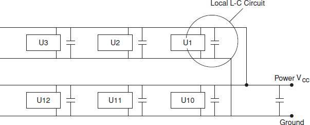
Software is available for EMI/EMC analysis.
National and international regulations exist to set standards for electromagnetic and power line emissions and associated test methods.
Most of the protection techniques against transient high voltages, described earlier, are useful in relation to EMI, and vice versa. Therefore the topics are often combined in specialist texts and training. Ott (2009) and Schmitt (2002) are good introductions to the whole field of EMI and EMC.
9.6.7 Redundancy
Redundancy techniques were covered in Chapter 6. In electronic circuit and system design it is possible to apply redundancy at any level from individual components to subsystems. Decisions on when and how to design-in redundancy depend upon the criticality of the system or function and must always be balanced against the need to minimize complexity and cost. However, it is often possible to provide worthwhile reliability improvements by using redundant circuit elements, at relatively little cost, owing to the low cost of most modern devices. The most likely component failure modes must be considered; for example, resistors in parallel will provide redundant, though possibly degraded operation if one becomes open circuit, and short circuit is an unlikely failure mode. Opposite considerations apply to capacitors.
9.6.8 Design Simplification
Like all good engineering, electronic system designs must be kept as simple as practicable. The motto often quoted is KISS – ‘Keep it simple, stupid’. In electronics, design simplification is mainly a matter of minimizing the number of components to perform a required function. Reducing the number of components and their connections should improve reliability as well as reduce production costs. However, the need to provide adequate circuit protection and component derating, and where necessary redundancy, should normally take priority over component count reduction.
Minimizing the number of component types is also an important aspect of design simplification. It is inevitable that when a number of designers contribute to a system, different solutions to similar design problems will be used, resulting in a larger number of component types and values being specified than is necessary. This leads to higher production costs, and higher costs of maintenance, since more part types must be bought and stocked. It can also reduce reliability, since quality control of bought-in parts is made more difficult if an unnecessarily large number of part types must be controlled.
Design rules can be written to assist in minimizing component types, by constraining designers to preferred standard approaches. Component type reduction should also be made an objective of design review, particularly of initial designs, before prototypes are made or drawings frozen for production.
9.6.9 Sneak Analysis
A sneak circuit is an unwanted connection in an electrical or electronic circuit, not caused by component failure, which leads to an undesirable circuit condition or which can inhibit a desired condition. Sneak circuits can be inadvertently designed into systems when interfaces are not fully specified or understood, or when designers make mistakes in the design of complex circuitry. Sneak analysis is a technique developed to identify such conditions in electrical and electronic circuits, and in operating software.
It is based on the identification within the system of ‘patterns’ which can lead to sneak conditions. The five basic patterns are shown in Figure 9.11.
Any circuit can be considered as being made of combinations of these patterns. Each pattern is analysed to detect if conditions could arise, either during normal operation or due to a fault in another part of the system, that will cause a sneak. For example, in the power dome or the combination dome the power sources could be reversed if S1 and S2 are closed.

Figure 9.11 Sneak analysis basic patterns (hardware).
Sneak circuits are of five types:
- Sneak paths. Current flows along an unexpected route.
- Sneak opens. Current does not flow along an expected route.
- Sneak timing. Current flows at the incorrect time or does not flow at the correct time.
- Sneak indications. False or ambiguous indications.
- Sneak labels. False, ambiguous or incomplete labels on controls or indicators.
When potential sneak conditions are identified, they must be validated by test or detailed investigation, reported and corrective action must be considered.
Sneak analysis is a tedious task when performed on relatively large systems. However, it has proved to be very beneficial in safety analysis and in assessing the integrity of controls in aircraft and industrial systems. Most of today's circuit simulation software packages have the capability of running sneak circuit analysis. Software applications are described in Chapter 10.
Sneak circuits can be avoided by careful design, or detected by adequate testing. The formal analysis technique is appropriate for critical systems, particularly when there are complex interfaces between sub-systems.
9.7 Parameter Variation and Tolerances
9.7.1 Introduction
All electrical parameters of electronic components are subject both to initial component-to-component variation, and sometimes to long-term drift. Parameter values can also vary as a result of other factors, particularly temperature. Whether these variations are important or not in a particular design depends upon the requirements for accuracy of the parameters in that application. For example, the resistance value of a resistor in a feedback circuit of a high gain amplifier might be critical for correct operation, but would not need to be as closely controlled in a resistor used as a current limiter.
Initial variation is an inevitable consequence of the component production processes. Most controlled parameters are measured at the end of production, and the components are assigned to tolerance bands, or rejected if they fall outside the limits. For example, typical resistors are provided in tolerance ranges of 1, 5, 10 and 20% about the nominal resistance. Since the selection is often from the same batch, which may have had a parameter distribution as shown in Figure 9.12, the parameter distributions of the selected tolerance ranges would be as shown, assuming only two tolerance bands had been selected. Depending upon the application, knowledge of the shape of the parameter distribution might be important.
For many component parameters, for example transistor characteristics, maximum and minimum values are stated. It is also important to note that not all parameter values are controlled in manufacture and selection. Some parameters are given only as ‘typical’ values. It is never a good idea to design critical circuit operation around such parameters, since they are not usually measured, and therefore are not guaranteed.
Since conductance, both of conductor and of semiconductor materials, varies with temperature, all associated parameters will also vary. Therefore resistance of resistors, and gain and switching time of transistors, are typical of temperature-dependent parameters. High temperature can also increase noise outputs. Other parameters can interact, for example the capacitance values between transistor connections is affected by bias voltage.
Parameter drift with age is also usually associated with changes in conductance, as well as in dielectric performance, so that resistors and capacitors are subject to drift, at rates which depend upon the type of materials and construction used, operating temperature and time.
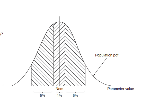
Figure 9.12 Parameter distributions after selection.
Another source of circuit parameter variation arises from what are referred to as parasitic parameters. These are electrical parameters that are not intrinsic to the theoretical design of the component or the circuit, but which are due to construction and layout features. For example, wire wound resistors are inductive, the inductance depending upon the type of construction, PCB conductor tracks have mutual inductance and capacitance, and integrated circuit lead frames are inductive. Parasitic effects can be very important, and difficult to control, in high gain and high frequency systems.
Parameter variation can affect circuits in two ways. For circuits which are required to be manufactured in quantity, a proportion might not meet the required operating specification, and production yield will then be less than 100%, adding to production cost. Variation can also cause circuits to fail to work correctly in service. Initial component-to-component variation mainly affects yield, and stress or time related variation mainly affects reliability.
9.7.2 Tolerance Design
Every electronic circuit design (for that matter, not only electronic circuits, but any system) must be based on the nominal parameter values of all the components that will contribute to correct performance. This is called parameter design. It encompasses the qualities of knowledge and inventiveness necessary for the solution of design problems. However, having created the correct functional design, it is necessary to evaluate the effects of parameter variation on yield, stability and reliability. This is called tolerance design.
The first step in tolerance design is to determine which parameter values are likely to be most sensitive in affecting yield and performance. This can be performed initially on the basis of experience and system calculations made during the parameter design stage. However, a more systematic approach, using the techniques described below, should be used for serious design.
The next step is to determine the extent of variation of all of the important parameter values, by reference to the detailed component specifications. This step is sometimes omitted by designers using lists of ‘preferred parts’, which list only primary nominal values and tolerances, without giving full details of other data relevant to the application. All relevant parasitic parameters should also be evaluated at this stage.
It is possible to design-in compensating features for some variation, for example by using temperature compensation components such as thermistors or adjustable components such as variable resistors. However, these add complexity and usually degrade reliability, since they are themselves prone to drift, and adjustable components can be degraded by wear, vibration and contamination. Wherever possible the design should aim for minimum performance variation by the careful selection of parameter values and tolerances.
9.7.3 Analysis Methods
The analysis of tolerance effects in general design situations will be covered in Chapter 11. This section introduces further methods available to analyse the effects of variation and tolerances in electronic circuits.
9.7.3.1 Worst Case Analysis
Worst case analysis (WCA) involves evaluating the circuit performance when the most important component parameter values are at their highest and lowest tolerance values. It is a straightforward extension of the parameter design calculations. However, it is only realistic for simple circuits. Also, purely digital circuits are relatively easy to analyse in this respect, so long as frequency and timing requirements are not too severe. However, if there are several parameters whose variation might be important, particularly if there are interactions or uncertainty, then more powerful methods of analysis should be used.
9.7.3.2 The Transpose Circuit
The sensitivity of the output of a circuit to parameter changes can be analysed using the transpose circuit method. A transpose circuit is a circuit which is topologically identical to that under investigation, except that the forward and reverse transmission coefficients of each 3-terminal device (e.g. transistor) are interchanged, the input is replaced by an open circuit, and the output by a current source of 1A. Figure 9.13 shows a circuit and a possible transpose of it. Here we are looking only at those components whose parameter variations we consider might most affect the output, in this case V0, when the input is Ii. Note that these are instantaneous values of terms in the frequency domain (or DC values).
The sensitivity of V0 to small changes in the conductance G of the resistor is given by
![]()
where VG is the voltage across the conductance in the actual circuit and VG/T is the voltage across the conductance in the transpose circuit. Similar relations hold for other component parameters, if the two circuits are analysed at the same frequency. This is Tellegen's theorem. Using these relationships, the sensitivities to all the critical parameters can be evaluated, by analysing only two different circuits, using for example circuit simulation software. This is an extremely efficient technique for analysing the effects of small, single variations. It is described in Spence and Soin (1988).
9.7.3.3 Simulation
Another method for analysing the effects of tolerances and variation is simulation, using the Monte Carlo method. The principles of Monte Carlo simulation were described in Chapter 4. Most modern circuit simulation software packages include Monte Carlo techniques, which allow parameter variations to be set, either as a range or as a defined distribution shape (e.g. normal, bimodal), and the program will then randomly ‘build’ circuits using parameter values from the distributions, and will analyse these. Monte Carlo circuit simulation evaluates the effects of multiple simultaneous variations. Refinements allow the most critical parameters to be identified, and statistically designed experiments (see Chapter 11) can be run. Circuits can be analysed in the time and frequency domains, and there are no practical limitations, apart from the time required to run each analysis, on the number of parameters, input conditions and simulations.

Figure 9.13 Transpose circuit (from Spence and Soin (1988)).
Figure 9.14 shows the results of a number of Monte Carlo simulations of a filter circuit, in relation to the specification. This shows that some parameter combinations give performance outside the specification. Carrying out a number of runs provides an estimate of production yield, and the particular parameter value combinations that caused circuits to be outside the specification can be identified.
See Singhal and Vlach (2010) and Spence and Soin (1988) for descriptions of the topics covered in this section.

Figure 9.14 Monte Carlo analysis of filter circuit (from Spence and Soin (1988)).
9.8 Design for Production, Test and Maintenance
Electronic circuits should be designed to be testable, using the test methods that will be applied in production. These methods depend upon the manufacturing test policy and economics, as discussed in Chapter 15. Testability is an important design feature, which can make a significant impact on production costs. Testability also affects reliability, since production defects which are not detected by the tests can lead to failure in service, and circuits which are difficult to diagnose are more likely to be inadequately or incorrectly repaired.
It is important that the circuit designer is aware of the test methods that will be used, and the requirements that they impose on the design to ensure effective and economic test coverage. Test methods for electronics are described in O’Connor (2001).
Circuit designs must allow the ATE to initialize the operating states of components, control the circuit operation, observe and measure output states and values, and partition the circuit to reduce test program complexity. It is good practice to conduct a careful review, with the test engineers, of the testability of the design before it is finalized. Modern EDA software includes facilities for performing testability analysis. Turino and Binnendyk (1991) cover the subject of design for test in detail.
Design of electronic systems for production, test and maintainability should be included in design rules and design review. Aspects of good electronic design which contribute to these are listed below:
- Avoid the necessity for adjustments, for example, potentiometers, whenever possible. Adjustable components are less reliable than fixed-valued components and are more subject to drift.
- Avoid ‘select on test’ situations, where components must be selected on the basis of measured parameter values. Specify components which can be used anywhere within the tolerance range of the applicable parameters and do not rely on parameters which are listed as typical rather than guaranteed. Where ‘typical’ tolerances must be used, ensure that the appropriate component screening is performed before assembly.
- Ensure that adjustments are easily accessible at the appropriate assembly level.
- Partition circuits so that subassemblies can be tested and diagnosed separately. For example, if several measured values require amplification, analogue-to-digital conversion, logic treatment and drivers for displays, it might be better to include all functions for each measured value on one PCB rather than use a PCB for each function, since fault diagnosis is made easier and repair of one channel does not affect the performance or calibration of others. However, other factors such as cost and space must also be considered.
Questions
- How does increasing temperature affect the reliability of electronic components? Illustrate your answer with three examples of specific failure mechanisms and component types.
- Briefly describe three failure modes that can occur in modern integrated circuits. In each case, explain how they are influenced by temperature (high/low), electrical stresses, and manufacturing quality.
- Describe the design, manufacturing and application factors that influence the following failure modes of integrated circuits: (i) electromigration; (ii) latch-up; (iii) electrostatic damage.
- Screening is a process used to improve the quality and reliability of integrated circuits. Explain the engineering justification for IC screening, and describe briefly the tests that are typically applied in the screening process.
- How have the recent developments in microcircuit device packaging affected reliability? How can the risks of failure be minimized?
- What are the main factors to consider, from the reliability point of view, when selecting the type of packaging for the integrated circuits to be used in a circuit designed for mass production? Consider hermetic versus plastic packaging, and through-hole versus surface mounting.
- Suggest ways in which the capability approval process is a more useful approach to ASIC line approval than the approved components system.
- Use the equation from MIL-HDBK-217 from Chapter 6 λp = πQπL[C1πT + C2πE]/106h to calculate the device hazard rate for a device screened to level B-1 (πQ = 2.0) from the following data: πL = 1, C1 = 0.12, πT = 3.7, πV = 1, C2 = 0.01, πE = 4.2. What is the use of the hazard rate calculated in this way?
- Discuss the reliability of electronic components as an overall contributor to system reliability in modern systems.
- Describe the ways in which solder connections can fail. How can circuit designers minimize solder failures?
- Describe the ways in which electrical cables and connectors can fail. How can circuit designers minimize these failures?
- What are ‘no fault found’ failures? Describe the main causes of such failures. Why are they important?
- Why are the thermal aspects of electronic system design important for reliability? What methods can designers use to reduce the operating temperatures of electronic components?
- A supplier has presented you with a derating policy based on deriving the derating curves from power stress versus base hazard rate curves from MIL-HDBK-217 data. State your reservations concerning this approach.
-
- for a small plastic transistor operating at 120 mW, estimate TJ if θ = 0.4°C mW−1 above 25 °C, if the ambient temperature is 50 °C.
- If the maximum junction temperature is 150 °C, estimate what power the transistor will dissipate at an ambient temperature of 60 °C.
- Using Figure 9.9 and Table 9.3, estimate the percentage power allowed for a general-purpose silicon plastic-sealed transistor in a Hi-rel application.
- State some of the advantages of employing thermal derating techniques in an electronic design.
- What are the main sources of electromagnetic interference (EMI) that can affect electronic systems? Describe three methods that can be used to protect circuits from EMI.
- In a normal domestic kitchen containing a fluorescent light fitting and a washing machine, list the EMI sources you may find and how as a designer you may mitigate these effects.
- Describe three methods for analysing the effects of component parameter variations on the performance of an electronic circuit. For each, describe how the variations and their effects can be minimized by the designer.
- Discuss and compare reliability characteristics of tin-lead vs. lead free solder. Describe pros and cons of the transition to lead-free solder. Make examples of where you would prefer tin-lead and where you would prefer lead-free solder.
- You conducted a series of experiments with electromigration at two different temperatures T1 = 25 °C and T2 = 60 °C. The current density in the first case was 2mA/μm2 and in the second 1mA/μm2; the activation energy is EA = 0.6 eV. As a result of the experiments MTTF1 = 1457 hours and MTTF2 = 500 hours. Determine both experimental constants A and N in Black's equation (9.1).
- A resistor is advertised as being rated at 2 Watt. You have a choice of using this resistor in a 1 Watt application and in a 3 Watt application. Which case would constitute derating and which is uprating? Explain your answer.
Bibliography
General
CALCE (2011) Lead Free and Green Electronics Forum, CALCE, University of Maryland. Available at: http://www.calce.umd.edu/lead-free/index.html.
Clech, J-P. (2004) Lead-Free and Mixed Assembly Solder Joint Reliability Trends. Proceedings (CD-ROM), IPC / SMEMA Council APEX 2004 Conference, Anaheim, CA, Feb. 23-26, 2004, pp. S28-3-1 through S28-3-14. Available at http://www.jpclech.com/EPSI_Publications.html.
Clech, J-P., Henshall, G. and Miremadi, J. (2009) Closed-Form, Strain-Energy Based Acceleration Factors for Thermal Cycling of Lead-Free Assemblies, Proceedings of SMTA International Conference (SMTAI 2009), Oct. 4-8, 2009, San Diego, CA.
DfR Solutions (2010) Pb-Free Solder Joints. Available at http://www.dfrsolutions.com/pb-free-solder-joints/.
Evans, J. (2010) A Guide to Lead-free Solders. Physical Metallurgy and Reliability (ed. W. Engelmaier), Springer.
Garrou, P. and Gedney, R. (2004) Tin Whiskers: An Industry Perspective. Advanced Packaging, December 2004 issue.
Horowitz P. and Hill, W. (1989) The Art of Electronics, 2nd edn, Cambridge University Press.
JEDEC (2006) JESD201 standard, Environmental Acceptance Requirements for Tin Whisker Susceptibility of Tin and Tin Alloy Surface Finishes. Available at http://www.jedec.org/standards-documents.
Pascoe, N. (2011) Reliability Technology: Principles and Practice of Failure Prevention in Electronic Systems, Wiley.
Pecht, M. (ed.) (1995) Product Reliability, Maintainability and Supportability Handbook. ARINC Research Corp.
US MIL-HDBK-338. Electronic Reliability Design Handbook. Available from the National Technical Information Service, Springfield, Virginia.
Components
Amerasekera, E. and Najm, F. (1997) Failure Mechanisms in Semiconductor Devices, 2nd edn, Wiley.
Bajenescu, T. and Bazu, M. (2011) Failure Analysis: A Practical Guide for Manufacturers of Electronic Components and Systems, J. Wiley.
Brindley, K. and Judd, M. (1999) Soldering in Electronics Assembly, Newnes.
Bajenescu, T. and Bazu, M. (1999) Reliability of Electronic Components, Springer-Verlag.
British Standard, BS 9000. Components of Assessed Quality. British Standards Institution, London. (And equivalent US MIL, European (CECC) and International (IEC) standards.)
Das, D., Pendse, N., Wilkinson, C. and Pecht, M. (2001) Parameter Recharacterization: A Method of Thermal Uprating. IEEE Transactions on Components and Packaging Technologies, 24(4), December 2001
Hannemann, R., Kraus, A. and Pecht, M. (1997) Semiconductor Packaging: A Multidisciplinary Approach, Wiley.
Harper, C. (2004) Electronic Packaging and Interconnection Handbook, 4th edn, McGraw-Hill Professional.
IEC TR 62240 (2005) Process management for avionics –Use of semiconductor devices outside manufacturers' specified temperature range.
Jensen, F. (1995) Electronic Component Reliability, Wiley.
Kleyner, A. and Boyle, J. (2003) Reliability Prediction of Substitute Parts Based on Component Temperature Rating and Limited Accelerated Test Data. Proceedings of Annual Reliability and Maintainability Symposium, Tampa, Florida, pp. 518–522.
Kuo, W., Chien, W. and Kim, T. (1998) Reliability, Yield, and Stress Burn-In: a Unified Approach for Microelectronics Systems Manufacturing & Software Development, Springer.
Lau, J., Wong, C., Prince J. and Nakayama, W. (1998) Electronic Packaging: Design, Materials, Process, and Reliability, McGraw-Hill.
Ohring, M. (1998) Reliability and Failure of Electronic Materials and Devices, Academic Press.
Pecht, M. (ed.) (1993) Soldering Processes and Equipment, Wiley.
Pecht, J. and Pecht, M. (eds) (1995) Long-Term Non-Operating Reliability of Electronic Products, CRC Press.
Pecht, M., Radojcic, R. and Rao, G. (1999) Guidebook for Managing Silicon Chip Reliability, CRC Press.
Tummala, R. (2001) Fundamentals of Microsystems Packaging, McGraw-Hill.
Tummala, R., Rymaszewski, E. and Klopfenstein, A. (1997) Microelectronics Packaging Handbook, Kluwer Academic Publishers.
US MIL-STD-883. Test Methods and Procedures for Microelectronic Devices. Available from the National Technical Information Service, Springfield, Virginia.
Woodgate, R. (1996) The Handbook of Machine Soldering: SMT and TH, 3rd edn, Wiley-Interscience.
Mechanical and thermal effects and design
Lall, P., Pecht, M. and Hakim, E. (1997) Influence of Temperature on Microelectronics and System Reliability, CRC Press.
McCluskey, P., Grzybowski R. and Podlesak, T. (eds) (1997) High Temperature Electronics, CRC Press.
Sergent, J. and Krum, A. (1998) Thermal Management Handbook: For Electronic Assemblies, McGraw-Hill.
Steinberg, D. (2000) Vibration Analysis for Electronic Equipment, 3rd edn, Wiley.
Thermal Guide for Reliability Engineers. Rome Air Development Center Report TR-82-172. Available from the National Technical Information Service, Springfield, Virginia.
EMI/EMC/ESD
Chatterton, P. and Houlden, M. (1991) EMC: Electromagnetic Theory to Practical Design, Wiley.
Ott, H. (2009) Electromagnetic Compatibility Engineering, Wiley-Interscience.
Schmitt, R. (2002), Electromagnetics Explained: A Handbook for Wireless/RF, EMC, and High-Speed Electronics. Elsevier.
US MIL-E-6051D, Electromagnetic Compatibility Requirements, Systems. NTIS, Springfield, VI.
US MIL-STD-461D, Requirements for the Control of Electromagnetic Interference Emisions and Susceptibility. NTIS, Springfield VI.
Tolerance design and electronics testing
O'Connor, P.D.T. (2001) Test Engineering. Wiley.
Singhal, K. and Vlach, J. (2010) Computer Methods for Circuit Analysis and Design, Kluwer Academic Publishers.
Spence, R. and Soin, R. (1988) Tolerance Design in Electronic Circuits, Addison-Wesley.
Turino, J. and Binnendyk, H. (1991) Design to Test, 2nd edn, Logical Solutions Inc., Campbell, CA (Also Testability Advisor software).