
Day 7 Running
The Plan
In the six previous days of exploration, we have gradually begun reviewing the most basic concepts of C programming as they apply to embedded control and in particular as they apply to the PIC32MX architecture. We have also started to familiarize ourselves with the basic features of the PIC32 that affect its performance, such as the 32-bit multiplier, the interrupt system, the register set(s), and the memory management module. But so far, we have only been counting the number of assembly instructions looking inside the disassembly window, or counting the instruction cycles, using the MPLAB® SIM simulator StopWatch. In all cases we avoided any direct reference to time when considering the execution of code, using peripherals (timers) when necessary to provide delays of any length. Even when discussing interrupts or comparing the efficiency of various numeric types, we have not yet established any hard relationship with the actual speed of execution of our code. This was done on purpose, to isolate different subjects and keep the level of complexity growing gradually. Before we can understand how fast we can make a PIC32 truly “run,” we need to study two new critical systems: the clock system and the memory cache system. Both are new to the PIC® architecture and are essential if you want to fine-tune the PIC32 engine for maximum performance.
Preparation
Today, in addition to the usual software tools, including the MPLAB IDE and the MPLAB C32 compiler, you will need real hardware to be able to perform our experiments. It does not matter if you have a PIC32 Starter Kit or any of the other in-circuit debuggers connected to an Explorer 16 demonstration board. You will need the real thing—a PIC32MX chip “running” on the hardware platform of your choice.
Use the New Project Setup checklist to create a new project called Running and a new source file, similarly called running.c.
The Exploration
Let’s start by taking a look at the main clock circuit of the PIC32MX family. As you can see from the block diagram in Figure 7.1, this is a complex piece of hardware with which it will require some time to become familiar.
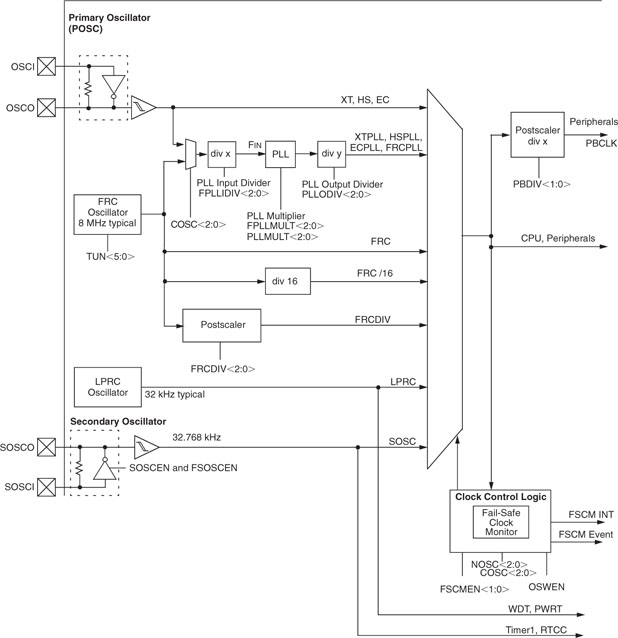
For those of you already knowledgeable about the previous generations of 8-bit PIC microcontrollers, most of this diagram will look somewhat familiar. For those of you familiar with the dsPIC33 and PIC24 H families in particular, it will look exceptionally similar! This is of course no coincidence. All PIC microcontrollers, since the very first PIC16C54, have sported a flexible oscillator circuit, and this flexibility has been extended generation after generation, evolving gradually into the present form as offered on the PIC32MX. Let’s see what can be done, and most importantly, why!
Looking at the left side of the block diagram, you will notice that there are five oscillators or clock sources. Two of them use internal oscillators and three of them require external crystals or oscillator circuits:
These five sources offer a basic range of choices to generate an input clock signal of desired frequency, power consumption, and accuracy, but much more can be done with the following stages, illustrated on the right side of the block diagram. In fact, the clock produced by each source can be further multiplied and/or divided to offer an even wider selection of frequencies.
Performance vs. Power Consumption
It is beyond the scope of this book to illustrate all possible options for each clock source, but it is important that you understand the reason why the designers of the PIC32 went through all this effort to offer you so many different ways to produce what is, after all, a simple square wave.
In embedded control, but also in consumer applications, whether your application is portable—battery powered—or has a dedicated power supply of sorts, two important constraints apply:
As is often the case, in embedded-control application design, the two constraints are in direct conflict. To obtain a greater amount of work from a given circuit, we want to maximize the clock speed. But because of the laws of physics that govern the operation of any CMOS integrated circuit, the higher the clock speed provided, the higher is the power consumption of the device. The two entities are in fact linked inexorably in a linear relationship: Double the clock and you will double the amount of work produced, but you will also see a corresponding increase in the power consumption of the device.
Note
The power consumption will not double as you double the frequency. There is a static component and a dynamic component to the power consumption of each CMOS device. The first one remains constant independent from the clock frequency; it is only the dynamic part that will grow.
Much can and has been done inside the PIC32 to make sure that the greatest amount of work is produced for any given ounce of power. For example, the PIC32MX datasheet (only the advanced datasheet is available at the time of this writing) reports on the electrical characteristics of the device that, when operating at the frequency of 4 MHz, a typical current consumption of 11 mA will be observed (at 3.3 V and 25°C). But at 72 MHz and in the same conditions, the same device will consume just 64 mA.
As good as these numbers are, it is still our responsibility to find the correct balance between performance and power consumption for each application so to minimize cost, reduce size, or simply maximize the battery life (and, let me add, “fight global warming as well”!).
Not only does it make no sense to run an applications at 72 MHz when the same job can be done at 4 MHz, but also consider the fact that most applications operate in different modes at different times. Although it might seem overkill, I will make a parallel with a cell phone application. Most of the time, the cell phone is in standby just waiting for a button to be pressed to awake it. At other times it could be performing simple functions such as searching through a contact book and updating information on the internal memory. Then only a small fraction of the time will be spent performing some hard number crunching, digital signal processing, and running an algorithm to compress and decompress the audio input and output streams.
Similar conditions can be found in many embedded-control (and consumer) applications, and the higher the flexibility of the clock circuit, the better you will be able to manage the power consumption of the application. To help you obtain the most complete set of power management options, the PIC32 clock module offers the following features:
The Primary Oscillator Clock Chain
We will begin our exploration at the primary oscillator clock signal chain, since it is the most common and, in many of the following chapters, we will need to develop demonstration projects that will require either a high level of performance or high clock accuracy. As you can verify visually, on the Explorer 16 demonstration board and PIC32 Starter Kit, an 8 MHz crystal is connected across the OSCI and OSCO pins. At this frequency (below 10 MHz) it is recommended we set the primary oscillator for operation in XT mode.
Depending on the application, we are immediately confronted with two possibilities. We could use the 8 MHz input signal as is or feed it to a multiplier (PLL) circuit. The appeal of the second option is obvious, but with it comes the need to learn more about PLL circuits.
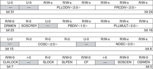
Phase locked loops (PLLs) are complex little circuits, but the designers have managed to hide all the complexity of the PIC32 PLL from us with the condition that we respect a few simple rules. First, we need to feed it with a specific input frequency range (<4 MHz). Second, we need to allow it time to stabilize or “lock” before we attempt to execute code and synchronize with it. A simple control mechanism is provided (via the OSCCON register illustrated in Figure 7.2) to select the frequency multiplication factor (PLLMULT) and to verify the proper locking (SLOCK).
So when using the Explorer 16 board or the PIC32 Starter Kit, to respect the first rule we will need to reduce the input frequency from 8 MHz to 4 MHz. Looking at the block diagram in Figure 7.1 or the simplified diagram in Figure 7.3, you will notice how the input divider is conveniently available to us to perform the first frequency reduction.
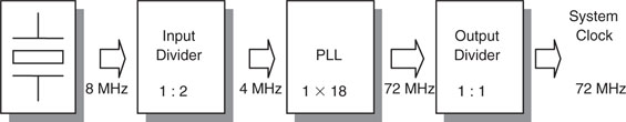
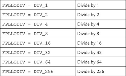
The multiplication factor of the PLL can be selected among a number of values ranging from 15× all the way up to 24× and it is controlled by the PLLMULT bits. Since the maximum operating frequency of the PIC32MX is (at the time of this writing) restricted to 75 MHz, selecting a factor of 18× will give 72 MHz, the closest match compatible with the device operating specifications. The output divider block provides us with a final opportunity to manage the clock frequency. When we will need the maximum performance, we will leave the output divider set to a 1:1 ratio. Should our application require it, we will be able to reduce the power consumption by dividing the output frequency all the way down to 1:256th or approximately 280 kHz. Below this frequency we would be much better served by using the secondary oscillator (SOSC), its operating range is in fact between 32 kHz and 100 kHz, or by the low power internal oscillator (LPRC) operating at approximately 32 kHz. For our reference, from the advanced datasheet we learn that the typical power consumption of the PIC32 when operating off the LPRC would be just 200 μΑ!
The Peripheral Bus Clock
As another way to optimize performance and power consumption in an application, the PIC32 feeds a separate clock signal to all the peripherals. This is obtained by sending the System clock through yet another divide circuit (extending further the chain of modules illustrated in Figure 7.3), producing the PB clock signal. Very often a high processor speed means that a large prescaler is required in front of a timer to obtain the required timing, or a large baud rate divider is required for a serial port (more on this later). Thanks to the peripheral bus divider, the share of power consumed by the peripheral bus can be reduced while the processor is free to operate at maximum speed.
This feature is controlled by the PBDIV bits found, once more, inside the OSCCON register. A reasonable value that we have been using so far and we will continue to use consistently for the peripheral bus across all future example projects will be 36 MHz corresponding to 1:2 ratio between the system clock and the PB clock.
Initial Device Configuration
The ability to control the clock at run time gives us a great tool to manage power, but what happens when the device is first activated, at power-up?
As you might know, there is a group of bits known as the configuration bits stored in the nonvolatile (Flash) memory of the PIC32. These bits provide the initial configuration of the device. The oscillator module uses a few of those bits to get the initial setting for the OSCCON register. These are the configuration bits you can set using the MPLAB Configure | Configuration Bits … menu.
It is about time that we review the settings I have been recommending that you use since the beginning using the Device Configuration checklist.
My recommended configuration for all the exercises in this book is represented in Figure 7.4. It includes the following options, in order of importance for the oscillator configuration:
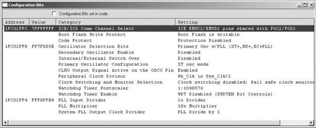
The following additional options complete the configuration:
Finally, the following options are commonly used during debugging and development:
Once set, these configuration bits are stored in the workspace file (.mcw) and will be programmed into the device configuration bits by your programming tool of choice each time new code is programmed into the device.
By comparing Figures 7.2 and 7.4, you will notice that the value of the PLL input divider is present only as a configuration bit option, but it cannot be modified via the OSCCON register. If you reflect on this, you will find it is logical. Since the external crystal value cannot change (unless the part is unsoldered from the PCB and a new one of different frequency is put in its place), there is no possible reason to modify the input divider value at run time. If the value set by the configuration bits was incorrect in the first place, the PLL multiplier would not be working and the PIC32 could not execute any code anyway.
Setting Configuration Bits in Code
As a way to make the project code self-documenting and to avoid any possible future mishap (should the project file be lost and the source code of an application used with the wrong settings), the MPLAB C32 compiler offers one additional mechanism to assign values to the device configuration bits. It is based on the use of the #pragma config directive.
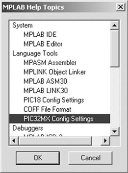
Since the number of configuration bits and their values can change from device to device, MPLAB offers a list of the available options for each PIC32 device model as part of the Help system. Select Help | Topic to open the help system selection dialog box, and click PIC32MX Config Settings (see Figure 7.5).
Select the device model that you are using, PIC32MX360F512L, and then identify the correct syntax to be used for each configuration bit. Table 7.1 shows the PLL output divider example.
Multiple configuration bits can be set inside a #pragma config statement by separating them with a comma, as in the following example, where I have reproduced the standard oscillator settings as described previously:
![]()
Notice that if a parameter is not specified in the #pragma, it will assume the default value as specified in the device datasheet.
Let’s complete the configuration with one more #pragma statement to set the peripheral bus clock divider, disable the watchdog and the code protection, and to enable programming of the boot memory as required for all our future projects (at least during the development phase):
![]()
My recommendation is that you place this code at the top of the source file containing the main function in each new project.
To avoid conflicts with the configuration bits set by MPLAB in the Configuration Bits dialog box (refer back to Figure 7.4), make sure to check the Configuration Bits Set in Code check box.
Note
When the Configuration Bits Set in Code check box is checked, the entire contents of the dialog box are grayed out. This is the default for every new project. Be careful, though—if you forget to set the #pragma config statement in your code, you’ll end up with the default device configuration, as described in the device datasheet. This default configuration is designed for “safe” operation and most of its settings are conflicting or incorrect for use during development. I chose not to set the configuration bit in code in the first few chapters of the book to avoid the “distraction” in your code and to avoid having to anticipate too much too soon. From now on, the choice is yours!
Heavy Stuff
It is time to write some tough code, program it on a PIC32 Starter Kit or an Explorer 16 demonstration board, and start measuring the actual performance of the PIC32MX.
See what I found in my code archives! Buried in a remote subdirectory of my hard drive, back from the old days at university when I studied the basics of digital signal processing, I wrote this code:
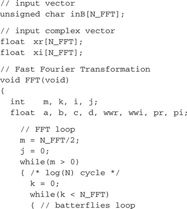
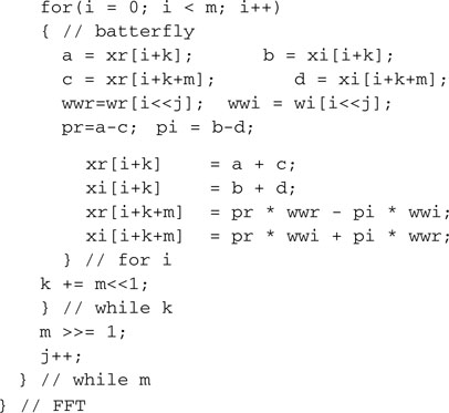
This is the Fast Fourier Transform (FFT) function, one of the most common digital signal processing tools, albeit in a simplified form designed to operate on a set of samples whose size is purposely chosen as a power of two. The FFT is an efficient algorithm to compute the discrete Fourier transform (DFT) and its inverse, that is, what takes us from a signal time domain representation to the same signal in the frequency domain representation and back. In other words, if you supply as input to an FFT function an array of values (inB[] ) that represent samples of an input signal, the function will return a new array containing values corresponding to the amplitudes of each harmonic (sinusoidal component) of the input signal—i.e., the signal frequency spectrum. FFTs are of great importance to a wide variety of applications beyond digital signal processing, including solving partial differential equations and algorithms for quick multiplication of very large integers. Many studies have been done on how to optimize FFTs and determine the minimum possible number of arithmetic operations required to perform them on a given data set. But we are not interested in optimizing the algorithm here; on the contrary, we will use the “scholastic” implementation as an example of an algorithm requiring heavy floating-point arithmetic for our performance-testing purposes.
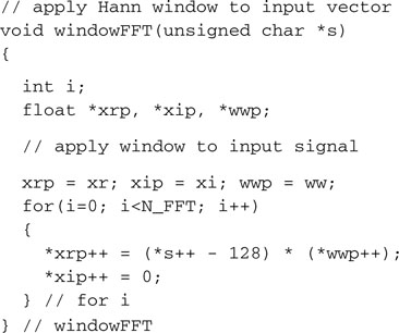
Actually, the algorithm illustrated previously represents only a part of the work that a complete discrete Fourier transform implementation requires. To obtain the necessary accuracy, the input data set must first be windowed before use. Think of it as though a segment of the input signal was cut abruptly and its sharp edges at the extremities need to be filed to smooth out the algorithm response:
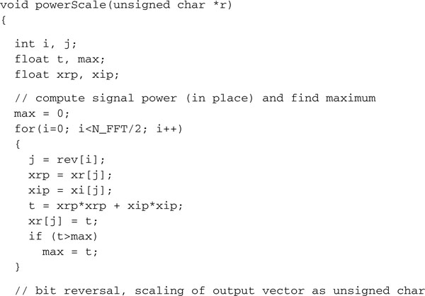
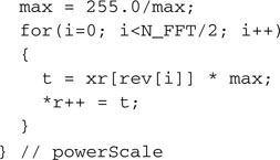
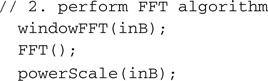
After the FFT, the modulus of the (complex) output must be taken and scaled back in place, in this case overwriting the input array:
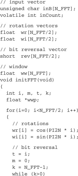
To streamline operation and avoid obvious inefficiencies, a minimum of housekeeping is typically performed ahead of time by initializing a few arrays containing frequently used values such as the so-called rotations array, the window array itself, and the bit reversal array. Here is how we define them and the initialization function we can use:
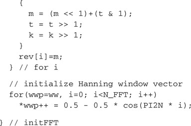
Scared? Confused? Don’t be! Take this code as is; it’s heavy stuff. The larger N_FFT, the number of samples in your input array, the harder it gets for our PIC32 to work on it.
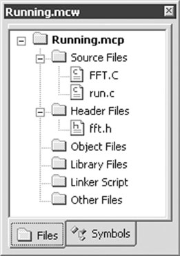
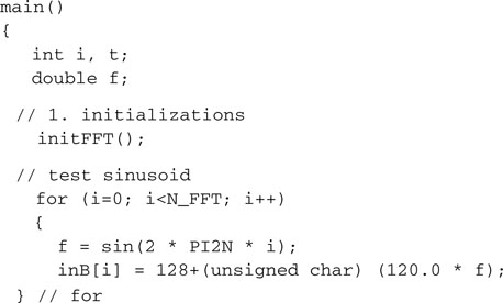
All we need to do, for now, is to package it nicely in a source file, save it as fft.c, and then add it to the source files of a new project that we will call Running.
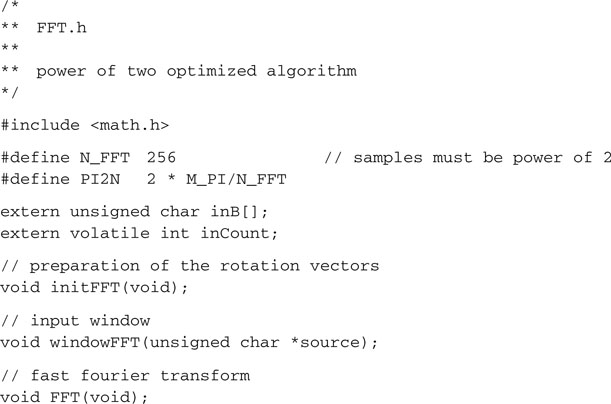
To keep things clean and tidy, let’s also prepare a small include file fft.h where we will define all the symbols required to use the fft.c module.
![]()
Add fft.h to the include files of the Running project as well.
Next let’s create our project main source file. How about run.c for a name (see Figure 7.6 )?
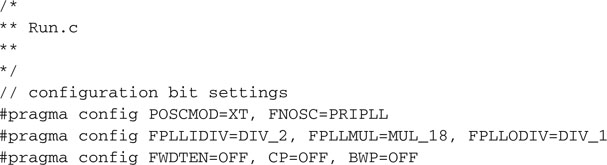
Let’s add the configuration bit settings at the very top of the source code for maximum visibility, and let’s include the fft.h file as well since we will soon use all its functions:

Now let’s create a main function that, in order, will perform the following:
Ready, Set, Go!
At this point we could already build the project, program a device, and, using a couple of breakpoints and a manual stopwatch, we could try to capture the actual time required. But the effort would be extremely tedious and imprecise. I have a better idea: Why don’t we make the PIC32 time itself?
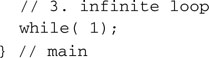
We can use, once more, one of the five 16-bit timers available or, for the occasion, we could experiment using for the first time a “pair” of timer modules combined to form a 32-bit timer. This option is available for the pairs formed by Timer2 and Timer3 together as well as Timer4 and Timer5. The latter pair is used in the following example, to bracket the FFT sequence:
Notice how I used the functions from the timer.h library, and including plib.h at the top of the program, we automatically included all the peripheral libraries at once.
The OpenTimerXX() function allows us to configure the timer, selecting the clock source and the prescaler value. It is equivalent to writing directly to the TXCON register as we did in the previous explorations, if only slightly more readable. The main drawback, as often is the case for these peripheral libraries, is that you won’t find the list of valid parameters to use (such as T4_SOURCE_INT) inside the device datasheet where the timer module is described; you will have to rely instead on a separate document (the library manual) and often resort to inspecting personally the include file—timer.h in this case. It is in fact by inspecting this file (you can open it with the MPLAB Editor) that you will learn how, when used as a pair, the correct parameters to pass to the initialization function are taken from those of the first module of the pair (T4 in our case).
The function WriteTimerXX(), as you would expect, allows us to set the initial counter value and effectively start our stopwatch, while the function ReadTimerXX() will read a 32-bit count value. It won’t stop our stopwatch, but it will take a reading at that precise moment; that is what we need.
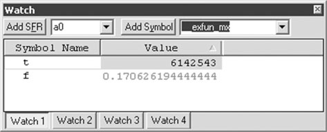
Let’s open the Watch window by selecting the View | Watch menu and Add the symbol t to it. Unless you have already configured the Watch window to use decimal as the default format, click with the right mouse button on top of the symbol t to activate the Watch window context menu, and choose Properties. Select Decimal as the default representation for this variable.
Now you are ready to build our project and program it onto the device with your development tool of choice. Set a breakpoint on the line containing the infinite loop, press Run, and sit back and relax while the PIC32 works hard to solve the problem for you. After a short while, MPLAB will come back alive as the PIC32 reaches the breakpoint, and we will be able to read the timed value from the 32-bit integer variable t. In my case it turned out to be 6,140,495!
Well, at least now you understand why I suggested we use a 32-bit timer. As fast as a fast Fourier transform can be, it is hard work, and a 16-bit timer would not suffice to keep track of such a large number of cycles.
Converting the timer count in actual seconds, milliseconds, and microseconds is not hard if we remember how we configured the oscillator and the primary clock path. The PIC32 system bus clock frequency was set to 72 MHz, while all the peripherals were provided a 36 MHz peripheral bus clock. Dividing the timer value by the peripheral bus frequency, we obtain:
T = t/Fpb = 6,142,543/36,000,000 = 0.17062 s
We can automate the conversion by asking the PIC32 to do it for us from now on—just add the following line of code after the stopwatch capture:
f = t/36E6;
This will reuse the variable f to perform the division using floating-point arithmetic. Add f to the Watch window so that, from now on, we will get to see the result of our experiments expressed correctly in seconds and fractions (see Figure 7.7).
Fine-Tuning the PIC32: Configuring Flash Wait States
Whether you think that 170 ms is a good time in which to perform a 256-point FFT or not, of one thing I am sure: The PIC32 can do better. In fact, beyond selecting the fastest clock speed and properly configuring the oscillator module, a number of advanced mechanisms on the PIC32 still require our attention to achieve the fine tuning that will provide us with the highest possible level of performance. The number-one limitation to the performance of an embedded control processor is the speed of its Flash memory. Unfortunately, once more, there is a conflict of interest; the fastest available Flash memory banks are also the ones requiring the highest power consumption.
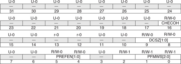
The designers of the PIC32 found that a perfect balance could be obtained by using a low-power Flash memory and decoupling the PIC32 core system bus from the memory bus by providing the ability to add a number of wait states (corresponding to up to seven clock cycles), during which the processor is stalled waiting for data to be fetched from the Flash memory. Depending on the difference in speed between memory and core, an increasing number of wait states might be required. By default, at power-up this mechanism is set for the safest possible condition that is reached by setting the maximum number of wait states. Hence there is an opportunity for us to reduce the number to the minimal possible value, given the actual operating specifications of the device. The number of wait states is controlled by the CHECON special function register (see Figure 7.8) and in particular by the PFMWS bits.
We could directly assign values, between 0 and 7, to the CHECON register’s bits, as in the following example:
![]()
But we would have to assume the responsibility for identifying the minimum safe number of wait states for the worst-case operating conditions of our application (relying on the electrical characteristics from the device datasheet). In fact, should we use the wrong number of wait states, the execution of code from Flash memory could become erratic, and to make things worse, this would become detectable only under specific extreme conditions of power supply voltage and temperature.
As a better alternative, we can use an ad hoc library function provided with the PIC32MX peripheral libraries: SYSTEMConfigWaitstatesAndPB(freq). The function requires the system clock frequency to be passed as an integer parameter and was designed by the PIC32 application support team to set the “recommended” minimum wait states for the given system clock frequency, taking all the guesswork away.
Note
The … AndPB part of the function name is supposed to remind us that the same function will also automatically modify the peripheral clock frequency setting of the PB divider as required to keep the peripheral bus always below 50 MHz. As it happens, this is exactly what we had the system configured for (at power-up) anyway.
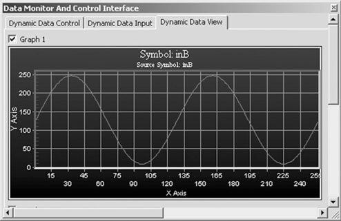
So it is time to give a second try at our project, with the added “tuning” of the wait states performed by the following line of code (placed inside the initialization section of our main() function):
![]()
Rebuild the Running project and reprogram your development board. Let the application run once more until it reaches the breakpoint (see Figure 7.9).
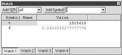
Now, this is an improvement! We just reduced the FFT execution time from 170 ms to 42 ms. This is better than a 4× speed improvement.
Fine-Tuning the PIC32: Enabling the Instruction and Data Cache
But there is so much more we can do. As we understand more of the PIC32 architecture, we notice that between the MIPS core bus and the memory bus there is actually an entirely new module: the cache. Think of it as a small but very fast block of RAM memory sitting between the processor and the Flash memory. Every time the processor fetches an instruction or a word of data from the Flash memory, the cache module will keep a copy but will also remember the address. When and if the processor needs the same data again (from the same address) in the (near) future, the cache will quickly be able to retrieve it, avoiding any new access to the Flash memory block (and avoiding all wait states eventually associated).
The larger a cache memory module, the higher the probability that a copy of a specific piece of data or instruction will be found in it. The reverse is also true: The shorter the inner loop of a given algorithm, the higher the impact that the availability of the cache module will have on its performance. This is because once all the cache is filled and a new instruction is fetched, the content of the cache must be “rotated,” and the oldest or least recently used instruction/data needs to be overwritten by the new information.
Unfortunately, cache memory is, by its very nature, very expensive, and the PIC32MX designers had to balance costs and benefits by setting the maximum capacity of 16 lines of 16 bytes each, for a total of 64 complete 32-bit instructions, equivalent to 256 bytes.
There is much more flexibility (and therefore complexity) involved in the inner workings of the PIC32 cache module, but we don’t need to know much more for now to decide that we like the cache module and we want to activate it. In fact, by default at power-on, it is disabled, and as in the previous case, there is a convenient library function (defined in the pcache.h module) awaiting our call:
![]()
Note
The Kseg0 is the virtual memory space where MPLAB C32 allocates all the code segments produced by compiling our project codes by default. You will remember that code placed in this address space “can” be cached, whereas code place in Kseg1 will not be cached, regardless of the cache module settings and status.
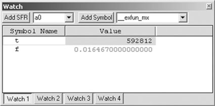
Rebuild the Running project and reprogram your development board. Let the application run once more until it reaches the breakpoint (see Figure 7.10).

Now, this is another important improvement! We just reduced the FFT execution time from 42 ms to 20 ms. This is a further 2× speed improvement.
Fine-Tuning the PIC32: Enabling the Instruction Pre-Fetch
But we are far from finished. The cache module of the PIC32 has another important feature to offer that promises similarly large rewards once enabled. It is the ability to perform instructions pre-fetching. That is, the cache module not only records the instructions being fetched by the PIC32 core; it also “runs ahead” and reads a whole block of four instructions (four words of 32 bits) at a time. If the code is executed sequentially, the next three memory fetches will be performed with the equivalent of zero wait states. Every time a branch is executed, breaking the sequential flow of the program, the pre-fetched cached data is discarded and the correct next instruction is loaded but without any additional penalty beyond the required wait states.
The cache pre-fetch is disabled by default at power-up, and the PREFEN bits in the CHECON register control the behavior of the module. They can be set by directly accessing the SFR or by using the macro mCheConfigure() defined in the pcache.h library:
![]()
After appending this line of code to the list of initialization calls inside the main() function, let’s rebuild the Running project and reprogram the development board. Let the application run once more until it reaches the breakpoint (see Figure 7.11).
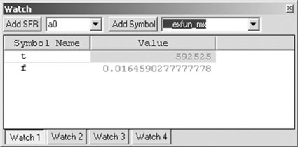
We once more reduced the FFT execution time from 20 ms to 16.4 ms. This is a further 20-percent performance improvement.
Fine-Tuning the PIC32: Final Notes
As anticipated, the complexity of the cache module is considerable, and the number of additional possible “tricks” is practically unlimited if you dare dig deeper. I will mention only one last option related to accessing the RAM memory. As it happens, even regular RAM memory access is by default slowed by the presence of a single wait state. Its presence is already greatly mitigated by the cache, and the impact on the overall processor performance can be further reduced by the efficiency of the compiler and its use of the processor registers. Nonetheless, it is worth trying to disable it using the mBMXDisableDRMWaitState() function.
In my experiments, this produced an almost unnoticeable performance improvement, but the mileage can vary greatly with the nature of the application (see Figure 7.12).
After rebuilding the project with the added last fine-tuning step, we obtained an additional 1-percent performance improvement.
In summary, in only four lines of code we have been able to produce an almost unimaginable performance improvement compared to our initial measurements using the default configuration at start-up. We went from 170.62 ms down to 16.45 ms, equivalent to a 10× speed performance boost to our FFT algorithm!
Fortunately, the PIC32 support team has been preparing a shortcut for us, a single simple library function that, from now on, will allow us to perform all of the above optimizations in a single function call:
![]()
A precious little function that fine-tunes the Flash memory and RAM access while unleashing the power of the cache and pre-fetch module of the PIC32. How about renaming it SportTuning() or RacingMode()?
Debriefing
Step by step, today we learned to tune up the engine of the PIC32, first in coarse steps, then gradually in finer steps, until we have been able to squeeze the most performance out of the machine. Keep in mind that the tuning process is very much dependent on the task at hand. Different applications will respond differently to each turn of the various “control knobs” we have touched today. Also, the result obtained is by no means representative of the fastest FFT implementation possible on a PIC32. In fact, we have deliberately chosen not to modify the original algorithm in any way, to highlight instead the relative performance gains obtained by our use of various hardware features available on the PIC32MX architecture. In the process we have also learned something new about the peripherals set and, in particular, the PIC32 timer modules that allow us to combine them in pairs to produce 32-bit timers.
Notes for the Assembly Experts
Once more we have resisted the temptation to use any hand optimization, avoiding any use of the assembly language. In reality, those of you who want to learn more about the PIC32 assembly will soon discover that there are powerful instructions in the PIC32 instruction set that we could have used to further boost the performance of the microcontroller in many signal processing applications. In particular, I am referring to the multiply and accumulate instructions, or multiply and add (MADD), as they are known in MIPS lingo.
Notes for the PlC® Microcontroller Experts
Thanks to the cache and the pre-fetch mechanism, the PIC32 can execute “almost” one instruction per clock cycle, even when operating at the maximum clock frequency while using a low-power Flash memory. The operative word here is “almost,” since we cannot be sure that this happens all the time. The cache is inevitably going to generate misses here and there; for example, the MCU will have to wait from time to time while a group of words is loaded by the pre-fetch mechanism or a new word of data is loaded into the cache. The more your code revolves around a short loop that fits entirely in the PIC32 cache memory (256 bytes), the smaller the percentage of misses you will experience. By the way, although we don’t have the time and space to cover the subject in the necessary depth in this book, most of the control registers inside the cache module are actually there to allow us some insight into the workings of the cache and to help us “profile” a specific piece of code.
So, can we claim that the PIC32 is a 72 MIPS machine, meaning that is it really executing 72 million instructions per second? I think the wise answer is “mostly” yes, but … it depends on your code and how well you can get the cache to work for you.
Tips & Tricks
One powerful tool, available as part of the MPLAB IDE, is the Data Monitor and Control Interface, or DCMI for friends and fans. You can activate it by selecting Tools | DCMI on the MPLAB IDE main menu. When used in combination with any of the in circuit debuggers and even the MPLAB SIM simulator, it can provide us with a window into the device data space by producing graphics but also letting us “interactively” modify the data with a sort of configurable graphical user interface (GUI). In particular, when playing with the FFT you might be interested in checking the shape of the input signal we synthesized (sinusoid) and in visualizing the output of the FFT routine. Once in the DCMI window, follow the next few steps in exact order:
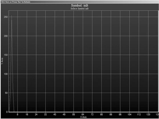
Now set a breakpoint on the line containing the OpenTimer45() call, just following the inB[] buffer initialization, and run the program.
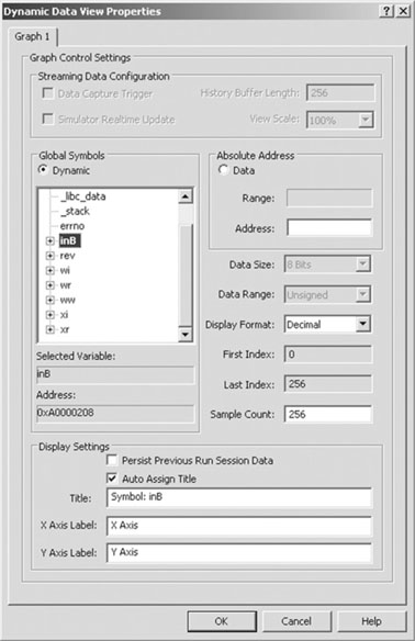
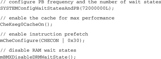
As the program halts you should see the content of the inB[] buffer nicely visualized inside the Dynamic Data View window (see Figure 7.14).
It’s a 2 Hz sinusoid, or I should say a sinusoid whose period is half the input sample count.
Now we can set a second breakpoint on the line where the ReadTimer45() function is called, after the FFT is performed and the scaling is performed to visualize the output. Remember that the output of an FFT contains only half the size of the input number of samples, so you can change the Sample Count field of the visualization to 128 instead of the default value (256) automatically offered by the DCMI. Also maximize the window to obtain a better detail (see Figure 7.15).
As you can see, the one and only peak in the signal power spectrum is easily found on the X-axis (considering the sample count starts from 1) at the position that would correspond to a frequency of 2 Hz (or two periods within the input sample count). Verify that this is exactly what we have designed the input test signal to be!
Exercises
Books
Sweetman, Dominic, See MIPS Run, second edition (2006). This is a must-read if you want to truly understand the most advanced features of the PIC32 MIPS core. The second edition is recommended because it focuses on the more modern implementations of the MIPS cores and adds notes on Linux kernel implementation details. (Don’t try this at home on the PIC32MX … not just yet.)
Links
http://en.wikipedia.org/wiki/FFT. Helpful in learning more about uses of and methods to perform a Fast Fourier Transform.
http://en.wikipedia.org/wiki/Spectral_music. FFt can be fun! Think graphics, but also think music composition.
http://en.wikipedia.org/wiki/Window_function. No, we’re not talking about those windows; these windows can dramatically change your views!
http://wn.wikipedia.org/wiki/CPU_cache. The PIC32MX is the first PIC microcontroller to use a cache mechanism. It is worth looking deeper in the subject to understand which decisions and compromises the designers of the PIC32 had to make to maximize performance while delivering an inexpensive product.