Chapter 13. Interfacing and Data Communications
13.1. Interfacing
The term interfacing is used to describe the connection between a transducer or some other external device and the microcomputer. Interfacing circuits may be required to deal with various levels of incompatibility:
- Incompatible voltage levels
- Changing current levels
- Electrical isolation
- Timing of data transfers
- Digital-to-analog and analog-to-digital conversions
Mechanical or electronic devices requiring connection to the microprocessor unit can be anything from the output screen or monitor, the keyboard, and external instruments. Two main problems are usually encountered when interfacing such devices:
- Most devices do not operate at the same speed as the microprocessor
- There may be more than one device which requires servicing at any one time
A port is a connection from the outside world to the microprocessor (Figure 13.1). The purpose of an input port is to transfer information from the outside world to the microprocessor. An output port provides information to the outside world from the microprocessor. Each port has an address and is thus connected to the address bus and information to or from the port is transmitted over the data bus. From the microprocessor's point of view, a port is very similar to a location in memory.
Figure 13.1. Typical I/O ports on a microcomputer.
Ports may be memory mapped, interfacing direct to the computer's RAM, or be assigned a separate port address. An interface adaptor connects the data bus to the I/O device using compatible signals when the port is accessed by the CPU for read/write operations.
12.2. Input/Output Ports
In an 8086-based microcomputer, I/O ports are identified using a 16-bit port number or port address (Table 13.1). Thus, there are a total of 65,536 possible ports numbered 0 to 65,535 (FFFF). The CPU uses a signal on the control bus to specify that the information on the address bus and data bus refers to a port and not a regular memory location. The port with the specified number then receives or transmits the data from its own internal memory.
Table 13.1. Port addresses
| Port number | I/O device |
|---|---|
| 0000–001F | Direct memory access controller |
| 0020–003F | Programmable interrupt controller |
| 0040–005F | System timer |
| 0060–0060 | Standard 101/102-key keyboard |
| 0061–0061 | System speaker |
| 0062–0063 | System board extension for ACPI BIOS |
| 0064–0064 | Standard 101/102-key keyboard |
| 0065–006F | System board extension for ACPI BIOS |
| 0070–007F | System CMOS/real-time clock |
| 0080–009F | Direct memory access controller |
| 00A0–00BF | Programmable interrupt controller |
| 00C0–00DF | Direct memory access controller |
| 00E0–00EF | System board extension for ACPI BIOS |
| 00F0–00FF | Numeric data processor |
| 0170–0177 | Intel® 82801BA Ultra ATA storage controller—244B |
| 0170–0177 | Secondary IDE controller (dual FIFO) |
| 01F0–01F7 | Intel® 82801 BA Ultra ATA storage controller—244B |
| 01F0–01F7 | Primary IDE controller (dual FIFO) |
| 02F8–02FF | Communications port (COM2) |
| 0376–0376 | Intel® 82801 BA Ultra ATA storage controller—244B |
| 0376–0376 | Secondary IDE controller (dual FIFO) |
| 0378–037F | ECP printer port (LPT1) |
| 03B0–03BB | Intel® 82815 graphics controller |
| 03C0–03DF | Intel® 82815 graphics controller |
| 03F0–03F5 | Standard floppy disk controller |
| 03F6–03F6 | Intel® 82801 BA Ultra ATA storage controller—244B |
| 03F6–03F6 | Primary IDE controller (dual FIFO) |
| 03F7–03F7 | Standard floppy disk controller |
| 03F8–03FF | Communications port (COM1) |
| 04D0– 04D1 | Programmable interrupt controller |
Input ports generally require servicing (i.e., their data to be read) at irregular intervals, and further, their signals may only appear momentarily. Techniques such as polling, interrupts, and direct memory access are used to service ports as required.
13.3. Polling
The easiest method of determining when a device requires servicing is to ask it. This is called polling. In this method, the CPU continually and sequentially interrogates each device (Figure 13.2). If a device requires servicing, then the request (or bus access) is granted. If the device does not require servicing, then CPU interrogates the next device.
Figure 13.2

Polling is very CPU intensive since the processor must spend a large amount of time interrogating devices that do not require servicing. However, the procedure may be easily implemented in software making it flexible and convenient. In some circumstances, polling may be actually faster than more direct methods of interfacing (interrupts and DMA).
Interfacing in a Multitasking Environment
Interfacing in a multitasking operating system like Windows brings with it many issues that may require special attention. The three main methods of obtaining data from an interfaced device (polling, interrupts, and DMA) cannot be guaranteed to occur at a particular time. This causes problems for time-critical applications in which the time at which the data is recorded is important, and also for applications requiring large amounts of data to be rapidly collected.
Steps can be taken to minimize the problems. I/O devices such as general purpose data acquisition cards make use of virtual device drivers employing commands with low-level privileges, hardware buffering, and bus-mastering DMA can be used with some effect but cannot remove the limitations of the overall system placed on it by the multitasking environment.
In some applications, where the cost and effort are appropriate, interfacing can be done at the transducer and the data buffered and transferred to the microcomputer at a time convenient to the microprocessor. In these systems, the transducer contains a microprocessor of its own and is programmed using an erasable programmable read only memory (EPROM). Commands can be sent to the on-board microprocessor to run different internal programs using an ordinary serial communications protocol.
Intelligent transducers contain all the power to obtain the necessary data from the sensor under a variety of conditions, report error conditions, and self-calibrate under the control of a supervisory computer via an Internet, radio, or direct cable connection.
13.4. Interrupts
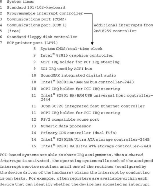
Hardware interrupts are controlled by the 8259 programmable interrupt controller (Figure 13.3). I/O devices managed by hardware interrupts are printers, keyboard, and disk drives. The IRQ allocation is a hardware device interrupt number simply used to conveniently label the devices making use of the 8259 controller. The lower the IRQ, the higher the priority (see Figure 13.4).
Figure 13.3

Figure 13.4. Typical IRQ allocations.
For interfacing applications, the time taken to register and process an interrupt (interrupt latency) can lead to the need for the I/O device to be heavily buffered. In addition, time-critical interfacing applications may not work as desired.
13.5. Direct Memory Access (DMA)
In normal data transfer, data is transferred from one memory location to another through registers in the CPU. The CPU has to hold the data temporarily while it switches the control bus signal from a read to a write since the data bus cannot be in a read state and a write state at the same time. This temporary storage of data and resulting transfers into and out of the CPU is time consuming and wasteful for interfacing applications that require rapid accumulation of data and precise timing.
In direct memory access, or DMA, data can be transferred directly between memory and the I/O port (Figure 13.5) since I/O memory locations are independent of RAM memory. DMA requires full control of the address, data, and control buses. When a DMA transfer is to occur, a DMA controller 8237 IC requests control of the bus from the CPU. The CPU promptly grants control and suspends any bus-related activity of its own. The DMA controller then transfers data from port to memory or memory to port directly, without any stack or register overhead operations that would normally be required by the CPU to accomplish the same task. The DMA acts as a third party to the data transfer. The latency time associated with DMA transfer is only a few CPU cycles.
Figure 13.5
The 8237 DMA controller has a number of independent channels, each of which is assigned to a particular device. Channel 2 is usually assigned to the floppy disk controller. DMA can take place as a single byte or word, a block of bytes, or on demand up to a set number of bytes. DMA transfers can be initiated by a hardware request (via DREQ input on the 8237) or a software request using a request register.
With a PCI bus, DMA management can be performed not only with the DMA controller but also by the device requiring DMA access. In such systems, the device that gains control of the bus is called the bus master. For interfacing applications, the combination of bus-mastering DMA and a high-speed PCI bus ensures that data transfer occurs as fast as possible from the I/O device to memory. Further, bus-mastering DMA does not require the allocation and usage of DMA channels since the DMA controller is not involved. Bus-mastering DMA is referred to as first-party DMA since the I/O device itself is handling all the data transfer.
13.6. Serial Port
Most microcomputers are fitted with one and often two serial ports. These serial ports are labeled COM1 and COM2. The numbers 1 and 2 are for our “external” convenience only. The actual “internal” port numbers or addresses are 3F8 for COM1 and 2F8 for COM2.
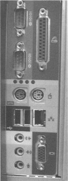
The COM ports can usually be found on the back panel of a microcomputer and may take the form of either 25- or 9-pin connectors (Figure 13.6). (The 9-pin connector was introduced to save space when the parallel and serial ports were placed on a single interface card.) These pins are connected to buffers which convert the pin voltages used for data transmission over external cables (usually using the RS232 standard) to TTL levels used for data transfer within the computer. The internal signals are generated by a special communications IC called a UART.
Figure 13.6. Serial port pin connections for RS232 communications.

The serial port is most often used for data communications. Hence, one of the signal lines carries data either being transmitted from, or received by, the computer. The other signals are used to control the flow of data and to establish a communications link between the two serial ports on two different computers. Often, the serial ports are connected by a modem which converts digital data into analog signals for transmission over a telephone line.
The handling and control of transmission is done by setting and reading the binary data that appears in the internal registers of the UART. Each of these registers has an address (i.e., the port address) in the port address space of the computer.
13.7. Serial Port Addresses
The port addresses for IBM compatible microcomputers have been standardized for many years (Table 13.2). Here, 3F8 and 2F8 are the base address of each port. It is customary to refer to the first address as the base address.
Table 13.2.
| Purpose | COM1 | COM2 |
|---|---|---|
| Tx, Rx data | 3F8 | 2F8 |
| Interrupt enable | 3F9 | 2F9 |
| Interrupt ident | 3FA | 2FA |
| Line control | 3FB | 2FB |
| Modem control | 3FC | 2FC |
| Line status | 3FD | 2FD |
| Modem status | 3FE | 2FE |
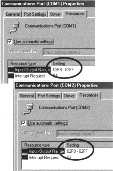
In Windows, it is easy to obtain the base address for the COM ports (see Figure 13.7). In Control Panel, select System, and then Device Manager. Select COM ports and then properties.
Figure 13.7
Each port address is a register that allows the serial port to be initialized and operated on by software commands. That is, the serial port controller ship, the 8250 UART, is programmable in the sense that its operation can be controlled by software rather than hard-wired circuitry.
When a serial port interface card is added to a computer, the base address must be set, either by a jumper on the card, or by software. This allows the card to be configured as COM1 or COM2 (or even COM3 or COM4) as desired.
13.8. Serial Port Registers
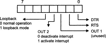
The LCR (line control register) is shown in Figure 13.8. The LSR (line status register) is shown in Figure 13.9. The MSR (modem status register) is shown in Figure 13.10. The d flags are set if the state of the control lines has changed since they were last read. The MCR (modem control register) is shown in Figure 13.11. The MCR is not set by the 8250 UART itself. We must set bits in it to control the UART operation and/or the modem control lines.
Figure 13.8. Line control register.
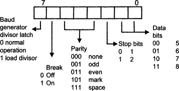
Figure 13.9. Line status register.
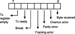
Figure 13.10. Modem status register.
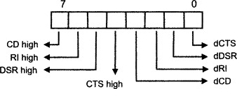
Figure 13.11. Modem control register.
13.9. Serial Port Registers and Interrupts
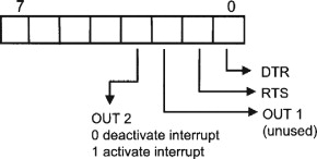
It is most common to operate the serial port (i.e., such as the 8250 UART) through the use of interrupts. However, this need not always be the case. The 8250 has four internal interrupt signals that can be connected through to the CPU's IRQ interrupt line via an INTR pin on the UART. The OUT2 bit in the modem control register specifies whether or not to connect the UART INTR output to the CPU's IRQ line. In this way, the internal interrupts generated by the UART can be optionally used by the CPU. Note: COM1 usually uses IRQ4 and COM2 IRQ3 on the CPU.
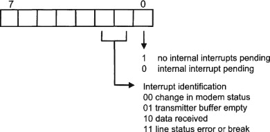
Figure 13.12 shows an IER (interrupt enable register). A one in the corresponding bit position enables the internal interrupt. This will not be registered at the CPU IRQ line unless OUT2 in the MCR is also set to one. Figure 13.13 shows an IIR (interrupt identification register).
Figure 13.12. Interrupt enable register.
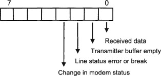
Figure 13.13. Interrupt identification register.
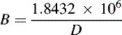
13.10. Serial Port Baud Rate
The baud rate is a measure of the number of bits per second that can be transmitted or received by the UART. This rate is regulated by a clock circuit which, for most UARTS, is on the chip itself and can be programmed.
![]()
where D is called the baud rate divisor and must be loaded into the UART.
For example, a baud rate of 9600 is required. What is the divisor D?

- Bit 7 of the LCR must be set to 1
- The LSB of D is written to the port base address (e.g., 3F8 for COM1)
- The MSB of D is written to the port base address + 1 (e.g., 3F9)
- Bit 7 of LCR is cleared (and perhaps also set for other parameters such as baud rate, stop bits, etc.)
- Check port base address + 1 for the desired interrupt settings
The UART clock must operate at 16 times the desired baud rate. The clock is based around the operation of a crystal oscillator which, in the case of a 8250 UART, is set to a constant 1.8432 MHz. This clock signal is stepped down through a series of counters to obtain the desired clock rate for the chip to give the desired baud rate.
13.11. Serial Port Operation
Although it is possible to write and read from the serial port registers directly, it is more convenient to use either application's program languages or BIOS service routines. Most applications' languages have statements or functions available that facilitate the programming of the serial port. For example, the
- OPEN "COM1:9600,N,8,1" AS #1
statement in BASIC allows the serial port to be configured without a detailed knowledge of the actual port addresses. However, for interfacing applications, direct manipulation of the registers is required. For example, the BIOS service routines on an IBM compatible PC do not provide a way to set RTS for hardware handshaking.
In Visual Basic, it is necessary to make use of the serial port object. MSComml has properties that can be set in code that allow the serial port to which it is assigned to be configured.
- ·MSComml . Settings = "9600,E,7,1"
- ·MSComml . InputLen = 0
- ·MSComml . RTSEnable = True
- ·MSComml . DTREnable = False
- ·MSComml . PortOpen = True
These high-level instructions ultimately result in a series of assembly language instructions that call BIOS service routines through the interrupt system.
The serial port initialization parameters are baud rate, parity, stop bits, data bits. They are combined into an 8-bit number which is loaded into AL prior to calling the interrupt.
The service to be called (0 for initialize serial port) is placed into AH. Parameters for the service are placed in AL. The interrupt is called, and the results placed in AL (or AX for service 3), for example,
- mov AH, 0
- int 14H
13.12. Parallel Printer Port
The parallel port normally found on microcomputers is generally used for printer output, although there are some input lines that are used to report printer status (such as paper out etc.). The Centronics printer interface consists of eight data lines, a data strobe, acknowledge, three control, and four status lines (Figure 13.14).
Figure 13.14
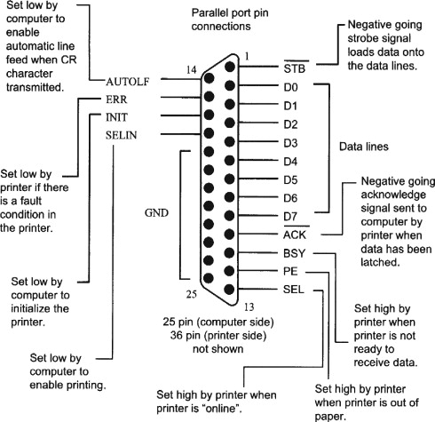
The printer port is driven by the parallel port adaptor. In the adaptor, there are three registers that are assigned I/O port addresses. The byte to be printed is held in the data register that is at the port base address. The printer status register contains the information sent to the computer by the printer and has an address of base + 1. The printer control register has address base + 2 and contains the bit settings for computer control of printer functions.
13.13. Parallel Port Registers
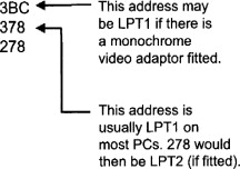
Printer port data register (base) 378 is shown in Figure 13.15. Printer port status register (base + 1) 379 is shown in Figure 13.16. Printer port control register (base + 2) 37A is shown in Figure 13.17. The base address for the parallel printer port can be either of those in Figure 13.18.
Figure 13.15. Printer port data register (base) 378.
![]()
Figure 13.16. Printer port status register (base + 1) 379.
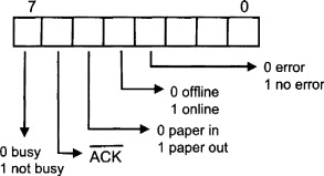
Figure 13.17. Printer port control register (base + 2) 37A.

Figure 13.18. Base address for the parallel printer port.
In Windows, the base address of the parallel port is obtained through the Device Manager in the Control Panel (Figure 13.19). Select LPT1 and then Properties.
Figure 13.19

13.14. Parallel Printer Port Operation
Although it is possible to write directly to the parallel printer port registers, it is customary to use the BIOS service routines available through the computer's operating system. Mostly this is done indirectly through high-level program statements like PRINT. However, it is possible (and sometimes desirable) to call the BIOS routines directly from an assembly language program.
BIOS routines are called through interrupt 17H. Three services are available and are selected by the value placed in AH. For writing a byte to the printer, the data to be printed is put into AL. The DX register is set to indicate the LPT port to use (0 for LPT1):
- AH—BIOS service
- 00—Write byte
- 01—Initialize printer
- 10—Report printer status
After the service has been executed, the contents of the printer status register are reported in AL.
When the printer port is being used through the BIOS service routines or being accessed directly, the following sequence is required to write the data:
- The data to be written is placed in the printer port data register. That is, the byte is written to the printer port base address.
- The readiness of the printer to accept data is confirmed by testing the bits in the printer port status register.
- The STB line is then pulsed low by writing a one to bit 0 of the printer port control register. This transfers the data from
the printer port data register to the data lines on the port connector (Figure 13.20).
Figure 13.20. Centronics-type parallel connector.

Note: Although the parallel printer port is usually used for printing (i.e., output), there is no rule against using the port for input and output for other peripherals. The IEEE 1284 (introduced in 1994) standard defines five modes of data transfer: compatibility mode (standard mode); nibble mode (4 bits in parallel using status lines for data); byte mode (8 bits in parallel using data lines); EPP (enhanced parallel port—used primarily for CD-ROM, tape, hard drive, network adapters, etc.), and ECP (extended capability port—used primarily by new generations of printers and scanners).
13.15. Communications
Once an analog signal has been digitized by the ADC, the digital information must then be passed to a port of a microcomputer for subsequent placement on the data bus. An inexpensive, readily available method is by serial communications using the serial port. Other common methods are to use an ADC interface card that interfaces directly to the computer bus system, and the GPIB parallel data bus.
Steps in serial transmission of a byte of digital data (Figure 13.21) are
- Byte is converted into sequential series of bits
- Bit transmitted over signal wire
- Bits reassembled into bytes
Figure 13.21

The digital information coming from the ADC is a series of bytes, generated one after the other, as the input signal is repeatedly sampled. In the serial method of transmission, the bits that comprise each byte are sent one at a time, in sequence, along a single wire and then reassembled into a byte after transmission.
13.16. Byte-to-Serial Conversion
At the transmission end of the process (Figure 13.22), the byte of data is sent bitwise over a signal wire. This is done using a shift register in a special integrated circuit called a UART (universal asynchronous receiver/transmitter).
Figure 13.22
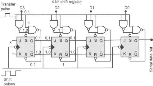
A shift register can be made using cascaded JK flip-flops. A positive transfer pulse loads the asynchronous inputs R and S with the data to be shifted. For example, if D = 0, then on the transfer pulse, S = l, R = 0, and Q = 0. If D = l, then S = 0, R = 1, and Q = 1. Thus, after the transfer pulse, the parallel data is transferred to the J input of each flip-flop. When the transfer pulse goes low, R and S are both at 1 which is the no change state, and on the clock or shift pulse, data is transferred along the chain from Q to J, the serial output bit stream appearing as the last output Q. At the receiving end, the serial bit stream is converted to parallel 8- bit data by a reverse of the preceding. Data is clocked in, and then a transfer pulse transfers the data to the parallel outputs.
Now, for long distances, the bit stream is not usually transmitted directly over wires since the binary signals are easily distorted with distance. This, together with the requirement that the transmitter and receiver need to be synchronized, means that alternative arrangements are required to actually transmit the data over distances of more than about 15 m.
13.17. RS232 Interface
The RS232 interface standard defines the necessary control signals and data lines to enable information to be transmitted between computer equipment (or data terminal equipment, DTE) and the modem (or data communication equipment, DCE). The modulated carrier signal is transmitted over a two-wire telephone network by the connecting modems (Figure 13.23).
- RTS is raised high by the sending computer indicating that data is ready to be sent.
- The transmitting modem sends a carrier signal to the receiving modem which raises DCD on its connection to the receiving computer which is thus notified of the existence of a carrier signal.
- The transmitting modem waits for a preset period for the receiving computer to get ready to receive data.
- The transmitting modem raises CTS signaling to the sending computer that it may now begin to send data.
- The transmitting modem receives digital data from the sending computer on the TD line and modulates the carrier wave accordingly. The receiving modem demodulates the carrier and puts digital data on the RD line connection to the receiving computer.
- When the sending computer has finished sending the data, it clears the RTS signal to the transmitting modem which then drops the carrier and clears its CTS signal. The receiving modem detects loss of carrier signal and it drops its DCD line to the receiving computer.
Figure 13.23
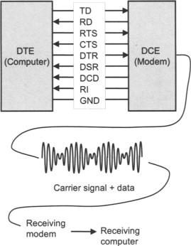
A modem converts or “modulates” digital information into a form suitable for transmission over the telephone network. The receiving modem demodulates the signal back into digital data for use by the receiving computer. Modems transmit information using a sine wave carrier that is modulated (either through amplitude, frequency, or phase) to carry binary information.
13.18. Synchronization
Start and stop bits frame the data bits (Figure 13.24). When the signal line is not sending data, it is idle and held at mark or logic high. The start bit is low or space and thus, when the receiver sees a transition from mark to space, it knows that the next bit to be received is the LSB of the data being transmitted. After all the data bits have been received, the receiver interprets the next bit to be a stop bit which is mark. If the bit actually received is not mark, then the receiver knows that an error has occurred.
Figure 13.24

The receiver clock is usually made 16 times the bit rate. When a mark to space transition is detected, the receiver counts eight clocks. If the signal is still at space, then it is assumed that the signal is a valid start bit. The receiver counts off another 16 clocks and then samples the data until all the data bits and stop bit(s) have been received. The bit sampling thus takes place in the center of the signal levels.
After the data bit and before the stop bit, there may be a parity bit which is used as a check for data validity. In even parity, the total number of ones (including the parity bit) is made to be an even number (and vice versa). The receiver computes its own parity bit when a byte is received and compares it with that appended by the sender. A mismatch indicates a parity error.
The rate of transmission is the data bit rate which is called the baud rate. Generally, the baud rate is the same as the bit rate; however, some transmission systems are capable of sending more than one data bit (e.g., amplitude and phase modulation) into a transmission bit and the bit rate is thus higher than the baud rate.
13.19. UART (6402)
The 6402 UART takes in parallel byte data into the transmitter buffer register at the inputs TBR1-8 (Figure 13.25). This data is transferred into the transmitter register for shifting. The output bit stream appears at transmitter register output (TRO). Similarly, serial data is read in at receive register Input, converted to a character in the receive register, and appears at receive buffer register outputs RBR1-8. The transmitter part of the circuit automatically adds start, stop, and parity bits according to logic levels applied at control inputs. The receiver checks for parity and stop bit errors and issues logic levels at various indicator outputs.
Figure 13.25
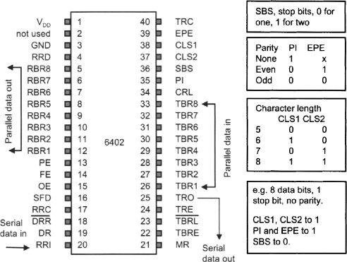
When TBRL goes low, data is read from the input pins TBR1-8 and transferred to the transmitter buffer register. When TBRL goes from low to high, data is transferred from the transmitter buffer register to the transmitter register whereupon data is shifted and transmitted out on TRO.
If RRD is held low, then the data on RBR1–8 is that last read from the input stream at RRI. A high level on DR indicates that the data read is available at RBR1–8. Once read, DR needs to be reset by a negative pulse to DRR.
A description of the pin functions on the 6402 UART follows:
- RRD, receiver register disable—A high level forces RBR1 to RBR8 to a high impedance state.
- RBR8–RBR1, receiver buffer register outputs—Parallel byte data is output here.
- PE, parity error—High level indicates that the received parity does not match the parity set by the control bits. When the parity is inhibited (PI) this pin is held low.
- FE, framing error—High level indicates that the first stop bit is invalid.
- OE, overrun error—High level indicates data received flag was not cleared before the last character was transferred to the receiver buffer register.
- SFD, status flag disable—High level input forces the outputs PE, FE, OE, DR, TBRE to high impedance.
- RRC, receiver register clock—Set to 16 times the baud rate.
- DRR, data received reset—A low level clears the output DR to low.
- DR, data received—A high level indicates character has been received and transferred to the receiver buffer registers.
- RRI, receiver register input—Serial data is clocked into the receiver buffer registers from here.
- MR, master reset—High level clears PE, FE, OE, and DR and sets TRE, TBRE, and TRO to high. MR should be pulsed high after power-up to reset the UART.
- TBRE, transmitter buffer register empty—Indicates that the transmitter buffer register has transferred its data to the transmitter register and is ready to accept new data.
- TBRL, transmitter buffer register load—A low level transfers data from the inputs TBR1–8 to the transmitter buffer register.
- TRE, transmitter register empty—A high level indicates that transmission of a character, including stop bits, has been completed and that the transmitter register is now empty.
- TRO, transmitter register output—Serial data output line.
- TBR1–8, transmitter buffer register inputs—Parallel data is loaded into the transmitter buffer registers at these inputs.
- CRL, control register load—High level loads the control register with parity, character length, and other settings.
- TRC, transmitter register clock—Set to 16 times the baud rate.
The more versatile 8250 (16450) UART extends the functionality of the basic 6402 by having programmable registers that set the baud rate, parity, and stop bits and an interrupt controller. High-level commands in an application program set the appropriate bits in the internal registers (see Section 13.5). Later 16550 UARTS feature first-in, first-out (FIFO) buffers which allow data transfer to happen at maximum speed while the processor is momentarily occupied by other tasks.
13.20. Line Drivers
RRI and TRO on the 6402 UART are the serial input and output lines. The polarity of the signals is +5V for mark, or high, and 0V for space, or low. However, the transmission of serial data along the wire in an RS232 transmission interface requires −15 to −12V for mark and +12 to +15V for space. Line drivers are used to convert the logic levels required by the UART to those required at the RS232 interface pins TD and RD.
A very useful IC is the 232CPE dual RS232 transmitter/receiver (Figure 13.26). This IC requires a single +5-V supply and generates +10V and −10V necessary to drive the RS232 signal lines. (Note: Handshaking signals CTS, RTS, DSR, etc. are also at +10V, −10V.)
Figure 13.26. Transmitting: T TL input, RS232 output. Receiving: RS232 input, TTL output. The external capacitors are used by the internal voltage doublers to obtain ±10-V RS232 signals.
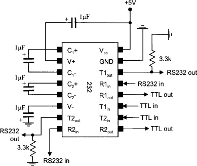
The 232 takes either TTL or CMOS logic levels as inputs and provides ±10V at the RS232 outputs. It also receives RS232 inputs and provides equivalent TTL or CMOS levels as an output. There are two separate channels available for both receiving and transmitting.
13.21. UART Clock
The 6402 has two separate clock inputs but, normally, these are driven by the same clock so that the transmit and receive baud rates are the same. The clock frequency is to be 16 times the baud rate. The 6402 chip does not have a programmable baud rate divider (as in the 8520) so the desired clock frequency must be supplied externally using a binary counter.
A crystal oscillator can be used in conjunction with a high-speed inverter to produce a square wave output which can be stepped down to the desired frequency with a binary counter (Figure 13.27).
Figure 13.27.

The crystal's (Figure 13.28) piezoelectric properties are electrically equivalent to an inductance in series with a capacitance at its resonant frequency. The circuit shown is a CMOS inverter implementation of a Colpitts oscillator. The input/output states of the inverter oscillate at the resonant frequency of the crystal.
Figure 13.28

13.22. UART Master Reset
MR in Figure 13.29 is the master reset. High level clears PE, FE, OE, and DR and sets TRE, TBRE, and TRO to high. MR should be pulsed high after power-up to reset the UART. A simple delay circuit using a capacitor and a NAND gate can be used to send a short positive pulse to MR on power-up. The time constant is simply the product RC, and values of R1 = 100 kΩ and C = 4.7 μF give a time constant of about 0.5s.
Figure 13.29
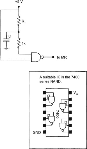
Initially, NAND output is at 0V. When Vcc is applied, the NAND output goes to 1 since one input is at +5V and the other at 0V. As the capacitor charges up through R1, voltage at upper input to the NAND rises, and after a time characterized by R1C, the NAND gate flips from 1V to 0V. The 1-kΩ resistor limits the current into the NAND for protection.
13.23. Null Modem
The RS232 serial protocol was designed to transmit data over a considerable distance using the telephone network but may also be used for local communication to and from a device attached to the serial port of a computer. The exact same control lines may be used to regulate the flow of data between the connected equipment without the use of a modem; however, there is a problem: If both devices are connected pin to pin and attempt to send data over the transmit line, then no signals will appear on the receive lines. Thus, the transmit and receive lines must be crossed over. This type of connection is called a null modem (Figure 13.30).
Figure 13.30
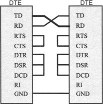
Tying DTR, DSR, and DCD together in effect tells the computer that the modem is connected to a telephone line upon which there is a valid carrier signal and data can be either sent or received. Of course, there is no modem present at all, hence the term null modem. TD, RD, and signal ground are the minimum requirements for a serial connection between two computers, the other connections may be required if the communications software on the computers tests the modem status before sending or transmitting data. In the preceding example, the connections between RTS and CTS, and DTR, DSR, and DCD, cause the computer to regard the connection as occurring between modems even if no modem is used at all. For instance, the computer that is sending data first raises its RTS line, which is now directly connected to CTS. The sending computer thus immediately receives a CTS signal from its own RTS and begins to transmit data on TD. The receiving computer receives this data on its RD line.
13.24. Serial Port BIOS Services
BIOS services may be used to initialize and use the serial port. These services are available through interrupt 20 (14H). Parameters for the interrupt are specified in the AL register. The serial port is specified in DX. The four services available are shown in Table 13.3. The initialization parameters are shown in Table 13.4.
Table 13.3. BIOS services
| 0 | Initialize serial port. | The serial port initialization parameters are baud rate, parity, stop bits, data bits. They are combined into an 8-bit number that is loaded into AL. |
| 1 | Send one character. | The 8-bit data to be transmitted is placed in AL. After transmission, a status code is placed in AH. |
| 2 | Receive one character. | The received character is placed in AL. A code is placed in AH to report status. |
| 3 | Read serial port status. | The status returned by services 0–2 and that reported by service 3 are in the form of a bit pattern in the AH and AX registers respectively. A one in any bit position indicates the condition or error returned. |
Table 13.4.
| Bits 7 6 5 | Baud rate | Bits 4 3 | Parity | Bit 2 | Bit 1 0 | No. stop bits | Data bits |
|---|---|---|---|---|---|---|---|
| 0 0 0 | 110 | 0 0 | None | 0 | 0 0 | One | Unused |
| 0 0 1 | 150 | 0 1 | Odd | 1 | 0 1 | Two | Unused |
| 0 1 0 | 300 | 1 0 | None | 1 0 | 7 | ||
| 0 1 1 | 600 | 1 1 | Odd | 1 1 | 8 | ||
| 1 0 0 | 1200 | ||||||
| 1 0 1 | 2400 | ||||||
| 1 1 0 | 4800 | ||||||
| 1 1 1 | 9600 |
The service to be called is placed into AH (Table 13.5). Parameters for the service are placed in AL. The interrupt is called, and the results placed in AL (or AX for service 3).
- mov AH, 0
- int 14H
Table 13.5.
| AH | AL | ||
|---|---|---|---|
| 7 | Time out | 7 | Receive signal detect |
| 6 | Transfer shift register empty | 6 | Ring indicator |
| 5 | Transfer holding register empty | 5 | Data set ready |
| 4 | Break-detect error | 4 | Clear to send |
| 3 | Framing error | 3 | Delta receive signal detect |
| 2 | Parity error | 2 | Trailing edge ring detector |
| 1 | Overrun error | 1 | Delta data set ready |
| 0 | Data ready | 0 | Delta clear to send |
Note: "Delta" bits indicate a change in the indicated flags since the last read.
13.25. Serial Port Operation in BASIC
Serial communications can be easily implemented in BASIC. This language provides statements that allow programming of the UART without reference to the actual I/O port memory addresses. The serial port initialization parameters are set using the OPEN statement:
- OPEN "COM1:9600,N,8,1" AS #1
which initializes COM1 at 9600 baud, no parity, 8 data bits, 1 stop bit. Data is written to or read from a "file" numbered "1."
To read 1 byte from COM1, we write: A$=INPUT$ (1, #1)
The byte is read from the receive buffer in the UART and converted to an ASCII character and then assigned to a string variable A$. To display the decimal number actually read, we can use the ASC function:
- PRINT ASC(A$)
The INPUT$ function is the preferred method of reading data from the serial port. Other statements such as INPUT and LINE INPUT may work but may give unpredictable results if the data in the input stream contains ASCII control characters such as LF and CR. If we were to use INPUT, then the input would stop when the incoming data contained a comma or a CR character. This is OK for reading in data from the keyboard but not from a file where we may wish to capture all the data.
In Visual Basic (VB), the procedure is very similar. The COMM port object is placed on a form, in the example that follows, the form is called frmMainMenu and the COMM port object is called MSComml.
MSComml has properties that can be set in code that allow the serial port to which it is assigned to be configured.
- frm_MainMenu . MSComml . Settings = "9600,E,7,1"
- frm_MainMenu . MSComml . InputLen = 0
- frm_MainMenu . MSComml . RTSEnable = True
- frm_MainMenu . MSComml . DTREnable = False
- frm_MainMenu . MSComml . PortOpen = True
Methods available to the serial port object allow characters to be read and assigned to a variable, or the value of a variable to be written and transmitted from the computer:
- ReadChar = frm_MainMenu . MSComml . Input
- frm_MainMenu . MSComml . Output = WriteString + vbCr
13.26. Hardware Handshaking
Although at first sight reading the serial port using BASIC appears fairly straightforward, difficulties arise when the data cannot be read fast enough and the input buffer overflows. The buffer holds 255 characters (i.e., 1 character = 1 byte). Handshaking (either software codes or hardware signals) is used to halt transmission of data from the sending computer until the receiving computer has emptied the buffer. Various functions are available in BASIC to allow either software or hardware handshaking.
- LOC(x) returns the number of characters in the input buffer for file number “x”
- LOF(x) returns the number of character spaces available in the input buffer
- EOF(x) returns (–1) if the buffer is empty or 0 if it is full
Figure 13.31 shows an MCR (modem control register). For COM2, the MCR port address is 2FC.
Figure 13.31
For the serial data acquisition circuit, hardware handshaking must be used, since there is no method of interpreting software codes such as XON and XOFF. The RTS line offers the most convenient form of hardware handshaking. RTS is arranged to go logic high (–10V on RS232 signal lines) when the buffer is full and then low when the buffer is empty. Now, the RTS signal line is available via the second bit in the modem control register. Setting this bit to zero will actually set RTS to logic high. The BASIC OUT statement can be used to send a byte to an I/O port address. Thus,
- OUT &H2FC, &H8—Set RTS logic high
- OUT &H2FC, &HA—Set RTS logic low
These statements, in combination with the LOC, LOF, and EOF functions, can be used to control RTS. The RTS signal in turn can be wired to halt and resume transmission of data as required.
Note: The BASIC INPUT$ statement makes use of interrupts to read the data from the serial port. Make sure that OUT2 remains set at one when writing data to the MCR.
13.27. RS485
The maximum distance allowed by RS232 is about 15 m which in an industrial environment can be a severe limitation, especially when the computer is located say in a control room some distance away from the transducer. Further, the maximum data transfer rate can be a limitation for fast data acquisition. Standards such as RS422 and RS485 were developed to overcome these limitations and permit greater flexibility and performance for instrumentation applications.
An increase in transmission speed and maximum cable length is done by using voltage differentials on signal lines A and B. For a space, or logic 0, the voltage level on line A is greater than that on line B by 5V. For a mark, or logic 1, the voltage level on line B is greater than that on line A. The receiver inputs on the line driver chip determine whether or not the signal is mark or space by examining the voltage difference between lines A and B. Two signal wires are thus required for data transmission.
Unlike RS232, in which there is usually a connection between two pieces of equipment, the RS485 standard allows for up to 32 line drivers and 32 receivers on the one set of signal lines (Figure 13.32). This is achieved by tri-state logic on the line driver pins.
Figure 13.32
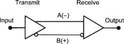
In tri-state logic, pins can be at logic 0, logic 1, or high impedance. The last state effectively disconnects the driver from the line. The high impedance state is set by an “enable” signal on the driver chip.
- Maximum distance 1200 m
- Data rate up to 10 Mbps
- 32 line drivers and receivers on the same line
- TTL voltage levels
Figure 13.33 shows a common RS485 9-pin connector.
Figure 13.33. Common RS485 9-pin connector.

13.28. GPIB
The general purpose interface bus (GPIB) or IEEE 488 interface (Figure 13.34) was developed in 1965 by Hewlett Packard for connecting multiple scientific measuring instruments together. Up to 15 devices may be attached to the interface lines (or bus). One of the devices can be activated as the “controller.” Control can be passed to another device if required.
Figure 13.34
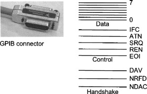
- Eight data lines
- Three data control lines
- Five management lines
- Eight ground lines
The 8-bit data can be transmitted in parallel, each bidirectional line carrying 1 Mbit/s. A maximum total cable length of 20 m with a maximum separation of 4 m between devices is recommended. Bus extenders and expanders can also be used.
Devices may be configured as listeners, talkers, and controllers.
- Listener A device set to be a listener can accept data over the bus from another device. More than one listener at any one time is permitted. A listener receives data when the controller signals it to read the bus.
- Talker A device set to be a talker can send data to another device on the bus. Only one talker can be specified at any one time. The talker waits for a signal from the controller and then places its data on the bus.
- Controller A controller can set other devices as listeners or talkers or to take control. The presence of a controller is optional. For example, if there is only one talker and all other connected instruments are listeners, then no controller is required.
Data is put onto the data bus by a talker when no device has pulled NRFD (not ready for data) low (negative logic). DAV (data valid) indicates that data is ready, and all devices then pull NDAC (no data accepted) low until the data is read. The parallel connection of devices ensures that NDAC goes high again when all listeners have accepted the data.
Each device responds to commands sent over the data bus. Each device can recognize its address when it appears on the data bus. The device address is usually set by dip switches or from software. The management of the bus is done by the controller which typically contains a special purpose IC on a GPIB interface card.
13.29. USB
The range of peripheral devices now connected to personal computers are attached by serial, parallel, and PS/2 ports, and the requirement for ease of use has resulted in the development of the universal serial bus (USB; Figure 13.35).
Figure 13.35
![]()
USB is designed to be a low-cost, expandable, high-speed, serial interface that offers “plug and play” functionality primarily for business and consumer peripherals.
Data transfer rates for the first implementation of USB were up to 12 Mbps. USB 2.0 allows up to 480 Mbps making it suitable for real-time video and audio, high-resolution digital cameras, and data storage devices.
- USB interconnect The connection between USB devices and the host, the data flow protocols, and the manner in which devices are addressed.
- USB devices USB devices are either hubs, which provide attachments to other hubs or actual devices. The host controller queries the hubs to detect the attachment or removal of devices. A unique bus address is assigned by the host when a device is connected.
- USB host controller There is only one host in any USB system. The host controller sends a token packet that describes the type and direction of the data, the device address, and the end-point number. The device that is addressed then receives a data packet and responds with a handshake packet.
The USB transfers signal and power over a four-wire cable. Differential signaling occurs over two of the wires. There are three data rates:
- High speed at 480 Mbps
- Full speed at 12 Mbps
- Low speed at 1.5 Mbps
A maximum of seven tiers is allowed (Figure 13.36). Tier 1 is the root hub and Tier 7 can only contain devices.
Figure 13.36

In the USB system, one device must be the host and this places some restrictions on its use in an industrial setting. A simple modem, for example, can be wired using a null modem connection and be used with a PLC or other RS232-supported transducer. With a USB system, a computer must generally act as a host, even if communication is wanted only from one device to another.
The “on the go”(OTG) supplement to the USB 2.0 standard allows some degree of peer-to-peer communication without the need for a fully featured host.
In RS232 communications, the format of the data is not defined—it is usually ASCII text but need not be so. The USB uses layers of transmission protocols to transmit and receive data in a series of packets.
Each USB transmission consists of
- Token packet
- Optional data packet
- Status packet
The USB host initiates all transactions. The token packet describes the type of communication (read or write and the destination address). The data packet contains the data to be communicated. The handshaking packet reports if the data was received or transmitted successfully.
Table 13.6 shows the USB connections. Running at 5V allows “bus-powered” devices to be connected (no battery or mains power needed).
Table 13.6. USB cable connections
| 1 | Red | 5V |
| 2 | White | D– |
| 3 | Green | D+ |
| 4 | Black | Ground |
USB is designed to be “plug and play.” When a device is plugged into the bus, the host detects its presence by signal levels on the data lines. It then interrogates the new device for its device descriptor, assigns a bus address to the device, and then automatically loads the required device driver. When the device is unplugged, the host detects this and unloads the driver. This process is called enumeration.
Firewire (IEEE 1394) is a serial interface standard originally developed by Apple Computer (ISB was originally developed by Intel). Firewire allows up to 400 Mbps and is a competitor to ISB (when first introduced, Firewire was several times faster than the then USB standard). Like USB 2.0, the main consumer benefit is high speed for video capture from digital cameras and camcorders without the need for dedicated video capture interface cards.
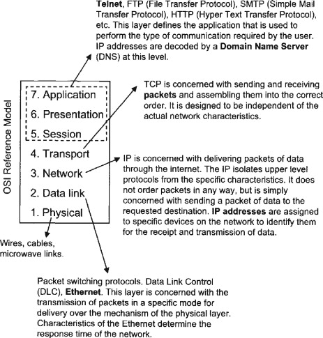
13.30. TCP/IP
TCP stands for transmission control protocol, and IP stands for internet protocol. TCP/IP is a set of protocols that allows computers to communicate over a wide range of different physical network connections (Figure 13.37). TCP/IP provides protocols at two different layers of the OSI reference model. In everyday terms, the World Wide Web (www) and email (SMTP) make use of TCP/IP to communicate over the Internet which in turn runs on a variety of packet switching network systems, the most popular of which is the Ethernet. The actual connections between host computers is done by satellite, coaxial cable, phone lines, etc. For interfacing applications, the Internet is useful for communicating commands and results from a remote sensor but would be unsuitable for a direct interface to the transducer due to the response time of the process.
Figure 13.37