
Chapter 18. Testing Methods
This chapter describes various test techniques, examining their capabilities, advantages, and disadvantages.
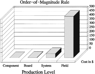
18.1. The Order-of-Magnitude Rule
An accepted test-industry aphorism states that finding a fault at any stage in the manufacturing process costs 10 times what it costs to find that same fault at the preceding stage, as Figure 18.1 illustrates. Although some may dispute the factor of 10 (a recent study by Agilent Technologies puts the multiplier closer to 6) and the economics of testing at the component level, few would debate the principle involved. In fact, for errors that survive to the field, 10 times the cost may be optimistic. Field failures of large systems, for example, require the attention of field engineers, incurring time and travel expenses, and may compromise customer goodwill.
Figure 18.1. The order-of-magnitude rule states that finding a fault at any stage in the manufacturing process costs 10 times what it costs to find that same fault at the preceding stage.
The single biggest cost contributor at every test level is troubleshooting time. Uncovering design problems and untestable circuit areas before production begins can prevent many errors altogether. Similarly, analyzing failures that do occur and feeding the resulting information back into the process can minimize or eliminate future occurrence of those failures.
A prescreen-type tester such as a manufacturing-defects analyzer (MDA) can find shorts or other simple faults much more easily than a functional tester can. In addition, because the functional level generally requires the most expensive and time-consuming test-program development, eliminating a fault class at the earlier stage may obviate the need to create that portion of the functional test program altogether. Equipment and overhead for people and facilities at each stage also tend to be more expensive than at the preceding stage.
As an example, consider an automated assembly-board-manufacturing process that includes a complex soldered part costing $10. A board test reveals that the part is bad. Repair consists of removing the part, manually inserting its replacement, soldering, and cleaning, perhaps 30 min's work. At a burdened labor rate (including benefits and other costs) of $50, the repair costs $35 for parts and labor.
If the board passes until system-level test, the repair process is more complicated. An operator or technician must first identify the bad board, which requires partially disassembling the system and either swapping boards one at a time with known-good versions and rerunning tests or taking measurements at specific system locations with bench instruments.
Diagnosing and replacing the bad component can occur offline at a repair station or in the system itself, depending on the nature and maturity of the product and on the manufacturing process. In any case, the 30-min repair has now ballooned to 2 or 3 hr, and the cost, even if labor rates are the same, has increased to $110 to $160. Since many organizations pay system-test technicians more than technicians supporting board test, actual costs will likely be even higher.
In addition, if a large number of boards fall out at system test, that process step will require more people and equipment. Increased space requirements are not free, and the extra equipment needs maintenance. Hiring, management, and other peripheral costs increase as well. Again, costs are higher still if problems escape into the field.
In many companies, a rigidly departmentalized organizational structure aggravates these cost escalations by hiding costs of insufficient test comprehensiveness at a particular manufacturing stage. Each department minimizes its own costs, passing problems on to the next stage until they fall out at system test or, worse, at warranty repair. The classic example is the increased cost of design for testability, including engineering time, additional board components, and extra testing-for-testability circuitry. Design activities cost more, assembly may cost more, but test costs are much lower. Designers often contend that their extra work benefits other departments to the detriment of their own. Adding inspection to prescreen traditional test introduces costs as well. Again, a department that merely looks out for its own interests rather than considering overall costs will not adopt the extra step.
Combating this attitude requires attacking it from two directions. Managerially, sharing any extra costs or cost reductions incurred at a particular stage among all involved departmental budgets encourages cooperation. After all, the idea is that total benefits will exceed total costs. (Otherwise, why bother?)
Addressing the cultural barriers between designers or manufacturing people and test people is both more difficult and more important. Historically, design engineers have regarded test responsibilities as beneath them. They do the “important” work of creating the products, and someone else has to figure out how to make them reliably. This cavalier “over-the-wall” attitude (“throw the design over the wall and let manufacturing and test people deal with it”) often begins at our most venerable engineering educational institutions, where students learn how to design but only vaguely understand that without cost-effective, reliable manufacturing and test operations, the cleverest, most innovative product design cannot succeed in the real world.
Fortunately, like the gradual acceptance of concurrent-engineering principles, there is light at the end of the educational tunnel. People such as Ken Rose at Rensselaer Polytechnic Institute in Troy, New York, are actively encouraging their students to recognize the practical-application aspects of their work. For many managers of engineers already in industry, however, cultivating a “we are all in this together” spirit of cooperation remains a challenge. Averting test people's historical “hands-off” reaction to inspection equipment requires similar diligence.
18.2. A Brief (Somewhat Apocryphal) History of Test
Early circuit boards consisted of a handful of discrete components distributed at low density to minimize heat dissipation. Testing consisted primarily of examining the board visually and perhaps measuring a few connections using an ohmmeter or other simple instrument. Final confirmation of board performance occurred only after system assembly.
Development of the transistor and the integrated circuit in the late 1950s precipitated the first great explosion of circuit complexity and component density, because these new forms produced much less heat than their vacuum-tube predecessors. In fact, IBM's first transistorized computer, introduced in 1955, reduced power consumption by a whopping 95%! Increased board functionality led to a proliferation of new designs, wider applications, and much higher production volumes. As designers took advantage of new technologies, boards took on an increasingly digital character. Manufacturing engineers determined that, if they could inject signals into digital logic through the edge-connector fingers that connected the board to its system and measure output signals at the edge fingers, they could verify digital behavior. This realization marked the birth of functional test.
Unfortunately, functionally testing analog components remained a tedious task for a technician with an array of instruments. Then, a group of engineers at General Electric (GE) in Schenectady, New York, developed an operational-amplifier-based measurement technique that allowed probing individual analog board components through a so-called bed of nails, verifying their existence and specifications independent of surrounding circuitry. When GE declined to pursue the approach, known as guarding, the engineers left to form a company called Systomation in the late 1960s. Systomation incorporated guarding into what became the first true “in-circuit” testers.
In-circuit testing addresses three major drawbacks of the functional approach. First, because the test examines one component at a time, a failing test automatically identifies the faulty part, virtually eliminating time-consuming fault diagnosis. Second, in-circuit testing presents a convenient analog solution. Many boards at the time were almost entirely either analog or digital, so that either in-circuit or functional testing provided sufficient fault coverage. Third, an in-circuit tester can identify several failures in one pass, whereas a functional test can generally find only one fault at a time.
As digital board complexity increased, however, creating input patterns and expected responses for adequate functional testing moved from the difficult to the nearly impossible. Automated tools ranged from primitive to nonexistent, with calculations of fault coverage being equally advanced.
Then, in the mid-1970s, an engineer named Roger Boatman working for Testline in Florida developed an in-circuit approach for digital circuits. He proposed injecting signals into device inputs through the “bed of nails,” overwhelming any signals originating elsewhere on the board. Measuring at device outputs again produced results that ignored surrounding circuitry.
Suddenly, test-program development became much simpler. In-circuit testers could address anything except true functional and design failures, and most came equipped with automatic program generators (APGs) that constructed high-quality first-pass programs from a library of component tests. Results on many boards were so good that some manufacturers eliminated functional test, assembling systems directly from the in-circuit step. Because in-circuit testers were significantly less expensive than functional varieties, this strategy reduced test costs considerably.
As circuit logic shrank still further, however, designers incorporated more and more once-independent functions onto a few standard large-scale-integration (LSI) and very-large-scale-integration (VLSI) devices. These parts were both complex and expensive. Most board manufacturers performed incoming inspection, believing the order-of-magnitude rule that finding bad parts there would cost much less than finding them at board test.
For as long as the number of VLSI types remained small, device manufacturers, tester manufacturers, or a combination of the two created test-program libraries to exercise the devices during board test. Custom-designed parts presented more of a problem, but high costs and lead times of 15 months or longer discouraged their use.
More recently, computer-aided tools have emerged that facilitate both the design and manufacture of custom logic. Lead times from conception to first silicon have dropped to a few weeks. Manufacturers replace collections of jellybean parts with application-specific integrated circuits (ASICs). These devices improve product reliability, reduce costs and power consumption, and open up board real estate to allow shrinking products or adding functionality.
In many applications, most parts no longer attach to the board with leads that go through to the underside, mounting instead directly onto pads on the board surface. Adding to the confusion is the proliferation of ball-grid arrays (BGAs), flip chips, and similar parts. In the interest of saving space, device manufacturers have placed all nodes under the components themselves, so covered nodes have progressed from a rarity to a major concern. Ever-increasing device complexity also makes anything resembling a comprehensive device test at the board level impractical, at best. Today's microprocessors, for example, cram millions of transistors onto pieces of silicon the size of pocket change.
Board manufacturers have found several solutions. To deal with nodes on both board sides, some use “clamshell” beds of nails, which contact both board sides simultaneously. Clamshells, however, will not help to test BGAs and other hidden-node parts. Other approaches create in-circuit tests for circuit clusters, where nodes are available, rather than for single devices. Although this method permits simpler test programming than functionally testing the entire board does, the nonstandard nature of most board clusters generally defies automatic program generation. To cope with the challenges, strict design-for-testability guidelines might require that design engineers include test nodes, confine components to one board side, and adopt other constraints. For analog circuitry, new techniques have emerged that allow diagnosing failures with less than full access.
As manufacturing processes improved, in-circuit-type tests often uncovered few defects, and a larger proportion fell into the category of “functional” failures. As a result, many manufacturers returned to functional testing as their primary test tactic of choice to provide comprehensive verification that the board works as designers intended without demanding bed-of-nails access through nodes that do not exist.
Unfortunately, proponents of this “new” strategy had to contend with the same problems that led to its fall from grace in the first place. Functional testers can be expensive. Test programming remains expensive and time consuming, and fault diagnostics can be very slow. Complicating matters further is the fact that electronic products' selling prices have dropped precipitously over the years, while the pace of product change continues to accelerate. Meanwhile, competition continues to heat up and the time-to-market factor becomes ever more critical. A test that might have sufficed for earlier product generations might now be too expensive or delay product introduction intolerably.
The evolution of test has provided a plethora of methods, but none represents a panacea. Thoroughly understanding each approach, including advantages and disadvantages, permits test managers to combine tactics to construct the best strategy for each situation.
18.3. Test Options
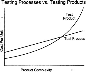
There are two basic approaches to ensuring a high-quality electronic product. First, a manufacturer can design and build products correctly the first time, monitoring processes at every step. This technique, popular with managers because it saves both time and money, includes design verification, extensive process and product simulation, and statistical process control. The alternative is to build the product, test it, and repair it. As Figure 18.2 shows, test-and-repair is more cost effective for simpler products, but its cost increases with product complexity faster than testing the process does. At some point, process testing becomes less expensive. The exact crossover point varies from product to product and from manufacturer to manufacturer.
Figure 18.2. Test-and-repair is cost effective for simple products, but its cost increases with product complexity faster than testing the process does.
Most companies today follow a strategy that falls somewhere between the two extremes. Relying heavily on product test does not preclude being aware of process problems, such as bad solder joints or vendor parts. Similarly, products from even the most strictly controlled process require some testing to ensure that the process remains in control and that no random problems get through the monitoring steps.
Electronics manufacturers select test strategies that include one or more of the techniques listed in Figure 18.3. The following subsections will explore each test technique in detail.
Figure 18.3. Electronics manufacturers select test strategies that include one or more of these test techniques.
18.3.1. Analog Measurements
Bed-of-nails-based automatic test equipment generally performs analog measurements using one or both of the operational-amplifier configurations shown in Figures 18.4 and 18.5.
Figure 18.4. The “apply voltage, measure current” in-circuit measurement technique.
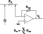
Figure 18.5. The “apply current, measure voltage” in-circuit measurement configuration.
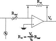
In each case, the operational amplifier, a high-gain difference device featuring high-impedance inputs and a low-impedance output, serves as a current-to-voltage converter. Both versions tie the positive input to ground. Because (ideal) op-amp design requires that the two inputs be at the same potential, the amplifier is stable only when the negative input is at virtual ground and no current flows at that point. Therefore, the current through the two resistors must be identical, and the value of the unknown resistor is proportional to the value of the output voltage Vo.
In Figure 18.4, the measurement injects a known voltage VS. Measuring the current through RRef in the feedback loop determines the unknown resistance RM. This version is often called apply voltage, measure current. In Figure 18.5, the position of the two resistors is reversed, so that the applied current is known. Again, the value of the unknown resistor depends on the ratio of the output voltage to VS, but the factor is inverted. An AC voltage source allows this technique to measure capacitances and inductances.
18.3.2. Shorts-and-Opens Testers
The simplest application of the analog measurement technique is to identify unwanted shorts and opens on either bare or loaded boards. Shorts-and-opens testers gain access to board nodes through a bed of nails. A coarse measurement determines the resistance between two nodes that should not be connected, calling anything less than some small value a short. Similarly, for two points that should connect, any resistance higher than some small value constitutes an open.
Some shorts-and-opens testers handle only one threshold at a time, so that crossover from a short to an open occurs at a single point. Other testers permit two crossovers, so that a short is anything less than, say, 10Ω, but flagging two points as open might require a resistance greater than 50Ω. This “dual-threshold” capability prevents a tester from identifying two points connected by a low-resistance component as shorted.
In addition, crossover thresholds are generally adjustable. By setting open thresholds high enough, a test can detect the presence of a resistor or diode, although not its precise value.
Purchase prices for these testers are quite low, generally less than $50,000. Testing is fast and accurate within the limits of their mission. Also, test-program generation usually means “merely” learning correct responses from a good board. Therefore, board manufacturers can position these testers to prescreen more expensive and more difficult-to-program in-circuit and functional machines.
Unfortunately, the convenience of self-learn programming depends on the availability of that “good” board early enough in the design/production cycle to permit fixture construction. Therefore, manufacturers often create both fixture drill tapes and test programs simultaneously from computer-aided engineering (CAE) information.
Shorts-and-opens testers, as the name implies, directly detect only shorts and opens. Other approaches, such as manufacturing-defects analyzers, can find many more kinds of failures at only marginally higher cost and greater programming effort. Also, the surface-mount technology on today's boards makes opens much more difficult to identify than shorts. As a result, shorts-and-opens testers have fallen into disfavor for loaded boards (bare-board manufacturers still use them), having been replaced by inspection and more sophisticated test alternatives.
In addition, as with all bed-of-nails testers, the fixture itself represents a disadvantage. Beds of nails are expensive and difficult to maintain and require mechanically mature board designs. (Mechanically mature means that component sizes and node locations are fairly stable.) They diagnose faults only from nail to nail, rather than from test node to test node. Sections 18.3.5 and 18.3.6 explore fixture issues in more detail.
18.3.3. Manufacturing-Defects Analyzers
Like shorts-and-opens testers, manufacturing-defects analyzers (MDAs) can perform gross resistance measurements on bare and loaded boards using the op-amp arrangement shown in Figures 18.4 and 18.5. MDAs actually calculate resistance and impedance values and can therefore identify many problems that shorts-and-opens testers cannot find. Actual measurement results, however, may not conform to designer specifications, because of surrounding-circuitry effects.
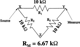
Consider, for example, the resistor triangle in Figure 18.6. Classical calculations for the equivalent resistance in a parallel network,
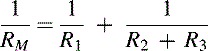 produce a measured resistance of 6.67 kΩ. Like shorts-and-opens testers, MDAs can learn test programs from a known-good board,
so 6.67 kΩ would be the expected-value nominal for this test, despite the fact that R1 is actually a 10-kΩ device.
produce a measured resistance of 6.67 kΩ. Like shorts-and-opens testers, MDAs can learn test programs from a known-good board,
so 6.67 kΩ would be the expected-value nominal for this test, despite the fact that R1 is actually a 10-kΩ device.
Figure 18.6. In this classic resistor triangle, a measured value of 6.67 kΩ is correct, despite the fact that R1 is a 10-kΩ device.
An MDA tester might not notice when a resistor is slightly out of tolerance, but a wrong-valued part, such as a 1-kΩ resistor or a 1-MΩ resistor, will fail. Creating an MDA test program from CAE information can actually be more difficult than for some more complex tester types, because program-generation software must consider surrounding circuitry when calculating expected measurement results.
By measuring voltages, currents, and resistances, MDAs can find a host of failures other than gross analog-component problems. A backwards diode, for example, would fail the test, because its reverse leakage would read as forward drop. Resistance measurements detect missing analog or digital components, and voltage measurements find many backwards ICs. In manufacturing operations where such process problems represent the bulk of board failures and where access is available through board nodes, an MDA can identify 80% or more of all faults.
Like shorts-and-opens testers, MDAs are fairly inexpensive, generally costing less than $100,000 and often much less. Tests are fast, and self-learn programming minimizes test-programming efforts. Because they provide better fault coverage than shorts-and-opens testers, MDAs serve even better as prescreeners for in-circuit, functional, or “hot-mockup” testing.
Again, these testers suffer because of the bed of nails. Contributions from adjacent components severely limit analog accuracy, and there is no real digital-test capability.
18.3.4. In-Circuit Testers
In-circuit testers represent the ultimate in bed-of-nails capability. These sophisticated machines attempt to measure each analog component to its own specifications regardless of surrounding circuitry. Its methods also permit verifying onboard function of individual digital components.
Consider the resistor network in Figure 18.6 if the tester grounds node Z before measuring R1, as Figure 18.7 shows. Theoretically, no current flows through resistor R2 or resistor R3. Therefore, RM = R1 = 10 kΩ. This process of grounding strategic points in the circuit during testing is called guarding, and node Z is known as a guard point.
Figure 18.7. Consider the resistor network in Figure 18.6 if the tester grounds node Z before measuring R1. Theoretically, no current flows through resistor R2 or resistor R3.
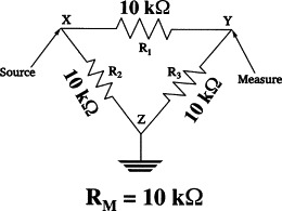
In practice, because the measurement-op-amp's input impedance is not infinite and output impedance is not zero, a small current flows through the guard path. The ratio of measurement-circuit current to guard-path current is known as the guard ratio. A simple three-wire in-circuit measurement, as in Figure 18.7, can achieve guard ratios up to about 100.
For high-accuracy situations and in complex circuits requiring several guard points, assuming that guard-path current is negligible can present a significant problem. Therefore, in-circuit-tester manufacturers introduced a four-wire version, where a guard-point sense wire helps compensate for its current. This arrangement can increase guard ratios by an order of magnitude.
Today, more common six-wire systems address lead resistance in source and measure wires as well. Two additional sense wires add another order of magnitude to guard ratios. This extra accuracy raises tester and fixture costs (naturally) and reduces test flexibility.
Measuring capacitors accurately requires one of two approaches. Both involve measuring voltage across a charged device. In one case, the tester waits for the capacitor to charge completely, measures voltage, and computes a capacitance. For large-value devices, these “settling times” can slow testing considerably. Alternately, the tester measures voltage changes across the device as it charges and extrapolates to the final value. Although more complex, this technique can significantly reduce test times.
In-circuit-tester manufacturers generally provide a library of analog device models. A standard diode test, for example, would contain forward-voltage-drop and reverse-current-leakage measurements. Program-generation software picks tests for actual board components, assigning nominal values and tolerances depending on designers' or manufacturing-engineers' specifications. Analog ICs, especially custom analog ICs, suffer from the same lack of automated programming tools as their complex digital counterparts.
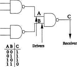
Digital in-circuit testing follows the same philosophy of isolating the device under test from others in the circuit. In this case, the tester injects a pattern of current signals at a component's inputs that are large enough to override any preexisting logic state, then reads the output pattern. Figure 18.8 shows an in-circuit configuration for testing a two-input NAND gate.
Figure 18.8. An in-circuit configuration for testing a two-input NAND gate.
For combinational designs, the in-circuit approach works fairly well. Output states are reasonably stable. Good boards pass, bad boards fail, and test results generally indict faulty components accurately.
Sequential circuits, however, present more of a problem. Consider the simple flip-flop in Figure 18.9.
Figure 18.9. A noise glitch that escapes from NAND-gate B may look like another clock signal to the flip-flop.
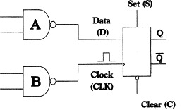
Most tests assert a state on the D line, clock it through, then hold the D in the opposite state while measuring the outputs. A noise glitch that escapes from NAND-gate B may look like another clock signal to the flip-flop. If D is already in the “wrong” state, the outputs will flip and the device will fail. A similar problem may occur from glitches on SET or CLEAR lines.
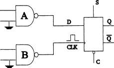
To alleviate this problem, the in-circuit tester can ground one input on each gate at the flip-flop input, as in Figure 18.10, guaranteeing that their outputs (and therefore the inputs to the device under test) remain at 1. This extra step, called digital guarding, minimizes the likelihood that any glitches will get through. For standard-voltage devices (TTL, CMOS), an in-circuit tester can overdrive a one to a zero more easily than a zero to a one, so digital guarding ensures that test-device inputs are all at 1, if possible. For ECL technologies, because of their “high ground,” guarding software places device inputs at 0 before testing.
Figure 18.10. Grounding one input on each gate at the flip-flop input in Figure 18.9.
Test and CAE equipment vendors offer test routines for simple “jellybean” digital devices, such as gates, counters, and flip-flops, as well as cursory tests for fairly complex devices, such as microprocessors. Constructing in-circuit test programs for boards whose designs consist primarily of those devices requires merely “knitting” individual device tests together, based on interconnect architecture, and generating analog and digital guard points where necessary.
Many of today's complex boards require a large number of bed-of-nails access pins, sometimes as many as several thousand. Because only a relative handful must be active at any time during testing, tester vendors can minimize the number of actual pin drivers and receivers through a technique known as multiplexing. With multiplexing, each real tester pin switches through a matrix to address one of several board nodes. The number represents the multiplex ratio. An 8:1 multiplex ratio, for example, means that one tester pin can contact any of eight pins on the board.
The technique reduces in-circuit-tester costs while maximizing the number of accessible board nodes. On the other hand, it introduces a switching step during test execution that can increase test times. In addition (and perhaps more important), it significantly complicates the twin tasks of test-program generation and fixture construction, because for any test, input and output nodes must be on different pins. Aside from simple logistics, accommodation may require much longer fixture wires than with dedicated-pin alternatives, which can compromise test quality and signal integrity.
Most in-circuit testers today employ multiplexing. To cope, many test-program generators assign pins automatically, producing a fixture wiring plan along with the program. Waiting for that information, however, can lengthen project schedules. Revising a fixture to accommodate the frequent changes in board design or layout that often occur late in a development cycle may also prove very difficult. Nevertheless, if the board contains 3000 nodes, a dedicated-pin solution may be prohibitively expensive or unavailable.
In-circuit testers offer numerous advantages. Prices between about $100,000 and $300,000 are generally lower than for high-end functional and some inspection alternatives, and they are generally less expensive to program than functional testers. Test times are fast, and although functional testers feature faster test times for good boards, bad-board test and fault-diagnostic times for in-circuit testers can be substantially lower. In-circuit testers can often verify that even complex boards have been built correctly.
At the same time, however, three forces are combining to make test generation more difficult. First, flip chips, BGAs, and other surface-mount and hidden node varieties often severely limit bed-of-nails access. In addition, the explosion of very complex devices increases the burden on tester and CAE vendors to create device-test programs. These tests are not identical to tests that verify device-design correctness.
Also, as electronic products become both smaller and more complex, hardware designers increasingly rely on ASICs and other custom solutions. Test programs for these parts must be created by device designers, board designers, or test engineers. Because ASIC production runs are orders of magnitude lower than production runs for mass-marketed devices such as microprocessors and memory modules, much less time and money are available for test-program creation. Complicating the problem, device designers often do not have final ASIC versions until very near the release date for the target board or system. Therefore, pressure to complete test programs in time to support preproduction and early production stages means that programs are often incomplete.
Perhaps the biggest drawback to in-circuit test is that it provides no assessment of board performance. Other disadvantages include speed limitations inherent in bed-of-nails technology. Nails add capacitance to boards under test. In-circuit test speeds even approaching speeds of today's lightning-fast technologies may seriously distort stimulus and response signals, as square waves take on distinctly rounded edges.
Traditionally, long distances between tester drivers and receivers often cause problems as well, especially for digital testing. Impedance mismatches between signals in the measurement path can cause racing problems, reflections, ringing, and inappropriate triggering of sequential devices. Fortunately, newer testers pay much more attention to the architecture's drawbacks by drastically limiting wire lengths, often to as little as 1 in.
Board designers dislike the technique because it generally requires a test point on every board node to allow device access. Overdriving some digital device technologies can demand currents approaching 1A! Obtaining such levels from an in-circuit tester is difficult at best. In addition, designers express concern that overdriving components will damage them or at least shorten their useful lives. Therefore, many manufacturers are opting to forego full in-circuit test, preferring to use an MDA or some form of inspection to find manufacturing problems and then proceeding directly to functional test.
One recent development is actually making in-circuit testing easier. As designers integrate more and more functionality onto single devices, real-estate density on some boards is declining.
For example, shrinking boards for desktop computers, telephone switching systems, and similar products realizes few advantages. Even notebook computers cannot shrink beyond a convenient size for keyboard and display. A few years ago, IBM experimented briefly with a smaller-than-normal form factor notebook computer. When the user opened the lid, the keyboard unfolded to conventional size. Unfortunately, reliability problems with the keyboard's mechanical function forced the company to abandon the technology. (Although some palmtop computers feature a foldable keyboard design, their keyboards are much smaller than those of a conventional PC, making the mechanical operation of the folding mechanism considerably simpler.) Since that time, minimum x-y dimensions for notebook computers have remained relatively constant, although manufacturers still try to minimize the z-dimension (profile). In fact, some new models have grown larger than their predecessors to accommodate large displays.
Two recent disk-drive generations from one major manufacturer provide another case in point. The earlier-generation board contained hundreds of tiny surface-mounted components on both sides. The later design, which achieved a fourfold capacity increase, featured half a dozen large devices, a few resistor packs, bypass capacitors, and other simple parts, all on one side. Boards destined for such products may include sufficient real estate to accommodate through-hole components, test nodes, and other conveniences.
In-circuit testing of individual devices, however, has become more difficult, especially in applications such as disk-drive test that contain both analog and digital circuitry. At least one in-circuit tester manufacturer permits triggering analog measurements “on the fly” during a digital burst, then reading results after the burst is complete. This “analog functional-test module” includes a sampling DC voltmeter, AC voltmeter, AC voltage source, frequency- and time-measurement instrument, and high-frequency multiplexer.
Consider, for example, testing a hard-disk-drive spindle-motor controller such as the TA14674 three-phase motor driver with brake shown in Figure 18.11. This device offers three distinct output levels—a HIGH at 10V, LOW at 1.3V, and OFF at 6V. Durickas (1992) suggests that, although a CMOS logic-level test will verify basic functionality, accurately measuring the voltages themselves increases test comprehensiveness and overall product quality.
Figure 18.11. A TA14674 three-phase hard-disk-drive spindle-motor controller with brake
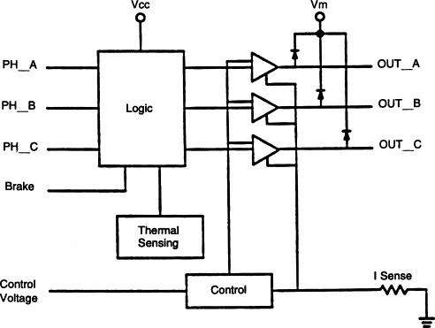
(From Durickas, 1992).
To conduct such a test, Durickas requires prior testing of certain passive components that surround the controller, then using those components to set important operating parameters for the primary device test. Therefore, his approach necessitates bypassing the controller test if any of the passive components fails.
The main test consists of four steps. The first provides all valid and invalid logic input states and measures digital outputs at CMOS logic levels—VOH = 9.5V, VOL = 1.75V. A pass initiates three additional tests, one for each output. Each output test requires six analog voltage measurements, as Figure 18.12 shows. This hybrid test capability minimizes the number of boards that pass in-circuit test only to fall out at the next test station, in this case usually a hot mockup.
Figure 18.12. An in-circuit test for the component in Figure 18.11. Testing each output requires six analog voltage measurements
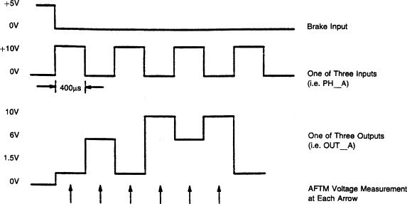
(From Durickas, 1992).
18.3.5. Bed-of-Nails Fixtures
As indicated earlier, beds-of-nails represent a disadvantage for any test method that must employ them. Nevertheless, the technique can be the only solution to a test problem.
All bed-of-nails fixtures conform to the same basic design. At the base of each fixture is a receiver plate, which brings signals to and from the tester, usually on a 100-mil (0.100-in.) grid. Wires connect appropriate receiver pins to spring-loaded probes that contact the board under test through a platen that is drilled to precisely match the board's electrical nodes and other test points. Each receiver pin corresponds to one and only one board node.
Vacuum or mechanical force pulls the board under test down onto the fixture, pushing the probes out through the platen to make contact. Spring-probe compression exerts about 4 to 8 oz. of force at the test point, ensuring a clean electrical connection.
Some fixtures forego the “rat's nest” of wires from receiver to probes in favor of a printed-circuit board. This choice improves speed and reliability while minimizing crosstalk and other types of interference. Such “wireless fixtures” are less flexible than their more traditional counterparts. In addition, lead times to manufacture the circuit board may make delivering the fixture in time to meet early production targets more difficult.
There are four basic types of bed-of-nails fixtures. A conventional, or dedicated, fixture generally permits testing only one board type, although a large fixture sometimes accommodates several related small boards.
A universal fixture includes enough pins on a standard grid to accommodate an entire family of boards. The specific board under test rests on a “personality plate” that masks some pins and passes others. Universal fixtures generally cost two to three times as much as their conventional counterparts. Pins also require more frequent replacement because although testing a particular board may involve only some pins, all pins are being compressed. Therefore, if a pin permits 1 million repetitions, that number must include occasions where the pin merely pushes against the bottom of the personality plate. The high pin population on universal fixtures makes troubleshooting faulty pins and other maintenance much more difficult than in the conventional type.
Surface-mount fixtures also attach to a standard 100-mil receiver grid. In this case, however, a series of translator pins pass through a center fixture platen so that at the board, the pins can be much closer together, as Figure 18.13 shows. The principle here is that, even on heavily surface-mount boards, not all nodes require very close centers. The center platen minimizes pin bending and therefore improves pointing accuracy.
Figure 18.13. In surface-mount fixtures, a series of translator pins pass through a center fixture platen so that at the board the pins can be much closer together.
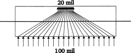
This type of fixture is about 20 to 50% more expensive than a conventional type. In addition, if too many areas on the board contain close centers, the number of available tester pins may be insufficient, or wires from the receiver may be too long to permit reliable testing.
Each of these fixture designs assumes that the tester requires access to only one board side at a time. This approach means either that all test nodes reside on one side (usually the “solder” side) or that board design permits dividing the test into independent sections for each side. This latter approach, of course, means that each board requires two fixtures and two tests. In many manufacturing operations, however, capacity is not at issue, so that testing boards twice per pass does not present a problem.
Testing both board sides simultaneously requires a clamshell fixture that contains two sets of probes and closes onto the board like a waffle iron. Clamshell fixtures are extremely expensive. A test engineer from a large computer company reported that one of his fixtures cost nearly $100,000. To be fair, the board was 18" × 18" and contained several thousand nodes. Nevertheless, fixture costs that approach or exceed tester costs may necessitate seeking another answer.
Clamshell-fixture wires also tend to be much longer than wires on a conventional fixture. Wire lengths from the receiver to the top and bottom pins may be very different, so that signal speeds do not match. If a pin or wire breaks, finding and fixing it can present quite a challenge. The rat's nest in one of these fixtures makes its conventional counterpart look friendly by comparison.
The accuracy, repeatability, and reliability of a clamshell fixture's top side are poorer than those of a conventional solution. Access to nodes and components on the board for probing or pot adjustment is generally impossible. In addition, the top side of a clamshell fixture often contacts component legs directly. Pressure from nails may make an electrical connection when none really exists on the board, so the test may not notice broken or cold-solder joints.
Although clamshell fixtures present serious drawbacks, they often provide the only viable way to access a board for in-circuit or MDA test. Because of their complexity, they bring to mind a dog walking on its hind legs: It does not do the job very well, but considering the circumstances, you have to be amazed that it can do the job at all.
Bed-of-nails fixtures permit testing only from nail to nail, not necessarily from node to node. Consider a small-outline IC (SOIC) or other surface-mounted digital component. Actual electrical nodes may be too small for access. For BGAs and flip chips, nodes reside underneath. In any case, pads are often some distance from the actual component under test. Therefore, a trace fault between the component and the test pad will show up as a component fault, whereas the continuity test between that pad and the next component or pad will pass.
Service groups rarely use bed-of-nails systems. Fixtures are expensive and difficult to maintain at correct revision levels when boards returning from the field may come from various product versions, some of which the factory may not even make anymore. Necessary fixture storage space for the number of board types handled by a service depot would generally be excessive.
Alternatives include foregoing the factory bed-of-nails test altogether to permit a common test strategy in the factory and the field. Some vendors offer service testers that can mimic the behavior of their bed-of-nails products without the need for conventional fixtures. Operation involves scanners, x-y probers, or clips and probes. These testers can be less expensive than their factory-bound counterparts. Software and test programs are compatible or can be converted between the two machine types.
18.3.6. Bed-of-Nails Probe Considerations
Figure 18.14 shows a typical bed-of-nails probe construction, including a plunger, barrel, and spring. This design allows variations in target height. Spring-probe tips must pierce board-surface contamination to permit a low-resistance connection. Therefore, probe manufacturers provide a plethora of tip styles for different applications. Figure 18.15 presents some common types. To avoid the confusion of including several tip styles on a single fixture, test engineers usually choose one that provides the best compromise for a particular board.
Figure 18.14. Construction for a typical bed-of-nails probe (Interconnect Devices, Kansas City, KA).
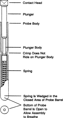
Figure 18.15. A selection of available probe tip styles (Interconnect Devices, Kansas City, KS).
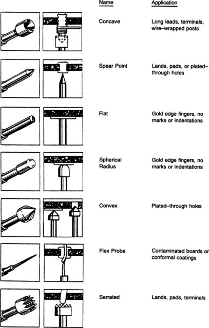
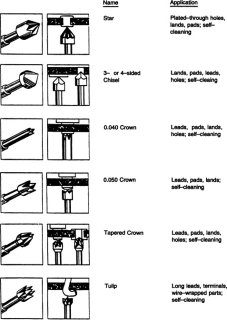
Chisel tips easily penetrate oxide contamination on solder pads and plated-through holes, the most common targets. Other solutions include stars, tulips, and tapered crowns. These tips are self-cleaning, meaning that each probe cycle wipes away flux residue, solder resist, and other contaminants, increasing test accuracy and extending probe life. Many board manufacturers, especially in Japan, choose star tips for plated-through-hole applications, such as bare-board testing. Penetrating an oxide layer with a star tip requires higher spring force than with other designs, but the star provides more contact points.
Other probe tips offer advantages, as well. Concave tips accommodate long leads and wire-wrap posts. A tendency to accumulate debris, however, makes these tips most effective in a “pins down” position.
Spear tips, which are usually self-cleaning unless they contain a flat spot or large radius, can pierce through surface films on solder pads. As a general solution, however, Mawby (1989) cautions against probing holes larger than half the diameter of the spear-tip plunger.
Flat tips and spherical-radius tips work well with gold-plated (and therefore uncorroded) card-edge fingers. Convex designs apply to flat terminals, buses, and other solid-node types. These tips are not self-cleaning when probing vias.
Flex tips can pierce conformal coatings, as on many military boards. Of course, these boards require recoating after test. Serrated tips work well for access to translator pins or on terminal strips that contain some surface contamination.
Success for a particular tip style depends on both its geometry and the accompanying spring force. Too little force may prevent good electrical contact. Too high a force may damage delicate board pads and other features.
Some probes rotate as they compress. This action helps the probe to pierce through conformal coatings, corrosion, and other surface contamination to ensure good contact.
Test engineers must carefully distribute pins across a board's surface to avoid uneven pressure during testing. Such pressure can cause bending moments, reducing the pointing accuracy of pins near the board edge and possibly breaking solder bonds or tombstoning surface-mounted components.
Ensuring high-quality circuit resistance measurements and digital tests requires low interface resistance and good node-to-node isolation. According to Mawby, fixture-loop resistance—including switching circuitry, wires, and probes—ranges between 1Ω and 5Ω. Although its magnitude is not much of an impediment for shorts and opens and other self-learned tests that compensate for it automatically, node-to-node variations must remain much less than shorts-and-opens thresholds. In-circuit testers must subtract out this so-called tare resistance to achieve necessary measurement accuracies.
A low contact resistance, usually specified as less than 500 mΩ, also ensures maximum test speed and accuracy. Contact resistances tend to increase as probes age, however, primarily from corrosion and other contamination. Cleaning helps minimize the problem but cannot eliminate it completely.
Pointing accuracy specifies how closely a pin can hit its target. Repeatability indicates the consistency from cycle to cycle. Keller and Cook (1985) estimated an accuracy (1 standard deviation, or 1 σ) of ±4 mils for 100-mil probes and ±5 mils for 50-mil probes. Of course, if pins bend as they age, these figures will get worse. The researchers recommend surface-mount-board test pads with diameters of 3 σ or 4 σ. At 3 σ, approximately 3 probes in 1000 would miss their targets. At 4 σ, less than 1 in 10,000 would miss. Based on these numbers, 100-mil probe pads should be 24 mils or 32 mils in diameter, and 50-mil pads should be 30 mils or 40 mils. Designers may justifiably balk at consuming so much real estate “merely” for test pads.
Mawby refers to new probe designs that achieve accuracies of ±1.5 mils for 50-mil surface-mount boards. These probes need test pads only 9 mils or 12 mils in diameter to meet 3-σ and 4-σ requirements. St. Onge (1993) also explores hitting small targets with a conventional bed of nails.
Unfortunately, probes do not last forever. Standard models are rated for about 1 million cycles if there is no side loading. Probe life is approximately proportional to cross-sectional area. Therefore, if a 50-mil-pin barrel diameter is half of the barrel diameter for a 100-mil pin, it will likely last only one quarter as long. Because pin replacement is a maintenance headache, this shortened life constitutes a major concern. Some probe manufacturers have introduced small-center models with larger-than-normal barrel diameters specifically to address the life issue. Although they do not last as long as their 100-mil siblings, these models can last twice as long as other small-center designs. To hit targets smaller than 50 mils, some probes adopt the traditional design but completely eliminate the receptacle, mounting directly to thin mounting plates. Because small pins are more fragile and can be less accurate, a test fixture should include 100-mil pins wherever possible, resorting to 50-mil and smaller ones only where necessary.
18.3.7. Opens Testing
As stated earlier, the proliferation of surface-mount technologies has aggravated the problem of opens detection to the point where it is now often the most difficult manufacturing fault to detect. Some such problems defy electrical testing altogether and encourage some kind of inspection.
Techniques have emerged to detect many opens—assuming (and this assumption is becoming ever more of a constraint) that you have bed-of-nails access to the board nodes. They perform measurements on unpowered boards and often rely on clamp diodes that reside inside the IC between I/O pins and ground or on “parasitic diodes” formed by the junction between the pin and the substrate silicon.
The common techniques can be broadly divided into two groups. Parametric process testing measures voltage or current on the diodes directly or by forming them into transistors. This approach requires no special hardware beyond the fixture itself.
The simplest version applies voltage to the diode through the bed of nails, then measures the current. An open circuit generates no current and no forward voltage. Unfortunately, this method will miss faults on parallel paths.
One variation biases the diode input (emitter) and output (collector) relative to ground, then compares collector current on groups of pins. Proponents contend that this approach proves less sensitive to device/vendor differences than the more conventional alternative. It can detect opens right to the failing pin, as well as misoriented devices and incorrect device types. It will sometimes identify a device from the wrong logic family and may find resistive joints and static damage, depending on their severity.
On the downside, program debugging for this method requires “walking around” a reference board and opening solder joints. It also may not see differences between simple devices with the same pinouts but different functions. It cannot detect faults on power or ground buses, but that limitation is also true with the other techniques.
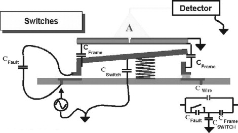
In capacitive testing, a spring-mounted metal plate on top of the IC package forms one side of a capacitor. The IC lead frame forms the other side, with the package material the dielectric. The tester applies an AC signal sequentially to the device pins through the bed of nails. The probe-assembly buffer senses the current or the voltage to determine the capacitance. In this case, the measurement circuits see only the pins, not the bond wire and internal diodes, detecting only opens between the IC pins and the board surface. It can, therefore, examine the connectivity of mechanical devices such as connectors and sockets, as well as ICs. Because of the extra hardware required, this technique increases bed-of-nails fixture costs.
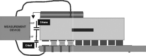
Figure 18.16 shows the capacitor formed by an open IC circuit. The lead frame forms one plate, the pad and trace on the PCB the other. The lack of solder in between (air) forms the dielectric, creating a capacitor of about 25 fF. The measurement system places a conductor over the lead frame, as in Figure 18.17, forming an additional capacitor of about 100 fF. An open circuit would produce these two capacitances in series, for an equivalent capacitance of 20 fF. In a good joint, the measurement would see only the 100-fF test capacitor.
Figure 18.16. Anatomy of an open-solder capacitor (Agilent Technologies).
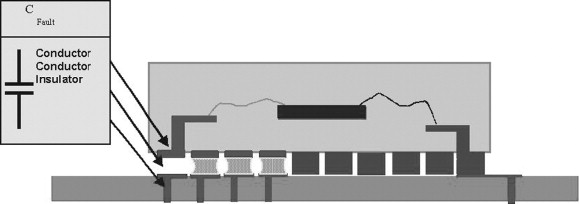
Figure 18.17. The measurement system places a conductor over the lead frame, forming an additional capacitor of about 100 fF (Agilent Technologies).
This theory also applies to testing other components with internal conductors, such as connectors and sockets, as Figure 18.18 shows. Testing sockets ensures proper operation before loading expensive ICs onto the board at the end of the assembly process. The measurement system grounds pins in the vicinity of the pin under test. The resulting capacitance is often higher than for an IC, which may cause the capacitance of a solder open to be higher as well. Figure 18.19 shows the same principle applied to a switch.
Figure 18.18. Measuring opens in connectors and sockets (Agilent Technologies).
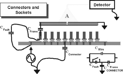
Figure 18.19. Applying the same principle to a switch (Agilent Technologies).
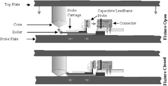
You can probe even right-angle connectors using this technique. In that case, however, you do have to create a bit of custom fixturing. Figure 18.20 shows one possibility. The capacitive lead frame is mounted on a sliding mechanism called a probe carriage. The spring-loaded probe carriage retracts the lead-frame probe when the fixture is open, to allow the operator to more easily load and unload the board under test. In the closed fixture, the cone pushes on a roller bearing that is part of the carriage, moving it and the lead-frame probe to the connector.
Figure 18.20. Custom fixturing for testing a right-angle connector (Agilent Technologies).
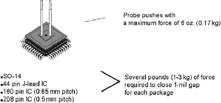
Some manufacturers have expressed concern that the force of the capacitive probe will close the solder gap, creating a connection where none really exists. As Figure 18.21 shows, the force exerted is far less than would be required to do this.
Figure 18.21. The force of the probe is far less than that necessary to close the solder gap.
18.3.8. Other Access Issues
With bed-of-nails access becoming more difficult, companies often rely more on functional or cluster testing to verify digital circuitry. Because analog circuits do not lend themselves easily to that approach, it has become necessary to find a viable alternative. With an average of two to three analog components on every board node, every node that defies probing reduces the number of testable components by that same two or three. Pads have shrunk to only a few mils, and center-to-center probe distances have fallen as well. So-called no-clean processes require higher probing forces to pierce any contaminants on the node, which increases stress on the board during bed-of-nails test. In fact, 2800 124-oz. probes exert a ton of force. Clearly, less access may occur even where nodes are theoretically available.
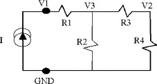
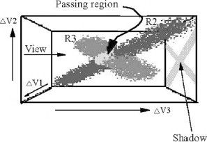
McDermid (1998) proposes a technique for maximizing test diagnostics with as little as 50% nodal access. He begins with an unpowered measurement, using a small stimulus voltage to break the circuit into smaller pieces. In this situation, device impedances are sufficient to appear to the tester as open circuits. Clusters of analog components are connected by either zero or one node. Typically, these clusters are small and isolated from one another. We assume no more than one failing node per cluster.
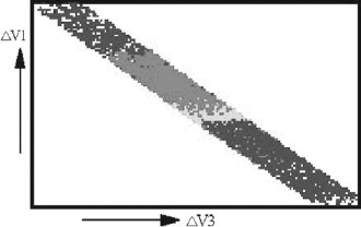
Consider the circuit in Figure 18.22. I is the system stimulus. When circuit components are at nominal values, the voltages are defined as nominal as well. Varying component values within tolerance limits produces voltages that fall into a scatter diagram, such as the one in Figure 18.23. If R1 or R3 fail, the scatter diagram looks like the one in Figure 18.24. If nodes are available for only V1 and V2, you see the two-dimensional shadow depicted, and shown in more detail in Figure 18.25. If only V1 and V3 permit access, the shadow looks like Figure 18.26. In this view, you cannot tell which resistor has failed, demonstrating the importance of selecting test points carefully. Figure 18.27 presents actual results from this technique.
Figure 18.22. Circuit diagram for the limited-access example
(From McDermid, 1998; Agilent Technologies).
Figure 18.23. Varying component values within tolerance limits produces voltages that fall into a scatter diagram
(From McDermid, 1998; Agilent Technologies).
Figure 18.24. The scatter diagram if R1 or R3 fails
(From McDermid, 1998; Agilent Technologies).
Figure 18.25. Looking at the scatter-diagram “shadow” if nodes are available only on V1 and V2
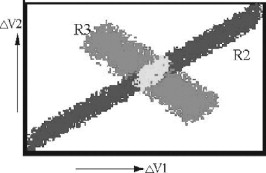
(From McDermid, 1998; Agilent Technologies).
Figure 18.26. The shadow with nodes only on V1 and V3
(From McDermid, 1998; Agilent Technologies).
Figure 18.27. Actual test results with limited access
(From McDermid, 1998; Agilent Technologies).
18.3.9. Functional Testers
Functional testers exercise the board, as a whole or in sections, through its edge connector or a test connector. The tester applies a signal pattern that resembles the board's normal operation, then examines output pins to ensure a valid response. Draye (1992) refers to this type of test as “general-purpose digital input/output measurement and stimulus.” Analog capability generally consists of a range of instruments that provide analog stimuli or measurements in concert with the board's digital operation.
Some complex boards also require a “modified” bed of nails to supplement edge and test connectors. Differences between in-circuit and functional beds of nails include the number of nails and their purpose. Whereas an in-circuit bed of nails provides a nail for every circuit node, functional versions include nails only at critical nodes that defy observation from the edge connector. Relying on only a few nails avoids loading the circuit with excess capacitance, which would reduce maximum reliable test speeds.
A functional-test bed of nails cannot inject signals. It provides observation points only. Reducing functional-test logic depth, however, simplifies test-program generation considerably.
Functional beds of nails remain unpopular with most board manufacturers because of fixture costs, scheduling pressures, and nail capacitances. These concerns have spurred the growth of boundary-scan designs (see Chapter 19) as an alternative for internal-logic access.
An MDA or an in-circuit test measures the success of the manufacturing process. Functional testing verifies board performance, mimicking its behavior in the target system. Because this test tactic addresses the circuit's overall function, it can apply equally well to testing large circuit modules or hybrids and to system testing.
Functional test can occur at full speed, thereby uncovering racing and other signal-contention problems that escape static or slower-speed tests. This test also verifies the design itself, as well as how well the design has translated to the real world. Test times for passing boards are the fastest of any available technique, and failure analysis can indicate the correct fault, almost regardless of board real-estate population density.
Functional test is traditionally the most expensive technique. Also, automatic functional testing is still basically a digital phenomenon. Programming is difficult and expensive and traditionally involves a complex cycle of automatic and manual steps. Analog automatic program generation is nearly nonexistent.
Most functional testers work best at determining whether a board is good or bad. Pinpointing the cause of a failure can take much longer than the test itself. Diagnostic times of hours are not unheard of. Many companies have “bone piles” of boards that have failed functional test, but where the cause remains unknown.
A bed-of-nails tester can identify all failures from a particular category (shorts, analog, digital) in one test pass. For a functional test, any failure requires repair before the test can proceed. Therefore, a test strategy that eliminates bed-of-nails techniques must achieve a very high first-pass yield with rarely more than one fault per board to avoid multiple functional-test cycles.
Solutions that address these issues are emerging. Some new benchtop functional testers are much less expensive than their larger siblings. A traditional functional tester can cost hundreds of thousands of dollars, whereas benchtop prices begin at less than $100,000. Larger testers still perform better in applications requiring high throughput and very high yields, but for many manufacturers, small functional testers can offer a cost-effective alternative.
18.3.10. Functional Tester Architectures
Digital functional testing comes in several forms. Differences involve one or more of certain test parameters:
- Test patterns Logical sequences used to test the board
- Timing Determines when the tester should drive, when it should receive, and how much time should elapse between those two events
- Levels Voltage and current values assigned to logic values in the pattern data. Levels may vary over the board, depending on the mix of device technologies.
- Flow control Program tools that specify loops, waits, jumps, and other sequence modifiers
The simplest type of digital functional “tester” is an I/O port. It offers a limited number of I/O channels for a board containing a single logic family. The I/O port offers a low-cost solution for examining a few digital channels. However, it is slow and provides little control over timing or logic levels during test, severely limiting its capability to verify circuits at-speed or to-spec.
Emulators exploit the fact that many digital boards feature bus-structured operation and resemble one another functionally. A somewhat general, hardware-intensive test can verify those common functions, reducing overall test development effort. Emulation replaces a free-running part of the board's logic with a test pod. It then mimics the board's behavior in the target system, stopping at convenient points to examine registers and other hardware states. Figure 18.28 shows a simplified block diagram of a typical emulation tester.
Figure 18.28. A simplified block diagram of a typical emulation tester
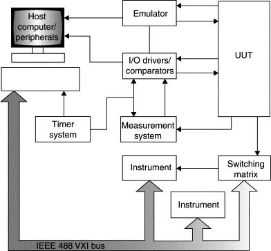
(From Eisler, 1990).
Emulation is perhaps the least well-understood test technique. One problem is that many sources refer to it as in-circuit emulation, yet it has nothing to do with in-circuit testing. Calling it performance testing, as other sources do, better describes its operation.
There are three basic types of emulation. Most familiar is microprocessor emulation, where a test pod attaches to the microprocessor leads or plugs into an empty microprocessor socket. On boards with more than one processor, the test must replace all of them, either serially or simultaneously. A successful test requires that the board's power and clock inputs, reset, data-ready, and nonmaskable interrupts function correctly.
Memory emulation replaces RAM or ROM circuitry on the board under test, then executes a stored program through the existing microprocessor and surrounding logic, including clock, address and data buses, address decoder, and RAM. Because the microprocessor remains part of the circuit, this variation has advantages over microprocessor emulation for production test. Also, the tester does not require a separate pod for each microprocessor, only one for each memory architecture, reducing hardware acquisition and development costs.
Bus-timing emulation does not actually require the presence of a microprocessor on the board at all. It treats the processor as a “black box” that simply communicates with the rest of the board logic over I/O lines. The bus can be on the board or at the edge connector. The technique executes MEMORY READ, MEMORY WRITE, INPUT, OUTPUT, FETCH, and INTERRUPT functions from the processor (wherever it is) to assess board performance.
Bus emulators contain a basic I/O port, but include local memory behind the port for caching digital test patterns as well, giving considerably more control over speed and timing. Emulators offer three types of channels: address field, data field, and timing or control channels. Logic levels are fixed, and the system controls timing within address and data fields as a group, rather than as individual channels. The emulator loads the bus memory at an arbitrary speed, triggers the stimulus at the tester's fixed clock rate, then collects board responses on the fly in response memory. Unloading the memory at a convenient speed provides the test results.
Bus-timing emulation is an ideal technique for testing boards that do not contain microprocessors but are destined for microprocessor-based systems. The classic example is a personal-computer expansion board or a notebook computer's credit-card-sized PCMCIA board. The PC's I/O bus is well defined. The tester latches onto the bus and executes a series of functions that are similar to what the board experiences inside the PC. The test can even include erroneous input signals to check the board's error-detection capabilities. Tools include noise generators, voltage-offset injectors, and similar hardware.
Emulation testers are generally quite inexpensive. In fact, it is possible to execute a bus-emulation test for some products without an actual tester. A conventional PC contains most of the necessary hardware. An expansion board and proper software may suffice to create a “test system.”
Program development may also be less expensive and less time consuming than development for a more-elaborate functional test. A microprocessor emulation test resembles a self-test for he corresponding system. Test engineers can avoid creating a software behavioral model of a complex IC, choosing instead to emulate it with a hardware pod.
Emulation tests boards in their “natural” state. That is, it does not apply every conceivable input combination, restricting the input set to those states that the target product will experience.
Emulation can also find obscure faults by “performance analysis.” It can identify software problems by tracking how long the program executes in each area of memory. In some cases, software contains vestigial routines that do not execute at all. Recent revisions may have supplanted these routines, yet no one has deleted them. They take up memory space, and their mere presence complicates debugging and troubleshooting the software to no purpose. In other cases, a routine should execute but does not.
For example, an unused routine may provide a wait state between two events. Unless the system usually or always fails without that delay, the fact that the software lies idle goes unnoticed. If the emulation test knows to look for program execution in that section of memory and it never gets there, the test will fail. This technique will also notice if the software remains too long in a section of memory or not long enough (such as an n-cycle loop that executes only once).
Emulation permits finding certain failures that are difficult or impossible to detect in any other way. One such example is single-bit-stack creep. A computer system stuffs information into a data stack in bytes or other bit-groups for later retrieval. If noise or some other errant signal adds or deletes one or more bits, all subsequent stack data will violate the specified boundaries, and retrieved data will be garbled. The ability to stop the system to examine hardware registers (such as stacks) will uncover this particularly pernicious problem. As digital-device voltages continue to fall, this kind of fail-safe testing becomes more important.
Disadvantages of this technique include the need for individual emulation modules for each target microprocessor, RAM configuration, or I/O bus. Module availability presents few impediments other than cost if the target configuration is common, such as an ISA or USB PC bus or a Pentium-class microprocessor. Testing custom systems and new designs, however, may have to wait for the pod's completion.
Program generation is nearly always a manual process and requires a programmer with intimate knowledge of circuit behavior. Therefore, test development tends to miss unusual failure mechanisms, because the person most familiar with a board's design is not the person most likely to anticipate an oddball result.
Emulation requires that the target system be microprocessor based. Creating guided-probe diagnostics is both expensive and time consuming, especially for memory and bus-timing variations where the microprocessor is not completely in control of the circuit. The technique offers no significant analog testing and no clear way to isolate faults outside of the kernel logic. In addition, there is no easy way to determine fault coverage accurately, so it is difficult to decide when to stop program development. Many test engineers simply establish a set of test parameters and a timetable. When the time is exhausted, the test program is declared complete.
For finding a failure with a microprocessor-emulation test, consider the flowchart in Figure 18.29. Here, the board's internal self-tests have failed, and the microprocessor has either stopped or is running wild. A passive examination of circuit behavior has produced no diagnosable symptoms.
Figure 18.29. A flowchart for finding a failure with a microprocessor-emulation test
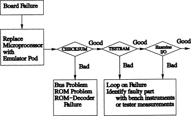
(From Scheiber, 1990).
The test operator replaces the board's microprocessor with an emulator pod or clips the pod onto the processor's I/O pins and executes a CHECKSUM test on the ROMs. This test involves reading all ROM locations, adding them up, and comparing the results to the corresponding numbers stored on the ROMs themselves. If the numbers match, the test moves on. Any difference indicates a problem with one of the ROMs, the ROM bus, or the decoder. On a failure, the tester enters a diagnostic loop, providing a sync pulse that allows examining the circuit with a logic analyzer or other external instrument to pinpoint the faulty component.
If the CHECKSUM test passes, the next step is a TESTRAM that verifies read/write memory devices and their surrounding buses. If this test fails and the buses are presenting legal WRITE and CHIP-SELECT signals, the fault lies in one or more devices. Again, looping at a convenient hardware state allows further analysis with bench instruments. Experience has shown that, with these symptoms, a RAM decoder or driver is a frequent culprit.
If ROMs, RAMs, and their corresponding buses have passed, the test checks the board's I/O. I/O tests can be simple or complex, depending on the situation. Steps include reading A/D converter output values, reading and setting parallel bits, and examining complex devices such as direct-memory-access (DMA) channels. In some cases, obtaining meaningful data from I/O devices can require programming dozens of internal registers. Therefore, many emulation testers offer overlay RAM, which overrides onboard memory during test execution. This approach allows examining board logic, for example by triggering I/O initialization routines, regardless of any memory faults.
Digital word generators resemble the memory-and-state-machine architecture of emulators but provide a more general-purpose solution. Like the emulator, they store stimulus and response signals in local memory. They also include several types of fixed-logic-level channels but add some programmable channels as well. Channels again exist as groups, and the tester can control them only as groups. However, you can add or configure signal channels by buying additional modules from the tester manufacturer. This architecture offers more flexibility than the emulators do. Nevertheless, timing flexibility is similarly limited, and programmable timing and test speed is limited to the time necessary to perform one memory-access cycle.
Most sophisticated in the digital-test arsenal is the performance functional tester. This system tests the board operation to established specifications, rather than “merely” controlling it. The tester can emulate the board-to-system interface as closely as possible to ensure that the board will work in the final system without actually installing it.
This alternative offers highly flexible digital channels, as well as individually selectable logic levels (to serve several logic families on the same board), timing, and control. To synchronize the test with analog measurements, the tester often includes special circuitry for that purpose. Subject to the tester's own specifications, it can precisely place each signal edge. Programs are divided into clock cycles, rather than events, permitting more direct program development through interface with digital simulators.
Conventional stimulus/response functional testing relies on simulation for test-program development. As boards become more complex, however, programmers must trade off test comprehensiveness against simulation time. Design or test engineers who understand board logic often select a subset of possible input patterns to reduce the problem's scope. After obtaining fault-coverage estimates from a simulator using that subset, engineers can carefully select particular patterns from the subset's complement to cover additional faults.
18.3.11. Finding Faults with Functional Testers
Once a board fails functional test, some kind of fault isolation technique must determine the exact reason, either for board repair or for process improvement. Common techniques include manual analysis, guided fault isolation (GFI), fault dictionaries, and expert systems.
For many electronics manufacturers, especially those of complex, low-volume, and low-failure-rate products (such as test instruments and systems), functional testers do not perform fault isolation at all. Bad boards proceed to a repair bench where a technician, armed with an array of instruments and an understanding of the circuit, isolates the fault manually.
Because manual analysis takes place offline, it maximizes throughput across the tester. Because finding faults on some boards can take hours (or days) even with the tester's help, this throughput savings can be significant.
Manual techniques can be less expensive than tester-bound varieties. Most test operations already own logic analyzers, ohmmeters, digital voltmeters (DVMs), oscilloscopes, and other necessary tools, so the approach keeps capital expenditures to a minimum. Also, this method does not need a formal test program. It merely follows a written procedure developed in cooperation with designers and test engineers. The repair technician's experience allows adjusting this procedure “on the fly” to accommodate unexpected symptoms or analysis results. For the earliest production runs, test engineers, designers, and technicians analyze test results together, constructing the written procedure at the same time. This approach avoids the “chicken-and-egg” problem of trying to anticipate test results before the product exists.
On the downside, manual analysis is generally slow, although an experienced technician may identify many faults more quickly than can an automatic-tester operator armed only with tester-bound tools. The technique also demands considerable technician expertise. Speed and accuracy vary considerably from one technician to the next, and the process may suffer from the “Monday/Friday” syndrome, whereby the same technician may be more or less efficient depending on the day, shift, nearness to lunch or breaks, and other variables.
The semiautomatic fault-finding technique with which functional-test professionals are most familiar is guided fault isolation. The functional tester or another computer analyzes data from the test program together with information about good and bad circuits to walk a probe-wielding operator from a faulty output to the first device input that agrees with the expected value. Performing GFI at the tester for sequential circuits allows the tester to trigger input patterns periodically, thereby ensuring that the circuit is in the proper state for probing. The tester can learn GFI logic from a known-good board, or an automatic test-program generator can create it.
Properly applied, GFI accurately locates faulty components. As with manual techniques, it works best in low-volume, high-yield applications, as well as in prototype and early-production stages where techniques requiring more complete information about circuit behavior fare less well.
As with manual techniques, however, GFI is both slow and operator dependent. It generally occupies tester time, which reduces overall test capacity. Long logic chains and the preponderance of surface-mount technology on today's boards have increased the number of probing errors, which slows the procedure even further. Most GFI software copes with misprobes by instructing the operator to begin again. Software that allows misprobe recovery by starting in the middle of the sequence, as close to the misprobe as possible, reduces diagnostic time considerably. Using automated probe handlers, similar to conventional x-y probers, during repair can speed diagnosis and minimize probing errors.
Some manufacturers construct functional tests in sections that test parts of the logic independently. In this way, GFI probing chains are shorter, reducing both time and cost.
As parts, board traces, and connections have shrunk, concern has mounted that physical contact with the board during failure analysis may cause circuit damage. The proliferation of expensive ASICs and other complex components and the possibility that probed boards will fail in the field have increased the demand for less stressful analysis techniques.
Fault dictionaries address some of these concerns. A fault dictionary is merely a database containing faulty input and output combinations and the board faults that cause them. Fault simulators and automatic test-program generators can create these databases as part of their normal operation.
A complete dictionary would contain every conceivable input and output pattern and, therefore, pinpoint all possible failure modes. As a practical matter, manufacturers have experienced mixed success with this technique because few dictionaries are so comprehensive. The analysis may identify a fault exactly, but it more often narrows the investigation to a small board section or a handful of circuit nodes, then reverts to GFI for confirmation and further analysis. Even more often than with GFI techniques, a fault dictionary depends on dividing circuit logic to “narrow the search” for the fault source.
This method is very fast and requires no operator intervention except during supplemental GFI. It is, therefore, appropriate for high-volume applications. Test programming is generally faster than with GFI because the test-program generator does much of the work. For specific faults that it has seen before, the technique is quite accurate.
The need to subdivide board logic represents a design constraint. In addition, not all logic subdivides easily. The method is deterministic—that is, an unfamiliar failure pattern generally reverts to GFI. Revising board designs may necessitate manually updating the dictionary, which can be a significant headache during early production.
An interesting technique that has fallen into disuse in the past few years involves expert systems (also known as artificial-intelligence techniques)—essentially smart dictionaries. Like conventional fault dictionaries, they can examine faulty outputs from specific inputs and identify failures that they have seen before. Unlike their less-flexible counterparts, expert systems can also analyze a never-before- seen output pattern from a particular input and postulate the fault's location, often presenting several possibilities and the probability that each is the culprit. When an operator or technician determines the actual failure cause, he or she informs the tester, which adds that fault to the database.
Expert systems do not require conventional test programming. Instead, the tester executes a set of input vectors on a good board and reads the output patterns. Then, a person repeatedly inserts failures, allowing the tester to execute the vectors each time and read the outputs again. The person then reports the name of the failure, and the machine learns that information. Test engineers can generate input vectors manually or obtain them from a fault simulator or other CAE equipment. For very complex boards, engineers may prefer entire CAE-created test programs.
Teaching instead of programming cuts down on programming time. Users of this technique have reported program-development times measured in days or weeks, a vast improvement over the months that developing some full functional programs requires. In addition, because the program learns from experience, delaying a product's introduction because its test program is incomplete is unnecessary.
Another advantage to teaching the tester about the board is that it permits margin testing and some analog testing. The engineer can submit a number of good boards for testing, declaring that waveforms and other parametric variations are within the normal range. This permits the test to detect timing problems and other faults that do not fit into the conventional “stuck-at” category. Even with only one good board, a test engineer can exercise that board at voltages slightly above and below nominal levels, telling the tester that the responses are also acceptable. In this way, normal board-to-board variations are less likely to fail during production.
Anytime a good board does fail, the test engineer so informs the tester. It then incorporates the information into the database, reducing the likelihood that a similarly performing board will fail in the future.
Software to make an expert system work is extremely sophisticated. The chief proponent of the technique packed it in a few years ago, and as yet no other company has taken up the challenge. I continue to talk about it in the hope that some enterprising test company will resurrect it, like a phoenix from the ashes. Thus far, this personal campaign has not succeeded. Even in its (relative) heyday, most test engineers remained unaware of this option, and therefore could not evaluate its appropriateness for their applications. The learning curve both before and after purchase was not insignificant, but users who tried the approach reported great success.
18.3.12. Two Techniques, One Box
Combinational testers provide in-circuit and functional test capability in a single system. This solution offers many of the advantages of each approach and some of the drawbacks of each.
Board access requires a special bed-of-nails fixture containing two sets of nails. A few long probes permit functional testing at a limited number of critical nodes. All remaining fixture nodes contain shorter pins. Vacuum or mechanical fixture actuation occurs in two stages. The first stage pulls the board down only far enough for contact with the longer pins. Second-stage actuation pulls the board into contact with the shorter pins as well for an in-circuit test. Manufacturers can conduct either test first, depending on the merits of each strategy.
A combinational tester can alleviate headaches that many very densely populated boards cause. Test programmers subdivide a board's circuitry and create the most effective test on each section. For example, where bed-of-nails access is possible at every node or where there is a lot of analog circuitry, an in-circuit test is generally the best choice. Functional test works better in time-critical areas or where surface mounting or other mechanical board features prevent convenient probing.
Combinational testers can find in-circuit and functional failures in the same process step (although not necessarily in the same pass). Use of one machine instead of two minimizes factory floor space devoted to test operations and may reduce the number of people required. Eliminating one complete board-handling operation (between in-circuit and functional testers) reduces handling-induced failures, such as those from electrostatic discharge (ESD).
On the other hand, taking advantage of the ability to subdivide a board for testing necessitates performing the subdivision during test-program development. This extra analysis step often lengthens programming schedules and increases costs. Combinational testers can also represent the most expensive test alternative.
As with functional testers, some lower-cost solutions are emerging. Smaller than their more expensive siblings, the size of these models limits the amount of test capability that fits inside the box. Speed, accuracy, fault coverage, and throughput capacity are generally lower than with high-end machines. Also, low-end systems do not offer multiplexing of test pins. Therefore, each pin driver and receiver is independent of the others, but the total number of available pins is limited.
18.3.13. Hot Mockup
The expense and other drawbacks of conventional functional and emulation testing often prohibit their use. Many manufacturers follow in-circuit test with a hot mockup. This approach plugs the board under test into a real system that is complete except for that board, then runs self-tests or other tests specifically designed for this situation.
Disk drives, for example, are electromechanical systems with considerable analog circuitry. Manufacturing occurs in very high volumes, with fast changeover and short product life. Figure 18.30 shows an appropriate disk-drive test strategy.
Figure 18.30. A typical disk-drive test strategy.
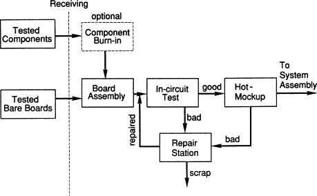
During hot-mockup test, an operator attaches the board under test to a PC-driven hard-disk assembly using clamps and pogo pins. He or she then executes intense read/modify/write cycles for 5 min or more. If the drive fails, the board is bad. One prominent disk-drive manufacturer employs more than 400 such hot mockups in one Singapore factory, with four per operator on a 5-ft workbench. To change quickly from one board to another, the operator simply pulls two cables, four thumb screws, and four Allen screws.
One fault that only hot-mockup testing can find relates to the way in which disk drives store files wherever there is empty space, often scattering many file pieces across the disk surface. Conventional test scans the disk from the outside in or the inside out. A hot-mockup test executes a read cycle on a fragmented file, stops in the middle, moves the heads, and reads the next segment. A data discontinuity between file segments indicates faulty board logic.
Hot mockup is attractive because, in most cases, the self-tests that it runs already exist. Engineering teams develop self-tests with new products. Therefore, this approach minimizes test's impact on frantic development schedules. The engine, in this case a conventional PC, already exists, as does the target system, so hardware and software development costs are very low.
On the minus side, hot mockup is very labor intensive. Results are qualitative, not quantitative, and fault diagnosis depends more on operator experience than on the test itself. Little information is available on fault coverage. Perhaps most inconvenient is the problem of mockup-system wearout. Again referring to the disk-drive manufacturer, consider the logistics of managing 400 sets of test apparatus. Replacing them only when they die is probably the least expensive option, but possibly the most disruptive to the manufacturing cycle. Replacing them all on a schedule, either a few at a time or all at once, minimizes unanticipated failures but increases hardware costs.
Because commercially available functional testers cope better with the challenges of certain products, some manufacturers are again selecting to abandon or considering abandoning hot mockup in favor of that option.
18.3.14. Architectural Models
Dividing testers into MDAs, in-circuit testers, and so on categorizes them by test method. Within each group, it is possible to separate members by tester architecture into monolithic, rack-and-stack, and hybrid systems.
Monolithic testers are the machines traditionally associated with automatic test equipment (ATE). These are single—often large—boxes from one vendor, containing a computer engine and a collection of stimulus and measurement electronics. Measurement architecture is generally unique to that vendor, although most vendors today use a standard computer engine, such as a PC-type or UNIX workstation, to avoid developing and maintaining computer-bound system software. The vendor defines the machine's overall capability. Customers must meet additional requirements through individual instruments over a standard bus, such as IEEE-488.
One advantage of the monolithic approach is that individual measurement capabilities lack unnecessary features, such as front panels, embedded computer functions, displays, and redundant software, that can make instrument-bound solutions more awkward and more expensive. The vendor generally provides a well-integrated software package and supports it directly, an advantage of “one-stop shopping” for test-program development. The vendor is familiar with every part of the system and how the parts interact, permitting the most effective service and support.
On the other hand, these systems are quite inflexible. If a customer wants a capability that the tester does not already have, one option is IEEE-488 instruments. Expandability is limited to instruments and vendor offerings. A functional tester may contain 256 pins, and the architecture may permit up to 512. The customer can expand to that point, but not beyond. The vendor may offer other features as field upgrades, but only those features are available. Add-on instrument choices are somewhat limited, and they often do not integrate well into system software. Programming the instruments requires one of the “point-and-click” programming tools or—as a last resort—that marvel of cryptic horrors, IEEE-488 language.
Rack-and-stack systems consist of a computer engine, (usually a PC-type), a switching matrix, and an array of instruments, communicating over a common I/O bus such as IEEE-488. Rack-and-stack solutions permit purchasing appropriate instruments from any vendor, as long as they support the communication bus. Therefore, this solution provides the most flexible hardware choices. It may also provide the best-quality hardware. The best switching matrix may come from vendor A, the function generator and spectrum analyzer from vendor B, the waveform analyzer from vendor C, and the logic analyzer from vendor D. Because it permits foregoing capability that the customer does not need, rack-and-stack systems may be less expensive than monolithic or hybrid solutions.
Some vendors will act as consultants, helping customers to assemble rack-and-stack systems from components, regardless of individual-instrument manufacturer. This is a handy service, as long as the vendor is honest about recommending, purchasing, and pricing competitors' products.
For analog and high-frequency applications, rack-and-stack solutions are often more accurate, less expensive, and easier to use than an array of instruments attached to a monolithic tester. In addition, some capabilities are available only as individual instruments. For an application that requires them, there is no other choice.
Disadvantages to this approach include test-program generation, which remains primarily a manual process. A user teaches the “tester” about instruments in the system and loads vendor-supplied or in-house-developed instrument drivers. Automatic software tools then guide the programmer through code creation. Although these tools can analyze information from computer-aided design and other CAE equipment, people must still create and select the final tests.
Bus-based test systems tend to be noisy, limiting measurement precision and possibly compromising functional board performance. Users must generally design their own fixtures or other interfaces between tester and board under test.
Hybrid systems offer some features of monolithic and rack-and-stack alternatives. They consist of an embedded or stand-alone computer engine, again usually a PC-type, and a collection of printed-circuit-board-based instrument modules connected through a standard I/O bus designed specifically for this purpose. The current frontrunner for this arrangement is the VME eXtension for Instrumentation—VXI—along with its more recent siblings, such as MXI and PXI.
VXI provides what the IEEE-488 bus would call the switching matrix as a special card cage. The standard specifies how to connect the modules, and the signals that allow them to communicate. This architecture permits I/O speeds of about 10 MHz and as many as 255 individual instruments, all of which may be talkers. Board and system manufacturers are beginning to create in-house-built testers around this design. In addition, traditional “monolithic” tester vendors are adopting VXI to create modular systems that increase the flexibility and expandability of the monolithic option.
The hybrid-system approach incorporates the best compromise between monolithic and rack-and-stack alternatives. Ideally, hardware and software integration resembles the monoliths, as do programming and data-analysis features. Because instrument modules are available from numerous manufacturers, test engineers can select capabilities that best match their needs. As with rack-and-stack choices, users can adopt new instrument products that improve system performance with a minimum of effort.
Disadvantages include the technique's relative immaturity compared to IEEE-488. Instrument choices are, at present, still more limited. Also, this option is still slower than many monolithic products, and users must generally create system-level and other high-level software.
The VXI standard represents a compromise among costs, features, and ease of implementation. The same can be said of de facto standards for MXI and PXI. They cannot accommodate absolutely every function that every instrument vendor can conceive of. Lead lengths in the cage and other architectural limitations mean that noise and timing can be a concern in critical situations. Board manufacturers requiring low noise and very precise timing may not be able to adopt this solution. In addition, system developers still have to design test fixtures, and users must construct them.
18.3.15. Other Options
Manual testing consists of training technicians to analyze board performance using an array of individual instruments and some kind of written procedure. The approach is most appropriate in small companies and other low-volume applications. It can also provide a good way to analyze very early production runs for a new product, where information from manual tests helps programmers develop automatic tests. Startup costs are relatively low—the cost of people, training, and instruments. The method is quite flexible if technicians move easily from one board type to another. Of course, the technique is too slow for many applications. It requires highly skilled and well-trained people, and results may be inconsistent from technician to technician or from day to day.
Inspection techniques are also gaining popularity to complement or supplement traditional test.
The most interesting alternative board-test strategy is not to test at all, as with Japanese television manufacturers. Test engineering is perhaps the only occupation whose ultimate goal is its own demise. Ensuring vendor material quality and monitoring the production process at every step will, at some point, produce 100% good boards and systems. Test professionals can rest assured, however, that we will not likely achieve that goal anytime soon.
18.4. Summary
Finding a fault at any production stage can cost 10 times what it costs to find that same fault at the preceding stage. Monitoring processes to prevent problems from occurring at all represents the least expensive option. Failing that approach, manufacturers generally try to remove as many failures as possible at board level, before assembling systems.
Many test techniques are available to accomplish this task. Bed-of-nails methods, such as shorts and opens, manufacturing-defects analysis, and in-circuit testing, operate on individual components, board traces, or functional clusters to ensure correct assembly. Most test failures have one and only one cause, minimizing diagnostic efforts.
Functional-test techniques, which control boards through a few nodes at the edge connector or a test connector, examine overall board behavior and verify it against designer intentions. Because of the logic depth between a failing node and the access point, fault diagnosis can be lengthy and may involve guided probing or other additional steps.
Emulation testers perform a functional-type test on microprocessor-based logic. Hardware pods instead of software models mimic complex circuitry, allowing testers to examine logic states and assess board performance.
Ultimately, the goal is to have processes that are sufficiently in control to eliminate test completely. Fortunately, it will be some time before that goal comes within reach.