
Chapter Sampling
Hardware characteristics such as nonlinearity, response times, and susceptibility to noise can have important consequences in a data-acquisition system. They often limit performance and may necessitate countermeasures to be implemented in software. A detailed knowledge of the transfer characteristics and temporal performance of each element of the data acquisition and control (DA&C) system is a prerequisite for writing reliable interface software. The purpose of this chapter is to draw your attention to those attributes of sensors, actuators, signal conditioning, and digitization circuitry that have a direct bearing on software design. While precise details are generally to be found in manufacturer' literature, the material presented in the following sections high- lights some of the fundamental considerations involved. Readers are referred to Eggebrecht (1990) or Tompkins and Webster (1988) for additional information.
1. Introduction
DA&C involves measuring the parameters of some physical process, manipulating the measurements within a computer, and then issuing signals to control that process. Physical variables such as temperature, force, or position are measured with some form of sensor. This converts the quantity of interest into an electrical signal which can then be processed and passed to the PC. Control signals issued by the PC are usually used to drive external equipment via an actuator such as a solenoid or electric motor.
Many sensors are actually types of transducer. The two terms have different meanings, although they are used somewhat interchangeably in some texts. Transducers are devices that convert one form of energy into another. They encompass both actuators and a subset of the various types of sensor.
1.1. Signal Types
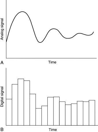
The signals transferred in and out of the PC may each be one of two basic types: analog or digital. All signals will generally vary in time. In changing from one value to another, analog signals vary smoothly (i.e., continuously), always assuming an infinite sequence of intermediate values during the transition. Digital signals, on the other hand, are discontinuous, changing only in discrete steps as shown in Figure 1.
Figure 1. Diagram contrasting (A) analog and (B) digital signals.
Digital data are generally stored and manipulated within the PC as binary integers. As most readers will know, each binary digit (bit) may assume only one of two states: low or high. Each bit can, therefore, represent only a zero or a one. Larger numbers, which are needed to represent analog quantities, are generally coded as combinations of typically 8, 12, or 16 bits. Binary numbers can only change in discrete steps equal in size to the value represented by the least significant bit (LSB). Because of this, binary (i.e., digital) representations of analog signals cannot reflect signal variations smaller than the value of the LSB. The principal advantage of digital signals is that they tend to be less susceptible than their analog counterparts to distortion and noise. Given the right communication medium, digital signals are better suited to long-distance transmission and to use in noisy environments.
Pulsed signals are an important class of digital signals. From a physical point of view, they are basically the same as single-bit digital signals. The only difference is in the way in which they are applied and interpreted. It is the static bit patterns (the presence, or otherwise, of certain bits) that are the important element in the case of digital signals. Pulsed signals, on the other hand, carry information only in their timing. The frequency, duration, duty cycle, or absolute number of pulses are generally the only significant characteristics of pulsed signals. Their amplitude does not carry any information.
Analog signals carry information in their magnitude (level) or shape (variation over time). The shape of analog signals can be interpreted either in the time or frequency domain. Most “real-world” processes that we might wish to measure or control are intrinsically analog in nature.
It is important to remember, however, that the PC can read and write only digital signals. Some sensing devices, such as switches or shaft encoders, generate digital signals that can be directly interfaced to one of the PC's I/O ports. Certain types of actuator, such as stepper motors or solenoids, can also be controlled via digital signals output directly from the PC. Nevertheless, most sensors and actuators are purely analog devices and the DA&C system must, consequently, incorporate components to convert between analog and digital representations of data. These conversions are carried out by means of devices known as analog-to-digital converters (ADCs) or digital-to-analog converters (DACs).
1.2. Elements of a DA&C System
A typical PC-based DA&C system might be designed to accept analog inputs from sensors as well as digital inputs from switches or counters. It might also be capable of generating analog and digital outputs for controlling actuators, lamps, or relays. Figure 2 illustrates the principal elements of such a system. Note that, for clarity, this figure does not include control signals. You should bear in mind that, in reality, a variety of digital control lines will be required by devices such as multiplexers, programmable-gain amplifiers, and ADCs. Depending upon the type of system in use, the device generating the control signals may be either the PC itself or dedicated electronic control circuitry.
Figure 2. A typical PC-based DA&C system.
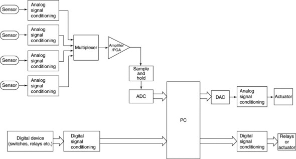
The figure shows four separate component chains representing analog input, analog output, digital input, and digital output. An ADC and DAC shown in the analog I/O chains facilitate conversion between analog and digital data formats.
Digital inputs can be generated by switches, relays, or digital electronic components such as timer/counter ICs. These signals usually have to undergo some form of digital signal conditioning, which might include voltage level conversion, isolation, or buffering, before being input via one of the PC's I/O ports. Equally, low-level digital outputs generated by the PC normally have to be amplified and conditioned in order for them to drive actuators or relays.
A similar consideration applies to analog outputs. Most actuators have relatively high current requirements which cannot be satisfied directly by the DAC. Amplification and buffering (implemented by the signal conditioning block) is, therefore, usually necessary in order to drive motors and other types of actuator.
The analog input chain is the most complex. It usually incorporates not only signal-conditioning circuits, but also components such as a multiplexer, programmable-gain amplifier (PGA), and sample-and-hold (S/H) circuit. These devices are discussed later in this chapter. The example shown is a four-channel system. Signals from four sensors are conditioned and one of the signals is selected by the multiplexer under software control. The selected signal is then amplified and digitized before being passed to the PC.
The distinction between elements in the chain is not always obvious. In many real systems the various component blocks are grouped within different physical devices or enclosures. To minimize noise, it is common for the signal-conditioning and preamplification electronics to be separated from the ADC and from any other digital components. Although each analog input channel has only one signal-conditioning block in Figure 2, this block may, in reality, be physically distributed along the analog input chain. It might be located within the sensor or at the input to the ADC. In some systems, additional components are included within the chain, or some elements, such as the S/H circuit, might be omitted.
The digital links in and out of the PC can take a variety of forms. They may be direct (although suitably buffered) connections to the PC's expansion bus, or they may involve serial or parallel transmission of data over many meters. In the former case, the ADC, DAC, and associated interface circuitry are often located on I/O cards which can be inserted in one of the PC's expansion bus slots or into a PCMCIA slot. In the case of devices that interface via the PC's serial or parallel ports, the link is implemented by appropriate transmitters, bus drivers, and interface hardware (which are not shown in Figure 2).
2. Digital I/O
Digital (including pulsed) signals are used for interfacing to a variety of computer peripherals as well as for sensing and controlling DA&C devices. Some sensing devices, such as magnetic reed switches, inductive proximity switches, mechanical limit switches, relays, or digital sensors, are capable of generating digital signals that can be read into the PC. The PC may also issue digital signals for controlling solenoids, audio-visual indicators, or stepper motors. Digital I/O signals are also used for interfacing to digital electronic devices such as timer/counter ICs or for communicating with other computers and programmable logic controllers (PLCs).
Digital signals may be encoded representations of numeric data or they may simply carry control or timing information. The latter are often used to synchronize the operation of the PC with external equipment using periodic clock pulses or handshaking signals. Handshaking signals are used to inform one device that another is ready to receive or transmit data. They generally consist of level-active, rather than pulsed, digital signals and they are essential features of most parallel and serial communication systems. Pulsed signals are not only suitable for timing and synchronization, they are also often used for event counting or frequency measurement. Pulsed inputs, for pacing or measuring elapsed time, can be generated either by programmable counter/timer ICs on plug-in DA&C cards or by programming the PC's own built-in timers. Pulsed inputs are often used to generate interrupts within the PC in response to specific external events.
2.1. TTL-Level Digital Signals
Transistor/transistor logic (TTL) is a type of digital signal characterized by nominal “high” and “low” voltages of +5V and 0V. TTL devices are capable of operating at high speeds. They can switch their outputs in response to changing inputs within typically 20 ns and can deal with pulsed signals at frequencies up to several tens of megahertz. TTL devices can also be directly interfaced to the PC. The main problem with using TTL signals for communicating with external equipment is that TTL ICs have a limited current capacity and are suitable for directly driving only low-current (i.e., a few milliamps) devices such as other TTL ICs, LEDs, and transistors. Another limitation is that TTL is capable of transmission over only relatively short distances. While it is ideal for communicating with devices on plug-in DA&C cards, it cannot be used for long-distance transmission without using appropriate bus transceivers.
The PC's expansion bus, and interface devices such as the Intel 8255 programmable peripheral interface (PPI), provide TTL-level I/O ports through which it is possible to communicate with peripheral equipment. Many devices that generate or receive digital level or pulsed signals are TTL compatible and so no signal conditioning circuits, other than perhaps simple bus drivers or tristate buffers, are required. Buffering, optical isolation, electromechanical isolation, and other forms of digital signal conditioning may be needed in order to interface to remote or high-current devices such as electric motors or solenoids.
2.2. Digital Signal Conditioning and Isolation
Digital signals often span a range of voltages other than the 0 to 5V encompassed by TTL. Many pulsed signals are TTL compatible, but this is not always true of digital level signals. Logic levels higher or lower than the standard TTL voltages can easily be accommodated by using suitable voltage attenuating or amplification components. Depending upon the application, the way in which digital I/O signals are conditioned will vary. Many applications demand a degree of isolation and/or current driving capability. The signal-conditioning circuits needed to achieve this may reside either on digital I/O interface cards which are plugged into the PC's expansion bus or they may be incorporated within some form of external interface module. Interface cards and DA&C modules are available with various degrees of isolation and buffering. Many low-cost units provide only TTL-level I/O lines. A greater degree of isolation and noise immunity is provided by devices that incorporate optical isolation and/or mechanical relays.
TTL devices can operate at high speeds with minimal propagation delay. Any time delays that may be introduced by TTL devices are generally negligible when compared with the execution time of software I/O instructions. TTL devices and circuits can thus be considered to respond almost instantaneously to software IN and OUT instructions. However, this is not generally true when additional isolating or conditioning devices are used. Considerable delays can result from using relays in particular, and these must be considered by the designer of the DA&C software.
2.2.1. Opto-Isolated I/O
It is usually desirable to electrically isolate the PC from external switches or sensors in order to provide a degree of overvoltage and noise protection. Opto-isolators can provide isolation from typically 500V to a few kilovolts at frequencies up to several hundred kilohertz. These devices generally consist of an infrared LED optically coupled to a phototransistor within a standard DIL package as shown in Figure 3. The input and output parts of the circuit are electrically isolated. The digital signal is transferred from the input (LED) circuit to the output (phototransistor) by means of an infrared light beam. As the input voltage increases (i.e., when a logical high level is applied), the photodiode emits light which causes the phototransistor to conduct. Thus the output is directly influenced by the input state while remaining electrically isolated from it.
Figure 3. Typical opto-isolator DIL packages: (A) an opto-triac suitable for mains switching, and (B) a simple opto-transistor device.
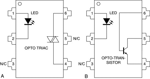
Some opto-isolating devices clean and shape the output pulse by means of built-in Schmitt triggers. Others include Darlington transistors for driving medium current loads such as lamps or relays. Mains and other AC loads maybe driven by solid-state relays which are basically opto-isolators with a high AC current switching capability.
Opto-isolators tend to be quite fast in operation, although somewhat slower than TTL devices. Typical switching times range from about 3 ms to 100 ms, allowing throughputs of about 10–300 Kbit/s. Because of their inherent isolation and slower response times, opto-isolators tend to provide a high degree of noise immunity and are ideally suited to use in noisy industrial environments. To further enhance rejection of spurious noise spikes, opto-isolators are sometimes used in conjunction with additional filtering and pulse-shaping circuits. Typical filters can increase response times to, perhaps, several milliseconds. It should be noted that opto-couplers are also available for isolating analog systems. The temporal response of any such devices used in analog I/O channels should be considered as it may have an important bearing on the sampling rate and accuracy of the measuring system.
2.2.2. Mechanical Relays and Switches
Relays are electromechanical devices that permit electrical contacts to be opened or closed by small driving currents. The contacts are generally rated for much larger currents than that required to initiate switching. Relays are ideal for isolating high-current devices, such as electric motors, from the PC and from sensitive electronic control circuits. They are commonly used on both input and output lines. A number of manufacturers provide plug-in PC interface cards with typically 8 or 16 PCB-mounted relays. Other digital output cards are designed to connect to external arrays or racks of relays.
Most relays on DA&C interface cards are allocated in arrays of 8 or 16, each one corresponding to a single bit in one of the PC's I/O ports. In many (but not all) cases, a high bit will energize the relay. Relays provide either normally open (NO) or normally closed (NC) contacts or both. NO contacts remain open until the relay coil is energized, at which point they close. NC contacts operate in the opposite sense. Ensure that you are aware of the relationship between the I/O bit states and the state of the relay contacts you are using. It is prudent to operate relays in fail-safe mode, such that their contacts return to an inactive (and safe) state when deenergized. Exactly what state is considered inactive will depend upon the application.
Because of the mass of the contacts and other mechanical components, relay switching operations are relatively slow. Small relays with low current ratings tend to operate faster than larger devices. Reed relays rated at around 1A, 24V (DC) usually switch within about 0.25 to 1 ms. The operating and release times of miniature relays rated at 1 to 3A usually fall in the range from about 2 to 5 ms. Larger relays for driving high-power DC or AC mains loads might take up to 10 or 20 ms to switch. These figures are intended only as rough guidelines. You should consult your hardware manufacturer's literature for precise switching specifications.
Switch and Relay Debouncing
When mechanical relay or switch contacts close, they tend to vibrate or bounce for a short period. This results in a sequence of rapid closures and openings before the contacts settle into a stable state. The time taken for the contacts to settle (known as the bounce time) may range from a few hundred microseconds for small reed relays up to several milliseconds for high-power relays. Because bouncing relay contacts make and break several times, it can appear to the software monitoring the relay that several separate switching events occur each time the relay is energized or deenergized. This can be problematic, particularly if the system is designed to generate interrupts as a result of each contact closure.
There are two ways in which this problem can be overcome: hardware debouncing and software debouncing. The hardware method involves averaging the state of the switch circuit over an interval of a few milliseconds so that any short-lived transitions are smoothed out and only a gradual change is recorded. A typical method is to use a resistor/capacitor (RC) network in conjunction with an inverting Schmitt buffer. Tooley (1995) discusses hardware debouncing in more detail and illustrates several simple debouncing circuits.
The software debouncing technique is suitable only for digital inputs driven from relays and switches. It cannot of course be applied to relay signals generated by the PC. The technique works by repeatedly reading the state of the relay contact. The input should be sensed at least twice and a time delay sufficient to allow the contacts to settle should be inserted between the two read operations. If the state of the contacts is the same during both reads, that state is recorded. If it has changed, further delays and read operations should be performed until two successive read operations return the same result. An appropriate limit must, of course, be imposed on the number of repeats that are allowed during the debounce routine in order to avoid the possibility of unbounded software loops. Listing 1 illustrates the debouncing technique. It assumes that the state of the relay contacts is indicated by bit 0 of I/O port 300h. The routine exits with a nonzero value in CX and the debounced relay state in bit 0 of AL. If the relay does not reach a steady state after four read operations (i.e., three delay periods), CX contains zero to indicate the error condition. The routine can easily be adapted to deal with a different bit or I/O port address.
Listing 1. Contact debouncing algorithm
- mov dx,300h ;Port number 300h for sensing relay
- mov cx,4 ;Initialize timeout counter
- DBRead: in al,dx ;Read relay I/O port
- and al,01h ;Isolate relay status bit (bit 0)
- cmp cx,4 ;Is this the first read ?
- je DBLoop ; - Yes, do another
- cmp al,bl ; - No, was relay the same as last time ?
- je DBExit ; - Yes, relay in steady state so exit
- DBLoop: mov bl,al ;Store current relay state
- call DBDelay ;Do delay to allow relay contacts to settle
- loop DBRead ;Read again, unless timed out
- DBExit:
The delay time between successive read operations (implemented by the DBDelay subroutine which is not shown) should be chosen to be just long enough to encompass the maximum contact bounce period expected. For most mechanical switches, this will be typically several milliseconds (or even tens of milliseconds for some larger devices). As a rough rule of thumb, the smaller the switch (i.e., the lower the mass of the moving contact), the shorter will be the contact bounce period. In choosing the delay time, remember to take account of the time constant of any other circuitry that forms part of the digital input channel.
Listing 1 is not totally foolproof: It will fail if the contact bounce period exactly coincides with the time period between samples. To improve the efficiency of this technique, you may wish to adapt Listing 1 in order to check that the final relay state actually remains stable for a number of consecutive samples over an appropriate time interval.
3. Sensors for Analog Signals
Sensors are the primary input element involved in reading physical quantities (such as temperature, force, or position) into a DA&C system. They are generally used to measure analog signals although the term sensor does in fact encompass some digital devices such as proximity switches. In this section we will deal only with sensing analog signals.
Analog signals can be measured with sensors that generate either analog or digital representations of the quantity to be measured (the measurand). The latter are often the simplest to interface to the PC as their output can be read directly into one the PC's I/O ports via a suitable digital input card. Examples of sensors with digital outputs include shaft encoders and some types of flow sensor.
Most types of sensor operate in a purely analog manner, converting the measurand to an equivalent analog signal. The sensor output generally takes the form of a change in some electrical parameter such as voltage, current, capacitance, or resistance. The primary purpose of the analog signal-conditioning blocks shown in Figure 2 is to precondition the sensors' electrical outputs and to convert them into voltage form for processing by the ADC.
You should be aware of a number of important sensor characteristics in order to successfully design and write interface software. Of most relevance are accuracy, dynamic range, stability, linearity, susceptibility to noise, and response times. The last includes rise time and settling time and is closely related to the sensor's frequency response.
Sensor characteristics cannot be considered in isolation. Sensors are often closely coupled to their signal-conditioning circuits and we must, therefore, also take into account the performance of this component when designing a DA&C system. Signal-conditioning and digitization circuitry can play an important (if not the most important) role in determining the characteristics of the measuring system as a whole. Although signal-conditioning circuits can introduce undesirable properties of their own, such as noise or drift, they are usually designed to compensate for inadequacies in the sensor's response. If properly matched, signal-conditioning circuits are often able to cancel out sensor offsets, nonlinearities, or temperature dependencies. We will discuss signal conditioning later in this chapter.
3.1. Accuracy
Accuracy represents the precision with which a sensor can respond to the measurand. It refers to the overall precision of the device resulting from the combined effect of offsets and proportional measurement errors. When assessing accuracy, one must take account of manufacturers' figures for repeatability, hysteresis, stability, and if appropriate, resolution. Although a sensor's accuracy figure may include the effect of resolution, the two terms must not be confused. Resolution represents the smallest change in the measurand that the sensor can detect. Accuracy includes this but also encompasses other sources of error.
3.2. Dynamic Range
A sensor's dynamic range is the ratio of its full-scale value to the minimum detectable signal variation. Some sensors have very wide dynamic ranges, and if the full range is to be accommodated, it may be necessary to employ high-resolution ADCs or Programmable- gain amplifiers. Using a PGA might increase the system's data-storage requirements, because of the addition of an extra variable (i.e., gain). These topics are discussed further in the section “Amplification and Extending Dynamic Range” later in this chapter.
3.3. Stability and Repeatability
The output from some sensors tends to drift over time. Instabilities may be caused by changes in operating temperature or by other environmental factors. If the sensor is likely to exhibit any appreciable instability, you should assess how this can be compensated for in the software. You might wish, for example, to include routines that force the operator to recalibrate or simply rezero the sensor at periodic intervals. Stability might also be compromised by small drifts in the supplied excitation signals. If this is a possibility, the software should be designed to monitor the excitation voltage using a spare analog input channel and to correct the measured sensor readings accordingly.
3.4. Linearity
Most sensors provide a linear output—that is, their output is directly proportional to the value of the measurand. In such cases the sensor response curve consists of a straight line. Some devices such as thermocouples do not exhibit this desirable characteristic. If the sensor output is not linearized within the signal-conditioning circuitry, it will be necessary for the software to correct for any nonlinearities present.
3.5. Response Times
The time taken by the sensor to respond to an applied stimulus is obviously an important limiting factor in determining the overall throughput of the system. The sensor's response time (sometimes expressed in terms of its frequency response) should be carefully considered, particularly in systems that monitor for dangerous, overrange, or otherwise erroneous conditions. Many sensors provide a virtually instantaneous response and in these cases it is usually the signal-conditioning or digitization components (or, indeed, the software itself) that determines the maximum possible throughput. This is not generally the case with temperature sensors, however. Semiconductor sensors, thermistors, and thermocouples tend to exhibit long response times (upwards of 1 s). In these cases, there is little to be gained (other than the ability to average out noise) by sampling at intervals shorter than the sensor's time constant.
You should be careful when interpreting response times published in manufacturers' literature. They often relate to the time required for the sensor's output to change by a fixed fraction in response to an applied step change in temperature. If a time constant is specified it generally defines the time required for the output to change by 1 – e−1 (i.e., about 63.21%) of the difference between its initial and final steady state outputs. The response time will be longer if quoted for a greater fractional change. The response time of thermal sensors will also be highly dependent upon their environment. Thermal time constants are usually quoted for still air, but much faster responses will apply if the sensor is immersed in a free-flowing or stirred liquid such as oil or water.
3.6. Susceptibility to Noise
Noise is particularly problematic with sensors that generate only low-level signals (e.g., thermocouples and strain gauges). Low-pass filters can be used to remove noise which often occurs predominantly at higher frequencies than the signals to be measured. Steps should always be taken to exclude noise at its source by adopting good shielding and grounding practices. As signal-conditioning circuits and cables can introduce noise themselves, it is essential that they are well designed. Even when using hardware and electronic filters, there may still be some residual noise on top of the measured signal. A number of filtering techniques can be employed in the software and some of these are discussed later in the chapter.
3.7. Some Common Sensors
This section describes features of several common sensors that are relevant to DA&C software design. Unfortunately, space does not permit an exhaustive list. Many sensors that do not require special considerations or software techniques are excluded from this section. Some less widely used devices, such as optical and chemical sensors are also excluded, even though they are often associated with problems such as long response times and high noise levels. Details of the operation of these devices may be found in specialist books such as Tompkins and Webster (1988), Parr (1986), or Warring and Gibilisio (1985).
The information provided here is typical for each type of sensor described. However, different manufacturers' implementations vary considerably. The reader is advised to consult manufacturers' data sheets for precise details of the sensor and signal-conditioning circuits that they intend to use.
3.8. Digital Sensors and Encoders
Some types of sensor convert the analog measurand into an equivalent digital representation that can be transferred directly to the PC. Digital sensors tend to require minimal signal conditioning.
As mentioned previously the simplest form of digital sensor is the switch. Examples include inductive proximity switches and mechanical limit switches. These produce a single-bit input that changes state when some physical parameter (e.g., spatial separation or displacement) rises above, or falls below, a predefined limit. However, to measure the magnitude of an analog quantity, we need a sensor with a response that varies in many (typically several hundred or more) steps over its measuring range. Such sensors are more correctly known as encoders as they are designed to encode the measurand into a digital form.
Sensors such as the rotor tachometer employ magnetic pickups which produce a stream of digital pulses in response to the rotation of a ferrous disk. Angular velocity or incremental changes in angular position can be measured with these devices. The pulse rate is proportional to the angular velocity of the disk. Similar sensors are available for measuring linear motion.
Shaft encoders are used for rotary position or velocity measurement in a wide range of industrial applications. They consist of a binary encoded disk that is mounted on a rotating shaft or spindle and located between some form of optical transmitter and matched receiver (e.g., infrared LEDs and phototransistors). The bit pattern detected by the receiver will depend upon the angular position of the encoded disk. The resolution of the system might be typically ±1°.
A disk encoded in true (natural) binary has the potential to produce large errors. If, for example, the disk is very slightly misaligned, the most significant bit might change first during a transition between two adjacent encoded positions. Such a situation can give rise to a momentary 180° error in the output. This problem is circumvented by using the Gray code. This a binary coding scheme in which only one bit changes between adjacent coded positions. The outputs from these encoders are normally converted to digital pulse trains which carry rotary position, speed, and direction information. Because of this it is rarely necessary for the DA&C programmer to use binary Gray codes directly. We will, however, discuss other binary codes later in this chapter.
The signals generated by digital sensors are often not TTL compatible, and in these cases additional circuitry is required to interface to the PC. Some or all of this circuitry may be supplied with (or as part of) the sensor, although certain TTL buffering or opto-isolation circuits may have to be provided on separate plug-in digital interface cards.
Digital position encoders are inherently linear, stable, and immune to electrical noise. However, care has to be taken when absolute position measurements are required, particularly when using devices that produce identical pulses in response to incremental changes in position. The measurement must always be accurately referenced to a known zero position. Systematic measurement errors can result if pulses are somehow missed or not counted by the software. Regular zeroing of such systems is advisable if they are to be used for repeated position measurements.
3.8.1. Potentiometric Sensors
These very simple devices are usually used for measurement of linear or angular position. They consist of a resistive wire and sliding contact. The resistance to the current flowing through the wire and contact is a measure of the position of the contact. The linearity of the device is determined by the resistance of the output load, but with appropriate signal conditioning and buffering, nonlinearities can generally be minimized and may, in fact, be negligible. Most potentiometric sensors are based on closely wound wire coils. The contact slides along the length of the coil, and as it moves across adjacent windings, it produces a stepped change in output. These steps may limit the resolution of the device to typically 25 to 50 mm.
3.8.2. Semiconductor Temperature Sensors
This class of temperature sensor includes devices based on discrete diodes and transistors as well as temperature-sensitive integrated circuits. Most of these devices are designed to exhibit a high degree of stability and linearity. Their working range is, however, relatively limited. Most operate from about −50 to +150° C, although some devices are suitable for use at temperatures down to about −230° C or lower. IC temperature sensors are typically linear to within a few degrees centigrade. A number of ICs and discrete transistor temperature sensors are somewhat more linear than this: perhaps ±0.5 to ±2° C or better. The repeatability of some devices may be as low as ±0.01° C.
All thermal sensors tend to have quite long response times. Their time constants are dependent upon the rate at which temperature changes are conducted from the surrounding medium. The intrinsic time constants of semiconductor sensors are usually of the order of 1–10s. These figures assume efficient transmission of thermal energy to the sensor. If this is not the case, much longer time constants will apply (e.g., a few seconds to about a minute in still air).
Most semiconductor temperature sensors provide a high-level current or voltage output that is relatively immune to noise and can be interfaced to the PC with minimal signal conditioning. Because of the long response times, software filtering can be easily applied should noise become problematic.
3.8.3. Thermocouples
Thermocouples are very simple temperature measuring devices. They consist of junctions of two dissimilar metal wires. An electromotive force (emf) is generated at each of the thermocouple's junctions by the Seeback effect. The magnitude of the emf is directly related to the temperature of the junction. Various types of thermocouple are available for measuring temperatures from about −200° C to in excess of 1800° C. There are a number of considerations that must be borne in mind when writing interface software for thermocouple systems.
Depending upon the type of material from which the thermocouple is constructed, its output ranges from about 10 to 70 μmV/° C. Thermocouple response characteristics are defined by various British and international standards. The sensitivity of thermocouples tends to change with temperature and this gives rise to a nonlinear response. The nonlinearity may not be problematic if measurements are to be confined to a narrow enough temperature range, but in most cases there is a need for some form of linearization. This may be handled by the signal conditioning circuits, but it is often more convenient to linearize the thermocouple' output by means of suitable software algorithms.
Even when adequately linearized, thermocouple-based temperature measuring systems are not awfully accurate, although it has to be said that they are often more than adequate for many temperature- sensing applications. Thermocouple accuracy is generally limited by variations in manufacturing processes or materials to about 1 to 4° C.
Like other forms of temperature sensor, thermocouples have long response times. This depends upon the mass and shape of the thermocouple and its sheath. According to the Labfacility Ltd. temperature sensing handbook (1987), time constants for thermocouples in still air range from 0.05 to around 40s.
Thermocouples are rather insensitive devices. They output only low-level signals—typically less than 50 mV—and are, therefore, prone to electrical noise. Unless the devices are properly shielded, mains pickup and other forms of noise can easily swamp small signals. However, because thermocouples respond slowly, their outputs are very amenable to filtering. Heavy software filtering can usually be applied without losing any important temperature information.
3.8.4. Cold-Junction Compensation
In order to form a complete circuit, the conductors that make up the thermocouple must have at least two junctions. One (the sensing junction) is placed at an unknown temperature (i.e., the temperature to be measured) and the remaining junction (known as the cold junction or reference junction) is either held at a fixed reference temperature or allowed to vary (over a narrow range) with ambient temperature. The reference junction generates its own temperature-dependent emf which must be taken into account when interpreting the total measured thermocouple voltage.
Thermocouple outputs are usually tabulated in a form that assumes that the reference junction is held at a constant temperature of 0° C. If the temperature of the cold junction varies from this fixed reference value, the additional thermal emf will offset the sensor's response. It is not possible to calibrate out this offset unless the temperature of the cold junction is known and is constant. Instead, the cold junction's temperature is normally monitored in order that a dynamic correction may be applied to the measured thermocouple voltage.
The cold-junction temperature can be sensed using an independent device such as a semiconductor (transistor or IC) temperature sensor. In some signal-conditioning circuits, the output from the semiconductor sensor is used to generate a voltage equal in magnitude, but of opposite sign, to the thermal emf produced by the cold junction. This voltage is then electrically added to the thermocouple signal so as to cancel any offset introduced by the temperature of the cold junction.
It is also possible to perform a similar offset-canceling operation within the data-acquisition software. If the output from the semiconductor temperature sensor is read via an ADC, the program can gauge the cold-junction temperature. As the thermocouple's response curve is known, the software is able to calculate the thermal emf produced by the cold junction—that is, the offset value. This is then applied to the total measured voltage in order to determine that part of the thermocouple output due only to the sensing junction. This is accomplished as follows.
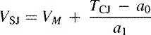
The response of the cold junction and the sensing junction both generally follow the same nonlinear form. As the temperature of the cold junction is usually limited to a relatively narrow range, it is often practicable to approximate the response of the cold junction by a straight line: (1)
![]() where TCJ is the temperature of the cold junction in degrees Centigrade, VCJ is the corresponding thermal emf and a0 and a1 are constants that depend upon the thermocouple type and the temperature range over which the straight-line approximation
is made. Table 1 lists the parameters of straight-line approximations to the response curves of a range of different thermocouples over the temperature range from 0 to 40° C.
where TCJ is the temperature of the cold junction in degrees Centigrade, VCJ is the corresponding thermal emf and a0 and a1 are constants that depend upon the thermocouple type and the temperature range over which the straight-line approximation
is made. Table 1 lists the parameters of straight-line approximations to the response curves of a range of different thermocouples over the temperature range from 0 to 40° C.
Table 1. Parameters of straight-line fits to thermocouple response curves over the range 0 to 40° C, for use in software cold-junction compensation
| Type | a0(° C) | a1(° C mV−1) | Accuracy (° C) |
|---|---|---|---|
| K | 0.130 | 24.82 | ±0.25 |
| J | 0.116 | 19.43 | ±0.25 |
| R | 0.524 | 172.0 | ±1.00 |
| S | 0.487 | 170.2 | ±1.00 |
| T | 0.231 | 24.83 | ±0.50 |
| E | 0.174 | 16.53 | ±0.30 |
| N | 0.129 | 37.59 | ±0.40 |
The measured thermocouple voltage VM is equal to the difference between the thermal emf produced by the sensing junction (VSJ) and the cold junction (VCJ): (2)
![]()
As we are interested only in the difference in junction voltages, VSJ and VCJ can be considered to represent either the absolute thermal emfs produced by each junction or the emfs relative to whatever junction voltage might be generated at some convenient temperature origin. In the following discussion we will choose the origin of the temperature scale to be 0° C (so that 0° C is considered to produce a zero junction voltage). In fact, the straight-line parameters listed in Table 1 represent an approximation to a 0° C-based response curve (a0 is close to zero).
Rearranging Equation (1) and substituting for VCJ in Equation (2), we see that (3)
The values of a0 and a1 for the appropriate type of thermocouple can be substituted from Table 1 into this equation in order to compensate for the temperature of the cold junction. All voltage values should be in millivolts and TCJ should be expressed in degrees Centigrade. The temperature of the sensing junction can then be calculated by applying a suitable linearizing polynomial to the VSJ value. Note that the polynomial must also be constructed for a coordinate system with an origin at V = 0 mV, T = 0° C.
It is interesting to note that the type B thermocouple is not amenable to this method of cold-junction compensation as it exhibits an unusual behavior at low temperatures. As the temperature rises from zero to about 21° C, the thermoelectric voltage falls to approximately −3 μV. It then begins to rise, through 0V at about 41° C, and reaches +3 μV at 52° C. It is, therefore, not possible to accurately fit a straight line to the thermocouple's response curve over this range. Fortunately, if the cold-junction temperature remains within 0 to 52° C it contributes only a small proportion of the total measured voltage (less than about ±3 μV). If the sensing junction is used over its normal working range of 600 to 1700° C, the measurement error introduced by completely ignoring the cold-junction emf will be less than ±0.6° C.
The accuracy figures quoted in Table 1 are generally better than typical thermocouple tolerances and so the a0 and a1 parameters should be usable in most situations. More precise compensation factors can be obtained by fitting the straight line over a narrower temperature range or by using a lookup table with the appropriate interpolation routines. You should calculate your own compensation factors if a different cold-junction temperature range is to be used.
3.9. Resistive Temperature Sensors (Thermistors and RTDs)
Thermistors are semiconductor or metal oxide devices whose resistance changes with temperature. Most exhibit negative temperature coefficients (i.e., their resistance decreases with increasing temperature) although some have positive temperature coefficients. Thermistor temperature coefficients range from about 1 to 5%/° C. They tend to be usable in the range −70 to +150° C, but some devices can measure temperatures up to 300° C. Thermistor-based measuring systems can generally resolve temperature changes as small as ±0.01° C, although typical devices can provide absolute accuracies no better than ±0.1 to 0.5° C. The better accuracy figure is often only achievable in devices designed for use over a limited range (e.g., 0 to 100° C).
As shown in Figure 4, thermistors tend to exhibit a highly nonlinear response. This can be corrected by means of suitable signal-conditioning circuits or by combining thermistors with positive and negative temperature coefficients. Although this technique can provide a high degree of linearity, it may be preferable to carry out linearization within the DA&C software. A third-order logarithmic polynomial is usually appropriate. The response time of thermistors depends upon their size and construction. They tend to be comparable with semiconductor temperature sensors in this respect, but because of the range of possible constructions, thermistor time constants may be as low as several tens of milliseconds or as high as 100–200s.
Figure 4. Typical resistance vs. temperature characteristics for (A) negative temperature coefficient thermistors and (B) platinum RTDs.
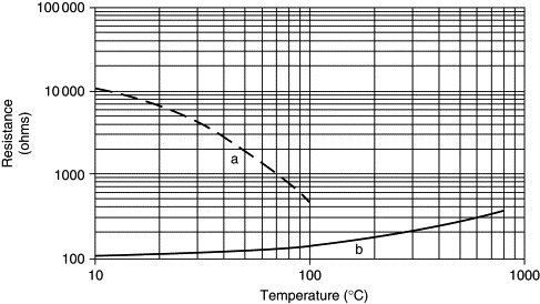
Resistance temperature detectors (RTDs) also exhibit a temperature-dependent resistance. These devices can be constructed from a variety of metals, but platinum is the most widely used. They are suitable for use over ranges of about −270 to 660° C, although some devices have been employed for temperatures up to about 1000° C. RTDs are accurate to within typically 0.2 to 4° C, depending on temperature and construction. They also exhibit a good long-term stability, so frequent recalibration may not be necessary. Their temperature coefficients are generally on the order of 0.4 Ω/° C. However, their sensitivity falls with increasing temperature, leading to a slightly nonlinear response. This nonlinearity is often small enough, over limited temperature ranges (e.g., 0 to 100° C), to allow a linear approximation to be used. Wider temperature ranges require some form of linearization to be applied: A third-order polynomial correction usually provides the optimum accuracy. Response times are comparable with those of thermistors.
3.10. Resistance Sensors and Bridges
A number of other types of resistance sensor are available. Most notable amongst these are strain gauges. These take a variety of forms, including semiconductors, metal wires, and metal foils. They are strained when subjected to a small displacement, and as the gauge becomes deformed, its resistance changes slightly. It is this resistance that is indirectly measured in order to infer values of strain, force, or pressure. The light dependent resistor (LDR) is another example of a resistance sensor. The resistance of this device changes in relation to the intensity of light impinging upon its surface.
Both thermistors and RTDs can be used in simple resistive networks, but because devices such as RTDs and strain gauges have low sensitivities, it can be difficult to directly measure changes in resistance. Bridge circuits such as that shown in Figure 5 are, therefore, often used to obtain optimum precision. The circuit is designed (or adjusted) so that the voltage output from the bridge is zero at some convenient value of the measurand (e.g., zero strain in the case of a strain gauge bridge). Any changes in resistance induced by changes in the measurand cause the bridge to become unbalanced and to produce a small output voltage. This can be amplified and measured independently of the much larger bridge-excitation voltage. Although bridge circuits are used primarily with insensitive devices, they can also be used with more responsive resistance sensors such as thermistors.
Figure 5. Bridge circuit for measuring resistance changes in strain gauges and RTDs.
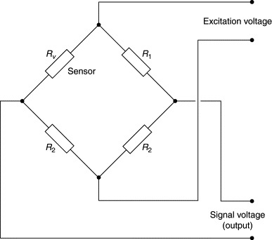
Bridges often contain two or four sensing elements (replacing the fixed resistors shown in Figure 5). These are arranged in such a way as to enhance the overall sensitivity of the bridge and, in the case of nonthermal sensors, to compensate for temperature dependencies of the individual sensing elements. This approach is used in the design of strain-gauge-based sensors such as load cells or pressure transducers.
Bridges with one sensing element exhibit a nonlinear response. Two-active-arm bridges, which have sensors placed in opposite arms, are also nonlinear. However, provided that only small fractional changes occur in the resistance of the sensing element(s), the nonlinearities of one- and two-arm bridges are often small enough that they can be ignored. Strain-gauge bridges with four active sensors generate a linear response provided that the sensors are arranged so that the resistance change occurring in one diagonally opposing pair of gauges is equal and opposite to that occurring in the other (Pople, 1979). When using resistance sensors in a bridge configuration, it is advisable to check for and, if necessary, correct any nonlinearities that may be present.
Conduction of the excitation current can cause self-heating within each sensing element. This can be problematic with thermal sensors—thermistors in particular. Temperature rises within strain gauges can also cause errors in the bridge output. Because of this, excitation currents and voltages have to be kept within reasonable limits. This often results in low signal levels. For example, in most implementations, strain-gauge bridges generate outputs of the order of a few millivolts. Because of this, strain-gauge and RTD-based measuring systems are susceptible to noise, and a degree of software or hardware filtering is frequently required.
Lead resistance must also be considered when using resistance sensors. This is particularly so in the case of low-resistance devices such as strain gauges and RTDs, which have resistances of typically 120 to 350Ω and 100 to 200Ω, respectively. In these situations even the small resistance of the lead wires can introduce significant measurement errors. The effect of lead resistance can be minimized by means of compensating cables and suitable signal conditioning. This is usually the most efficient approach. Alternatively, the same type of compensation can be performed in software by using a spare ADC channel to directly measure the excitation voltage at the location of the sensor or bridge.
3.10.1. Linear Variable Differential Transformers
Linear variable differential transformers (LVDTs) are used for measuring linear displacement. They consist of one primary and two secondary coils. The primary coil is excited with a high-frequency (typically several hundred to several thousand hertz) voltage. The magnetic-flux linkage between the concentric primary and secondary coils depends upon the position of a ferrite core within the coil geometry. Induced signals in the secondary coils are combined in a differential manner such that movement of the core along the axis of the coils results in a variation in the amplitude and phase of the combined secondary-coil output. The output changes phase at the central (null) position and the amplitude of the output increases with displacement from the null point. The high-frequency output is then demodulated and filtered in order to produce a DC voltage in proportion to the displacement of the ferrite core from its null position. The filter used is of the low-pass type which blocks the high-frequency ripple but passes lower-frequency variations due to core movement.
Obviously the excitation frequency must be high in order to allow the filter's cutoff frequency to be designed such that it does not adversely affect the response time of the sensing system. The excitation frequency should be considerably greater than the maximum frequency of core movement. This is usually the case with LVDTs. However, the filtration required with low-frequency excitation (less than a few hundred hertz) may significantly affect the system's response time and must be taken into account by the software designer.
The LVDT offers a high sensitivity (typically 100–200 mV/V at its full-scale position) and high-level voltage output that is relatively immune to noise. Software filtering can, however, enhance noise rejection in some situations.
The LVDT's intrinsic null position is very stable and forms an ideal reference point against which to position and calibrate the sensor. The resolution of an LVDT is theoretically infinite. In practice, however, it is limited by noise and the ability of the signal-conditioning circuit to sense changes in the LVDT's output. Resolutions of less than 1 mm are possible. The device's repeatability is also theoretically infinite, but is limited in practice by thermal expansion and mechanical stability of the sensor's body and mountings. Typical repeatability figures lie between ±0.1 and ±10 mm, depending upon the working range of the device. Temperature coefficients are also an important consideration. These are usually on the order of 0.01%/° C. It is wise to periodically recalibrate the sensor, particularly if it is subject to appreciable temperature variations.
LVDTs offer quite linear responses over their working range. Designs employing simple parallel coil geometries are capable of maintaining linearity over only a short distance from their null position. Nonlinearities of up to 10% or more become apparent if the device is used outside this range. In order to extend their operating range, LVDTs are usually designed with more complex and expensive graduated or stepped windings. These provide linearities of typically 0.25%. An improved linearity can sometimes be achieved by applying software linearization techniques.
4. Handling Analog Signals
Signal levels and current-loading requirements of sensors and actuators usually preclude their direct connection to ADCs and DACs. For this reason, data acquisition and control systems generally require analog signals to be processed before being input to the PC or after transmission from it. This usually involves conditioning (i.e., amplifying, filtering, and buffering) the signal. In the case of analog inputs, it may also entail selecting and capturing the signal-using devices such as multiplexers and sample-and-hold circuits.
4.1. Signal Conditioning
Signal conditioning is normally required on both inputs and outputs. In this section we will concentrate on analog inputs, but analogous considerations will apply to analogue outputs; for example, the circuits used to drive actuators.
4.1.1. Conditioning Analog Inputs
Signal conditioning serves a number of purposes. It is needed to clean and shape signals, to supply excitation voltages, to amplify and buffer low level signals, to linearize sensor outputs, to compensate for temperature-induced drifts, and to protect the PC from electrical noise and surges. The signal-conditioning blocks shown in Figure 2 may consist of a number of separate circuits and components. These elements are illustrated in Figure 6.
Figure 6. Elements of a typical analog input signal-conditioning circuit.
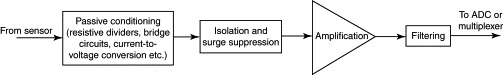
Certain passive signal-conditioning elements such as potential dividers, bridge circuits, and current-to-voltage conversion resistors are often closely coupled to the sensor itself and, indeed, may be an integral part of it. The sensor is sometimes isolated from the remaining signal-conditioning circuits and from the PC by means of linear opto-couplers or capacitively coupled devices. Surge-suppression components such as zener diodes and metal oxide varistors may also be used in conjunction with RC networks to protect against transient voltage spikes.
Because typical ADCs have sensitivities of a few millivolts per bit, it is essential to amplify the low-level signals from thermocouples, strain gauges, and RTDs (which may be only a few tens of millivolts at full scale). Depending upon the type of sensor in use, activities such as AC demodulation or thermocouple cold-junction compensation might also be performed prior to amplification. Finally, a filtering stage might be employed to remove random noise or AC excitation ripple. Low-pass filters also serve an antialiasing function as described in later in the chapter.
So what relevance does all this have to the DA&C programmer? In well-designed systems, very little—the characteristics of the signal conditioning should have no significant limiting affect on the design or performance of the software, and most of the characteristics of the sensor and signal conditioning should be transparent to the programmer. Unfortunately this is not always the case.
The amplifier and other circuits can give rise to temperature-dependent offsets or gain drifts (typically on the order of 0.002–0.010% of full scale per degree Centigrade) which may necessitate periodic recalibration or linearization. When designing DA&C software you should consider the following:
- The frequency of calibration
- The need to enforce calibration or to prompt the operator when calibration is due
- How calibration data will be input, stored, and archived
- The necessity to rezero sensors after each data-acquisition cycle
You should also consider the frequency response (or bandwidth) of the signal-conditioning circuitry. This can affect the sampling rate and limit throughput in some applications (see later). Typical bandwidths are on the order of a few hundred hertz, but this does, of course, vary considerably between different types of signal-conditioning circuit and depends upon the degree of filtration used. High-gain signal-conditioning circuits, which amplify noisy low-level signals, often require heavy filtering. This may limit the bandwidth to typically 100 to 200 Hz. Systems employing low frequency LVDTs can have even lower bandwidths. Bandwidth may not be an important consideration when monitoring slowly varying signals (e.g., temperature), but it can prove to be problematic in high-speed applications involving, for example, dynamic force or strain measurement.
If high-gain amplifiers are used and/or if hardware filtration is inadequate, it may be necessary to incorporate filtering algorithms within the software. If this is the case, you should carefully assess which signal frequencies you wish to remove and which frequencies you will need to retain, and then reconcile this with the proposed sampling rate and the software's ability to reconstruct an accurate representation of the underlying noise-free signal. Sampling considerations and software filtering techniques are discussed later in the chapter.
It may also, in some situations, be necessary for the software to monitor voltages at various points within the signal-conditioning circuit. We have already mentioned monitoring of bridge excitation levels to compensate for voltage drops due to lead-wire resistance. The same technique (sometimes known as ratiometric correction) can also be used to counteract small drifts in excitation supply. If lead-wire resistance can be ignored, the excitation voltage may be monitored either at its source or at the location of the sensor.
There is another (although rarer) instance when it might be necessary to monitor signal-conditioning voltage levels. This is when pseudo-differential connections are employed on the input to an amplifier. Analog signal connections may be made in two ways: single ended or differential. Single-ended signals share a common ground or return line. Both the signal source voltage and the input to the amplifier(s) exist relative to the common ground. For this method to work successfully, the ground potential difference between the source and amplifier must be negligible, otherwise the signal to be measured appears superimposed on a nonzero (and possibly noisy) ground voltage. If a significant potential difference exists between the ground connections, currents can flow along the ground wire causing errors in the measured signals.
Differential systems circumvent this problem by employing two wires for each signal. In this case, the signal is represented by the potential difference between the wires. Any ground-loop-induced voltage appears equally (as a common-mode signal) on each wire and can be easily rejected by a differential amplifier.
An alternative to using a full differential system is to employ pseudo-differential connections. This scheme is suitable for applications in which the common-mode voltage is moderately small. It makes use of single-ended channels with a common ground connection. This allows cheaper operational amplifiers to be used. The potential of the common ground return point is measured using a spare ADC input in order to allow the software to correct for any differences between the local and remote ground voltages. Successful implementation of this technique obviously requires the programmer to have a reasonably detailed knowledge of the signal conditioning circuitry. Unless the common-mode voltage is relatively static, this technique also necessitates concurrent sampling of the signal and ground voltages. In this case simultaneous sample-and-hold circuits (discussed later in this chapter) or multiple ADCs may have to be used.
4.1.2. Conditioning Analog Outputs
Some form of signal conditioning is required on most analog outputs, particularly those that are intended to control motors and other types of actuator. Space limitations preclude a detailed discussion of this topic, but in general, the conditioning circuits include current-driving devices and power amplifiers and the like. The nature of the signal conditioning used is closely related to the type of actuator. As in the case of analog inputs, it is prudent for the programmer to gain a thorough understanding of the actuator and associated signal-conditioning circuits in order that the software can be designed to take account of any nonlinearities or instabilities that might be present.
4.2. Multiplexers
Multiplexers allow several analog input channels to be serviced by a single ADC. They are basically software-controlled analog switches that can route 1 of typically 8 or 16 analog signals through to the input of the system's ADC. A four-channel multiplexed system is illustrated in Figure 2. A multiplexer used in conjunction with a single ADC (and possibly amplifier) can take the place of several ADCs (and amplifiers) operating in parallel. This is normally considerably cheaper, and uses less power, than an array of separate ADCs and for this reason analog multiplexers are commonly used in multichannel data acquisition systems.
However, some systems do employ parallel ADCs in order to maximize throughput. The ADCs must, of course, be well matched in terms of their offset, gain and integral nonlinearity errors. In such systems, the digitized readings from each channel (i.e., ADC) are digitally multiplexed into a data register or into one of the PC's I/O ports. From the point of view of software design, there is little to be said about digital multiplexers. In this section, we will deal only with the properties of their analog counterparts.
In an analog multiplexed system, multiple channels share the same ADC and the associated sensors must be read sequentially, rather than in parallel. This leads to a reduction in the number of channels that can be read per second. The decrease in throughput obviously depends upon how efficiently the software controls the digitization and data input sequence.
A related problem is skewing of the acquired data. Unless special S/H circuitry is used, simultaneous sampling is not possible. This is an obvious disadvantage in applications that must determine the temporal relationship or relative phase of two or more inputs.
Multiplexers can be operated in a variety of ways. The desired analog channel is usually selected by presenting a 3- or 4-bit address (i.e., channel number) to its control pins. In the case of a plug-in ADC card, the address-control lines are manipulated from within the software by writing an equivalent bit pattern to one of the card's registers (which usually appear in the PC's I/O space). Some systems can be configured to automatically scan a range of channels. This is often accomplished by programming the start and end channel numbers into a “scan register.” In contrast, some intelligent DA&C units require a high-level channel-selection command to be issued. This often takes the form of an ASCII character string transmitted via a serial or parallel port.
Whenever the multiplexer is switched between channels, the input to the ADC or S/H will take a finite time to settle. The settling time tends to be longer if the multiplexer's output is amplified before being passed to the S/H or ADC. An instrumentation amplifier may take typically 1–10 ms to settle to a 12-bit (0.025%) accuracy. The exact settling time will vary, but will generally be longest with high-gain PGAs or where the amplifier is required to settle to a greater degree of accuracy.
The settling time can be problematic. If the software scans the analog channels (i.e., switches the multiplexer) too rapidly, the input to the S/H or ADC will not settle sufficiently and a degree of apparent cross-coupling may then be observed between adjacent channels. This can lead to measurement errors of several percent, depending upon the scanning rate and the characteristics of the multiplexer and amplifier used. These problems can be avoided by careful selection of components in relation to the proposed sampling rate. Bear in mind that the effects of cross-coupling may be dependent upon the sequence as well as the frequency with which the input channels are scanned. Cross-coupling may not even be apparent during some operations. A calibration facility, in which only one channel is monitored, will not exhibit any cross-coupling, while a multichannel scanning sequence may be badly affected. It is advisable to check for this problem at an early stage of software development as, if present, it can impose severe restrictions on the performance of the system.
4.2.1. Sample-and-Hold Circuits
Many systems employ a sample-and-hold circuit on the input to the ADC to freeze the signal while the ADC digitizes it. This prevents errors due to changes in the signal during the digitization process (see later in the chapter). In some implementations, the multiplexer can be switched to the next channel in a sequence as soon as the signal has been grabbed by the S/H. This allows the digitization process to proceed in parallel with the settling time of the multiplexer and amplifier, thereby enhancing throughput. S/H circuits can also be used to capture transient signals. Software-controlled systems are not capable of responding to very high-speed transient signals (i.e., those lasting less than a few microseconds) and so, in these cases, the S/H and digitization process may be initiated by means of special hardware (e.g., a pacing clock). The software is then notified (by means of an interrupt, for example) when the digitization process is complete.
S/H circuits require only a single digital control signal to switch them between their “sample” and “hold” modes. The signal may be manipulated by software via a control register mapped to one of the PC's I/O ports, or it may be driven by dedicated onboard hardware. S/H circuits present at the input to ADCs are often considered to be an integral part of the digitization circuitry. Indeed, the command to start the analog-to-digital conversion process may also automatically activate the S/H for the required length of time.
4.2.2. Simultaneous S/H
In multiplexed systems like that represented in Figure 2, analog input channels have to be read sequentially. This introduces a time lag between the samples obtained from successive channels. Assuming typical times for ADC conversion and multiplexer/amplifier settling, this time lag can vary from several tens to several hundreds of microseconds. The consequent skewing of the sample matrix can be problematic if you wish to measure the phase relationship between dynamically varying signals. Simultaneous S/H circuits are often used to overcome this problem. Figure 7 illustrates a four-channel analog input system employing simultaneous S/H.
Figure 7. Analog input channels with simultaneous sample and hold.
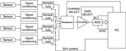
The system is still multiplexed, so very little improvement is gained in the overall throughput (total number of channels read per second), but the S/H circuits allow data to be captured from all inputs within a very narrow time interval (see the following section). Simultaneous S/H circuits may be an integral part of the signal conditioning unit or they may be incorporated in the digitization circuitry (e.g., on a plug-in ADC card). In either case they tend to be manipulated by a single digital signal generated by the PC.
4.2.3. Characteristics of S/H Circuits
When not in use, the S/H circuit can be maintained in either the sample or hold mode. To operate the device, it must first be switched into sample mode for a short period and then into hold mode in order to freeze the signal before analog-to-digital conversion begins. When switched to sample mode, the output of the S/H takes a short, but sometimes significant, time to react to its input. This time delay arises because the device has to charge up an internal capacitor to the level of the input signal. The rate of charging follows an exponential form and so a greater degree of accuracy is achieved if the capacitor is allowed to charge for a longer time. This charging time is known as the acquisition time. It varies considerably between different types of S/H circuit and, of course, depends upon the size of the voltage swing at the S/H's input. The worst case acquisition time is usually quoted and this is generally on the order of 0.5–20 ms. Acquisition time is illustrated, together with other S/H characteristics, in Figure 8. Accuracies of 0.01% are often attainable with acquisition times greater than about 10 ms. Lower accuracies (e.g., 0.1%) are typical of S/H devices working with shorter acquisition times.
Figure 8. Idealized sample-and-hold circuit response characteristic.
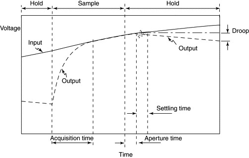
While in sample mode, the S/H' output follows its input (provided that the hold capacitor has been accurately charged and that the signal does not change too quickly). When required, the device is switched into hold mode. A short delay then ensues before digitization can commence. The delay is actually composed of two constituent delay times known as the aperture time and the settling time. The former, which is due to the internal switching time of the device, is very short, typically less than 50 ns. Variations in the aperture time, known as aperture jitter (or aperture uncertainty time), are the limiting factor in determining the temporal precision of each sample. These variations are generally on the order of 1 ns, so aperture jitter can be ignored in all but the highest-speed applications (see later for more on the relationship between aperture jitter and maximum sampling rate). The settling time is the time required for the output to stabilize after the switch and determines the rate at which samples can be obtained. It is usually on the order of 1 μs, but some systems exhibit much longer or shorter settling times.
When the output settles to a stable state, it can be digitized by the ADC. Digitization must be completed within a reasonably short time interval because the charge on the hold capacitor begins to decay, causing the S/H's output to “droop.” Droop rates vary between different devices, but are typically on the order of 1 mV/ms. Devices are available with both higher and lower droop rates. S/H circuits with low droop rates are usually required in simultaneous sample-and-hold systems. Large hold capacitors are needed to minimize droop and these can adversely affect the device's acquisition time.
5. Digitization and Signal Conversion
The PC is capable of reading and writing only digital signals. To permit interfacing of the PC to external analog systems, ADCs and DACs must be used to convert signals from analog to digital form and vice versa. This section describes the basic principles of the conversion processes. It also illustrates some of the characteristics of ADCs and DACs of which you should be aware when writing interface software.
5.1. Binary Coding
In order to understand the digitization process, it is important to consider the ways in which analog signals can be represented digitally. Computers store numbers in binary form. There are several binary coding schemes. Most positive integers, for example, are represented in true binary (sometimes called natural or straight binary). Just as the digits in a decimal number represent units, tens, hundreds, and so forth, true binary digits represent ones, twos, fours, eights, and so on. Floating-point numbers, on the other hand, are represented within the computer in a variety of different binary forms. Certain fields within the floating-point bit pattern are set aside for exponents or to represent the sign of the number. Although floating-point representations are needed to scale, linearize, and otherwise manipulate data within the PC, all digitized analog data are generally transferred in and out of the computer in the form of binary integers.
Analog signals may be either unipolar or bipolar. Unipolar signals range from zero up to some positive upper limit, while bipolar signals can span zero, varying between nonzero negative and positive limits.
5.2. Encoding Unipolar Signals
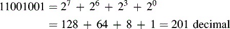
Unipolar signals are perhaps the most common and are the simplest to represent in binary form. They are generally coded as true binary numbers with which most readers should already be familiar. As mentioned previously the least significant bit has a weight (value) of 1 in this scheme, and the weight of each successive bit doubles as we move toward the most significant bit (MSB). If we allocate an index number, i, to each bit, starting with 0 for the LSB, the weight of any one bit is given by 2i. Bit 6 would, for example, represent the value 26(=64 decimal). To calculate the value represented by a complete binary number, the weights of all nonzero bits must be added. For example, the following 8-bit true binary number would be evaluated as shown. (4)
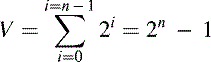
The maximum value that can be represented by a true binary number has all bits set to 1. Thus, a true binary number with n bits can represent values from 0 to V, where (5)
An 8-bit true binary number can, therefore, represent integers in the range 0 to 255 decimal (=28 – 1). A greater range can be represented by binary numbers having more bits. Similar calculations for other numbers of bits yield the results shown in Table 2. The accuracies with which each true binary number can represent an analog quantity are also shown.
Table 2. Ranges of true binary numbers
| Number of bits | Range (true binary) | Accuracy (%) |
|---|---|---|
| 6 | 0 to 63 | 1.56 |
| 8 | 0 to 225 | 0.39 |
| 10 | 0 to 1 023 | 0.098 |
| 12 | 0 to 4 095 | 0.024 |
| 14 | 0 to 16 383 | 0.0061 |
| 18 | 0 to 65 535 | 0.0015 |
The entries in this table correspond to the numbers of bits employed by typical ADCs and DACs. It should be apparent that converters with a higher resolution (number of bits) provide the potential for a greater degree of conversion accuracy.
When true binary numbers are used to represent an analog quantity, the range of that quantity should be matched to the range (i.e., V) of the ADC or DAC. This is generally accomplished by choosing a signal-conditioning gain that allows the full-scale range of a sensor to be matched exactly to the measurement range of the ADC. A similar consideration applies to the range of DAC outputs required to drive actuators. Assuming a perfect match (and that there are no digitizing errors), the limiting accuracy of any ADC or DAC system depends upon the number of bits available. An n-bit system can represent some physical quantity that varies over a range 0 to R, to a fractional accuracy ±½δ where (6)
![]()
This is equal to the value represented by one LSB. True binary numbers are important in this respect as they are the basis for measuring the resolution of an ADC or DAC.
5.2.1. Encoding Bipolar Signals
Many analog signals can take on a range of positive and negative values. It is, therefore, essential to be able to represent readings on both sides of zero as digitized binary numbers. Several different binary coding schemes can be used for this purpose. One of the most convenient and widely used is offset binary. As its name suggests, this scheme employs a true binary coding, which is simply offset from zero. This is best illustrated by an example. Consider a system in which a unipolar 0–10-V signal is represented in 12-bit true binary by the range of values from 0 to 4095. We can also represent a bipolar signal in the range −5V to +5V by using the same scaling factor (i.e., volts per bit) and simply shifting the 0-volt point halfway along the binary scale to 2048. An offset binary value of 0 would, in this case, be equivalent to −5V, and a value of 4095 would represent +5V. Offset binary codes can, of course, be used with any number of bits.
Two's complement binary can also represent both positive and negative numbers. It employs a sign bit at the MSB location. This bit is 0 for positive numbers and 1 for negative numbers. Because one bit is dedicated to storing sign information, it cannot be used for coding the absolute magnitude of the binary number and so the range of magnitudes that can be represented by two's complement numbers is half that which can be accommodated by the same number of bits in true binary. To negate a positive binary integer, it is only necessary to complement (convert zeros to ones and ones to zeros) each bit and then add 1 to the result. Carrying out this operation—which is equivalent to multiplying by −1—twice in succession yields the original number. As most readers will be aware, this scheme is used by the IBM PC's 80x86 processor for storing and manipulating signed integers because it greatly simplifies the operations required to perform subtractive arithmetic. A number of ADCs, particularly those designed for audio and digital signal processing applications, also use this coding scheme.
There are a variety of less widely used methods of coding bipolar signals. For example, a simple true binary number, indicating magnitude, may be combined with an additional bit to record the sign of the number. Another encoding scheme is one's complement (or complementary straight) binary in which negative numbers are formed by simply inverting each bit of the equivalent positive true-binary number. Combinations of these coding schemes are sometimes used. For example, complementary offset binary consists of an offset binary scale in which each code is complemented. The result is that the zero binary code (all zeros) corresponds to the positive full-scale position, while the maximum binary code (all ones) represents the negative full-scale position. Yet another scheme, complementary two's complement, is formed by simply inverting each bit of a two's complement value. These methods of binary coding are less important in PC applications although some ADCs may generate signed true binary or one's complement binary codes. Some DAC devices use the complementary offset binary scheme.
The various bipolar codes are compared in Table 3. This shows how a 3-bit binary number can represent values from −4 to +4 using the different coding schemes. The patterns shown in this table can be easily extended to numbers encoded using a greater number of bits. Note that only offset binary, complementary offset binary, and two's complement binary have a unique zero code. Note also that these schemes are asymmetric about their zero point. Compare in particular the two forms of offset binary.
Table 3. Comparison of bipolar binary codes
| Value | Offset binary | Two's complement | One's complement | Complementary offset binary |
|---|---|---|---|---|
| +3 | 111 | 011 | 011 | 000 |
| +2 | 110 | 010 | 010 | 001 |
| +1 | 101 | 001 | 001 | 010 |
| 0 | 100 | 000 | 000 or 111 | 011 |
| −1 | 011 | 111 | 110 | 100 |
| −2 | 010 | 110 | 101 | 101 |
| −3 | 001 | 101 | 100 | 110 |
| −4 | 000 | 100 | — | 111 |
Conversion from offset binary to two's complement binary is simply a matter of complementing the MSB. Complementing it again reverts back to offset binary encoding. It is a very straightforward task to convert between the various bipolar codes and examples will not be given here.
5.2.2. Other Binary Codes and Related Notations
There are two other binary codes which can be used in special circumstances: the Gray code and BCD. Both of these are, in fact, unipolar codes and cannot represent negative numbers without the addition of an extra sign bit. We have already introduced the Gray code in relation to digital encoders earlier in this chapter, but because the DA&C programmer rarely needs to use this code directly it will not be discussed further.
Binary Coded Decimal
Binary coded decimal (BCD) is simply a means of encoding individual decimal digits in binary form. Each decimal digit is coded by a group of 4 bits. Although each group would be capable of recording 16 true binary values, only the lower 10 values (i.e., corresponding to 0 to 9, decimal) are used. The remaining values are unused and are invalid in BCD. A number with N decimal digits would occupy 4N bits, arranged such that the least significant group of 4 bits would represent the least significant decimal digit. For example,
![]()
ADCs that generate BCD output are used mostly for interfacing to decimal display devices such as panel meters. Most ADCs employed in PC applications (e.g., those on plug-in DA&C cards) use one of the coding schemes described previously, such as offset binary. However, a few components of the PC do make use of BCD. For example, the 16-bit 8254 timer counter used on AT compatible machines and on some plug-in data-acquisition cards can operate in a four-decade BCD mode.
Hexadecimal Notation
This is not a binary code. It is, in fact, a base-16 (rather than base-2) numeric representation. Hexadecimal notation is rather like BCD in that 4 bits are required for each hexadecimal digit. However, all 16 binary codes are valid and so each hexadecimal digit can represent the numbers from 0 to 15 (decimal). Hexadecimal numbers are written using an alphanumeric notation in which the lowest 10 digits are represented by 0 to 9 and the remaining digits are written using the letters A to F. A corresponds to 10 decimal, B to 11, and so on. Hexadecimal numbers are followed by an h to avoid confusing them with decimal numbers. The following example shows the binary and decimal equivalents of a 2-digit hexadecimal number:
![]()
Most numbers manipulated by computer software are coded using multiples of 4 bits: usually either 8, 16, or 32 bits. Hexadecimal is, therefore, a convenient shorthand method for expressing binary numbers and is used extensively in this and other publications.
5.2.3. Digital-to-Analog Converters
Digital-to-analog converters (DACs) have a variety of uses within PC-based DA&C systems. They may be used for waveform synthesis, to control the speed of DC motors or to drive analog chart recorders and meters. Many closed-loop control systems require analog feedback from the PC and this is invariably provided by a DAC.
Most DACs generate full-scale outputs of a few volts (typically 0–10V, ±5V, or ±10V). They have a limited current-driving capability (usually less than about 1–10 mA) and are often buffered using operational amplifiers. In cases where a low-impedance or high-power unit is to be driven, suitable power amplifiers may be required. Current-loop DACs with full-scale outputs of 4–20 mA are also available and these are particularly suited to long-distance transmission in noisy environments. Both bipolar and unipolar configurations are possible on many proprietary DAC cards by adjusting jumpers or DIP switches.
The resolution of a DAC is an important consideration. This is the number of input bits that the DAC can accept. As Equation (5) shows, it determines the accuracy with which the device can reconstruct analog signals. The 8-bit and 12-bit DACs are, perhaps, the most common in DA&C applications although devices with a variety of other resolutions are available. Figure 9 shows the ideal transfer characteristic of a DAC. For reasons of clarity, this illustration is based on a hypothetical 3-bit DAC, having eight possible codes from 000b to 111b. Note that, although there are eight codes, the DAC can only generate an output accurate to one seventh of its maximum output voltage, which is one LSB short of its nominal full-scale value, Vmax.
Figure 9. Ideal DAC transfer characteristic (unipolar true binary encoding).
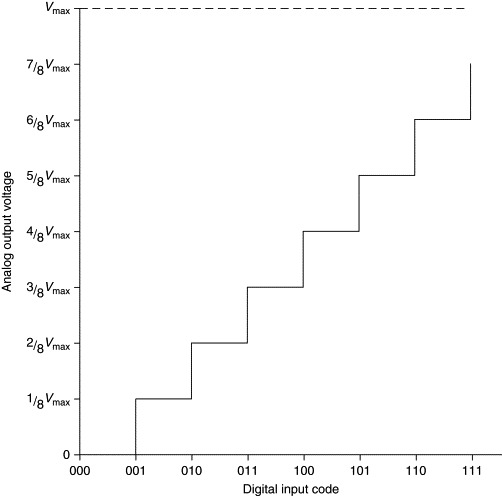
DACs are generally controlled via registers mapped to one or more of the PC's I/O ports. When the desired bit pattern is written to the register, the DAC updates its analog output accordingly. If a DAC has more than 8 bits, it requires its digital input to be supplied either as one 16-bit word or as two 8-bit bytes. The latter often involves a two-stage write operation: The least significant byte is usually written first and this is followed by the most significant byte. Any unused bits (e.g., the upper 4 bits in the case of a 12-bit DAC) are ignored. The two-stage method of supplying new data can sometimes cause problems if the DAC's output is updated immediately upon receipt of each byte. Spurious transients can be generated because the least significant byte of the new data is initially combined with the most significant byte of the existing data. The analog output settles to its desired value only when both new bytes have been supplied. To circumvent this problem, many DACs incorporate a double buffering system in which the first byte is held in a buffer until the second byte is received, at which point the complete control word is transferred to the DAC's signal-generating circuitry.
Most devices employ a network of resistors and electronic switches connected to the input of an operational amplifier. The network is arranged such that each switch and its associated resistors make a binary-weighted contribution to the output of the amplifier. Each bit of the digital input operates one of the switches and thereby controls the input to, and output from, the amplifier. The operational amplifier and resistor network function basically as a multiplier circuit. It multiplies the digital input (expressed as a fraction of the full-scale digital input) by a fixed reference voltage. The reference voltage may be supplied by components external to the DAC. Most plug-in DA&C cards for the PC include suitable precision voltage references. Some also provide the facility for users to connect their own reference voltage and thereby to adjust the full-scale range of the DAC. Further details of DAC operation may be found in the texts by Tompkins and Webster (1988) and Vears (1990).
The output of a DAC can usually be updated quite rapidly. Each bit transition gives rise to transient fluctuations which require a short time to settle. The total settling time depends upon the number of bits that change during the update and is greatest when all input bits change (i.e., for a full-scale swing). The settling time may be defined as the time required after a full-scale input step for the DAC's output to settle to within a negligibly small band about its final level. The term negligibly small has to be defined. Some DAC manufacturers define it as “within ±½ LSB,” while others define it as a percentage of full scale, such as ±0.001%. Quoted settling times range from about 0.1 to 150 μs, and sometimes up to about 1 ms, depending upon the characteristics of the device and on how the settling time is defined. Most DACs, however, have settling times on the order of 5–30 μs. In practice the overall settling time of an analog output channel may be affected by external power amplifiers and other components connected to the DAC's outputs. You are advised to consult manufacturers' literature for precise timing specifications.
5.2.4. Characteristics of DACs
Because of small mismatches in components (e.g., the resistor network), it is not generally possible to fabricate DACs with the ideal transfer characteristic illustrated in Figure 9. Most DACs deviate slightly from the ideal, exhibiting several types of imperfection as shown in Figure 10. You should be aware of these potential sources of error in DAC outputs, some of which can be corrected by the use of appropriate software techniques.
Figure 10. Nonideal DAC transfer characteristics: (A) gain and offset errors and (B) nonlinearity and nonmonotonicity.
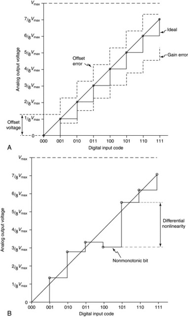
The transfer characteristic may be translated along the analog-output axis giving rise to a small offset voltage. Incorrect gains will modify the slope of the transfer characteristic such that the desired full-scale output is either obtained with a binary code lower than the ideal full-scale code (all ones) or never reached at all. Gain errors equivalent to a few LSB are typical.
Linearity is a measure of how closely the output conforms to a straight line drawn between the end points of the conversion range. Linearity errors, which are due to small mismatches in the resistor network, cause the output obtained with some binary codes to deviate from the ideal straight-line characteristic. Most modern monolithic DACs are linear to within ±1 LSB or less. Differential nonlinearity is the maximum change in analog output occurring between any two adjacent input codes. It is defined in terms of the variation from the ideal step size of 1 LSB. Differential nonlinearities are usually on the order of ±1 LSB or less. If nonlinearity is such that the output from the DAC fails to increase over any single step in its input, the DAC is said to be nonmonotonic. Monotonicity of a DAC is usually expressed as the number of bits over which monotonicity is maintained. If a DAC has a nonlinearity better than ±½ LSB, then it must be monotonic (it cannot be nonmonotonic, by definition).
Although one can often compensate for gain and offset errors by manual trimming, it is not possible to correct nonlinear or nonmonotonic DACs—these characteristics are intrinsic properties of the device. Fortunately, most modern DAC designs yield quite small nonlinearities which can usually be ignored.
5.3. Analog-to-Digital Converters
An analog-to-digital converter (ADC) is required to convert analog sensor signals into a binary form suitable for reading into the PC. A wide variety of ADCs are available for this platform, either on plug-in DA&C cards or within remote signal-conditioning units or data loggers. This section introduces the basic concepts involved in analog-to-digital conversion and describes some of the properties of ADCs that are relevant to the design of DA&C software.
5.3.1. Resolution and Quantization Error
It should be apparent to the reader that, because of the discrete nature of digital signals, some analog information is lost in the conversion process. A small but finite range of analog input values are capable of generating any one digital output code. This range is known as the code width or, more properly, as a quantum as it represents the smallest change in analog input that can be represented by the system. Its size corresponds to 1 LSB. The uncertainty introduced as a result of rounding to the nearest binary code is known as quantization error and has a magnitude equal to ±½ LSB. Obviously, the quantization error is less important relative to the full-scale input range in ADCs that are capable of generating a wider range of output codes (i.e., those with a greater number of bits).
Some devices have a relatively low resolution of 8 bits or less, while others, designed for more precise measurements, may have 12 or 16 bits. ADCs usually have full-scale input ranges of a few volts: typically 0–10V (unipolar) or ±5V (bipolar). The quantization error is thus on the order of a few millivolts. Precise figures can easily be calculated by applying Equation (6), knowing the device's input range and resolution, as shown in the following example.
Consider a 12-bit ADC system designed for monitoring the displacement of some object using an LVDT over a range 0 to 50 mm. If the full analog range is encompassed exactly by the available digital codes, then we can calculate the magnitude of the LSB from Equation (6):
![]()
In this example, the quantization error imposes an accuracy of ±½δr = ±0.006 mm. This presupposes that we use the whole range of available ADC codes. The effective quantization error is clearly worse if only part of the ADC's digitizing range is used. The quantization error indicates the degree of precision that can be attained in an ideal device. It is not, however, representative of the overall accuracy of most real ADCs. We will discuss other sources of inaccuracy later in this chapter.
5.3.2. Quantization Noise
For a data acquisition system equipped with an n-bit ADC and designed to measure signals over a range R, we have seen that the quantization error is ±Q, where Q = ½δR. The difference between an analog value and its digitized representation appears as a varying noise signal superimposed upon the true analog signal. The amplitude of the noise signal varies by an amount determined by the magnitude of the quantization error and, if the signal to be digitized consists of a pure sine wave of amplitude ±½R, the root-mean-square value of the noise component is given by (7)
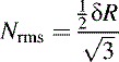 which, when we substitute for δR, gives (8)
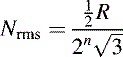
The rms value of the signal itself is (9)
 so the ratio of the rms signal to rms noise values—the signal-to-noise ratio, SNR—is given by (10)
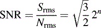
It is normal to express SNR in decibels, where SNRdB = 20 log (SNR). This gives the approximate relationship: (11)
![]()
This equation relates the number of bits to the dynamic range of the ADC—that is, the signal-to-noise ratio inherent in digitization. Conversely, in a real measuring system, where other sources of noise are present, Equation (11) can be used to determine the number of ADC bits that will encode signal changes above the ambient noise level. The contribution made by the low-order bits of an ADC may be considerably less than the rms level of noise introduced by other system components. For example, differential and integral nonlinearities inherent in the ADC, electronic pickup, sensor noise, and unwanted fluctuations in the measurand itself may also degrade the SNR of the system as a whole. In many systems the SNR is limited to around 75 to 85 dB by these factors. Where large noise amplitudes are present, it is fruitless to employ a very high-resolution ADC. It may, in such cases, be possible to use an ADC with a lower resolution (and hence lower SNRdB) without losing any useful information. Later we present some simple techniques for removing unwanted noise from digitized signals.
5.3.3. Conversion Time
Most types of ADC use a multiple-stage conversion process. Each stage might involve incrementing a counter or comparing the analog signal to some digitally generated approximation. Consequently, analog-to-digital conversion does not occur instantaneously. Depending upon the method of conversion used, times ranging from a few microseconds up to several seconds may be required. Conversion times are generally quoted in manufacturer's data sheets as the time required to convert a full-scale input. Some devices (such as binary-counter-type ADCs) are capable of converting lower-level signals in a shorter time. In general, low-resolution devices tend to be faster than high-resolution ADCs. The fastest 16- bit ADCs currently have conversion times of about 1 ms. As a rough rule of thumb, the conversion time of the fastest devices currently available tends to increase by roughly an order of magnitude for every additional 2 bits resolution. The conversion times applicable to the various types of ADC are described in the following section.
5.3.4. Types of ADC
There are several basic classes of ADC. The different conversion techniques employed make each type particularly suited to certain types of application. Some ADCs are implemented by using a combination of discrete components (counters, DACs, etc.) in conjunction with controlling software. This approach is particularly suited to producing very high-resolution converters. However, it tends to be used less often in recent years as high resolution and reasonably priced monolithic ADCs are now becoming increasingly available. The various types of ADC are described next in approximate order of speed: the slowest first.
Voltage-to-Frequency Conversion ADCs
This type of ADC employs a voltage-to-frequency converter (VFC) to transform the input signal into a sequence of digital pulses. The frequency of the pulse train is proportional to the input voltage. A binary counter counts the pulses over a fixed time interval and the total accumulated count provides the ADC's digital output. The time period over which the pulses are counted varies with the required resolution and full-scale frequency of the VFC. Typical conversion times range from about 50 ms up to several seconds.
Because the input voltage is effectively averaged over the conversion period, VFC-based ADCs exhibit good noise immunity. However, their slow response restricts them to low-speed sampling applications. This type of ADC is inherently monotonic, but linearities and gain errors can be variable. Devices based on lower-frequency (10 kHz) VFCs tend to be more accurate than those employing high-speed VFCs.
VFCs are sometimes used to digitize analog signals at remote sensing locations. The advantage of this approach is that sensor signals can be more easily transmitted in digital form over long distances or through noisy environments. The digital pulse train is received by the PC or data-logging unit and then processed using a suitable counter. The resolution and speed of such a system can easily be modified under software control by reprogramming the counter and timer hardware accordingly.
5.3.5. Dual-Slope (Integrating) ADCs
Dual-slope ADCs each employ a binary counter in conjunction with an integrating circuit that sums the input signal over a fixed time period as shown in Figure 11. The rate of increase of the integral during this time is proportional to the average input signal. When the integration has been completed, a negative analog reference voltage is applied to the integrating circuit and the timer is started. The combined integral of the two inputs then falls linearly. The time taken for the integral to fall to zero is directly proportional to the average input voltage. The binary output from the timer is then used to provide the ADC's digital output.
Figure 11. Signal integration in a dual-slope ADC.
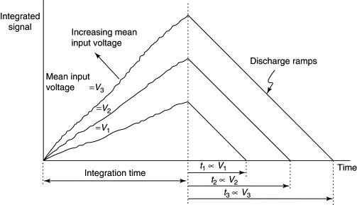
Because the input signal is integrated over time, this type of ADC averages out signal variations due to noise and other sources. Typical integration times are usually on the order of a few milliseconds or longer, limiting the sample rate to typically 5–50 Hz. Dual-slope ADCs are particularly suited to use in noisy environments and are often capable of rejecting mains-induced noise. For this reason, they are popular in low-speed sampling applications such as temperature measurement. Dual-slope ADCs are relatively inexpensive, offer good accuracy and linearity, and can provide resolutions of typically 12 to 16 bits.
The related single-slope (or Wilkinson) technique involves measuring the time required to discharge a capacitor that initially holds a charge proportional to the input signal. In this case, the capacitor may be a component of circuitry used for signal conditioning or pulse shaping. This technique is sometimes used in conjunction with nuclear radiation detectors for pulse-height analysis in systems designed for X-ray or gamma-ray spectrometry.
Binary Counter ADCs
This type of ADC also employs a binary counter, but in this case it is connected to the input of a DAC. The counter is supplied with a clock input of fixed frequency. As the counter is incremented it causes the analog output from the DAC to increase as shown in Figure 12(A). This output is compared with the signal to be digitized and, as soon as the DAC's output reaches the level of the input signal, the counter is stopped. The contents of the counter then provide the ADC's digital output. The accuracy of this type of converter depends upon the precision of the DAC and the constancy of the clock input. The binary counting technique provides moderately good resolution and accuracy, although conversion times can be quite long, particularly for inputs close to the upper end of the device's measuring range. This limits throughput to less than a few hundred samples per second.
Figure 12. DAC output generated by (A) binary counter ADCs and (B) tracking ADCs.
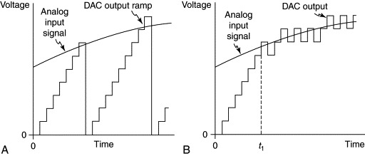
The main disadvantage with this type of converter is that the conversion time varies with the magnitude of the input signal. A variant of the simple binary counter method, known as the tracking converter, provides a solution to this problem and also allows higher sampling rates to be used. The tracking converter continuously follows the analog input, ramping its DAC output up or down to maintain a match between its digital output and the analog input as shown in Figure 12(B). The software may, at any time after t1, stop the tracking (which temporarily freezes the digital output) and then read the ADC. After an initial conversion has been performed, subsequent conversions only require enough time to count up or down to match any (small) change in the input signal. This method operates at a somewhat faster (and less variable) speed than the simple binary counter ADC.
Successive Approximation ADCs
The successive approximation technique makes use of a DAC to convert a series of digital approximations of the input signal into analogue voltages. These are then compared with the input signal. The approximations are applied in a binary-weighted sequence as shown in Figure 13 which, for the sake of clarity, shows only a 4-bit successive approximation sequence. However, 8 to 16 bits are more typical of actual ADC implementations.
Figure 13. DAC output generated during successive approximation.
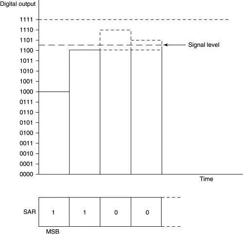
A reference voltage corresponding to the ADC's MSB is generated first. If this is less than the input signal, a 1 bit is stored in the MSB position of an internal successive approximation register (SAR), otherwise a 0 is stored. Each subsequent approximation involves generating a voltage equivalent to all of the bits in the SAR that have so far been set to 1, plus the value of the next bit in the sequence. Again, if the total voltage is less than the input signal, a 1 value is stored in the appropriate bit position of the SAR. The process repeats, for bits of lesser significance until the LSB has been compared. The SAR will then contain a binary approximation of the analog input signal.
Because this process involves only a small number of iterations (equal to the number of bits), successive approximation ADCs can operate relatively quickly. Typical conversion times are on the order of 5–30 μs. Successive approximation ADCs offer between 8- and 16-bit resolutions and exhibit a moderately high degree of linearity. This type of ADC is widely used in PC interfacing applications for data acquisition at rates up to 100 kHz. Many manufacturers provide inexpensive general-purpose DA&C cards based on successive approximation ADCs.
Unlike some other types of ADC, the process of successive approximation does not involve an inherent averaging of the input signal. The main characteristic of these devices is their high operating speed rather than noise immunity. To fully utilize this high-speed sampling capability, the ADC's input must remain constant during the conversion. Many ADC cards employ onboard S/H circuits to freeze the input until the conversion has been completed. Some monolithic successive approximation ADCs include built-in S/H circuits for this purpose. In these cases the total conversion time specified in manufacturer's data sheets may include the acquisition time of the S/H circuit.
Parallel (Flash) ADCs
This is the fastest type of ADC and is normally used in only very high-speed applications, such as in video systems. It employs a network of resistors that generate a binary-weighted array of reference voltages. One reference voltage is required for each bit in the ADC's digital output. A comparator is also assigned to each bit. Each reference voltage is applied to the appropriate comparator, along with a sample of the analog input signal. If the signal is higher than the comparator's reference voltage, a logical 1 bit is generated, otherwise the comparator outputs a logic 0.
In this way the signal level is simultaneously compared with each of the reference voltages. This parallel digitization technique allows conversions to be performed at extremely high speed. Conversion times may be as low as a few nanoseconds, but more typically fall within the range 50–1000 ns. Parallel converters require multiple comparators and this means that high resolution devices are difficult and expensive to fabricate. Resolutions are consequently limited to 8 to 10 bits or less. Greater resolutions can sometimes be achieved by cascading two flash converters. Some pseudo-parallel converters, known as subranging converters, employ a half flash technique in which the signal is digitized in two stages (typically within about 1 ms). The first stage digitizes the most significant bits in parallel. The second stage digitizes the least significant bits.
5.3.6. Using ADCs
As well as their analogue input and digital output lines, most monolithic ADCs have two additional digital connections. One of these, the start conversion (also sometimes known as the SC or START) pin, initiates the analog-to-digital conversion process. Upon receiving the SC signal, the ADC responds by deactivating its end of conversion (EOC) pin and then, when the conversion process has been completed, it asserts EOC once more. The processor should sense the EOC signal and then read the digitized data from the ADC's output register.
On plug-in DA&C cards, the SC and EOC pins are generally mapped to separate bits within one of the PC's I/O ports and can thus be controlled and sensed using assembly language IN and OUT instructions. The ADC's output register is also normally mapped into the PC's I/O space. In contrast, stand-alone data logging units and other intelligent instruments may initiate and control analog-to-digital conversion according to preprogrammed sequences. In these cases ADC control is reduced to simply issuing the appropriate high-level commands from the PC.
As an alternative to software initiation, some systems allow the SC pin to be controlled by onboard components such as counters, timers, or logic level control lines. Some ADC cards include a provision for the EOC signal to drive one of the PC's interrupt request lines. Such systems allow the PC's software to start the conversion process and then to continue with other tasks rather than waiting for the ADC to digitize its input. When the conversion is complete the ADC asserts EOC, invoking a software interrupt routine that then reads the digitized data.
Most ADC cards will incorporate I/O-mapped registers that control not just the ADC's SC line, but will also operate an onboard multiplexer and S/H circuit (if present) as shown in Figure 14. The details of the register mapping and control-line usage vary between different systems, but most employ facilities similar to those just described. Often the S/H circuit on the input to the ADC is operated automatically when the SC line is asserted. It should be noted, however, that simultaneous S/H circuits are generally operated independently of the ADC via separate control lines. You should consult your system's technical documentation for precise operational details.
Figure 14. A typical multiplexed ADC card.
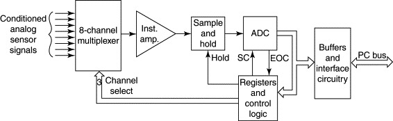
5.4. ADC Characteristics and Errors
Figure 15 illustrates the characteristics of an ideal ADC. For the sake of clarity, the output from a hypothetical 3-bit ADC is shown. The voltage supplied to the ADC's input is expressed as a fraction of the full-scale input, FS.
Figure 15. Transfer characteristic of an ideal ADC.
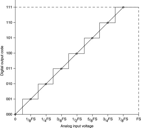
Note that each digital code can represent a range of analog values known as the code width. The analog value represented by each binary code falls at the midpoint of the range of values encompassed by that code. These midrange points lie on a straight line passing through the origin of the graph as indicated in the figure. Consequently the origin lies at the midrange point of the lowest quantum. In this illustration, a change in input equivalent to only ½ LSB will cause the ADC's output to change from 000b to 001b. Because of the positions of the zero and full-scale points, only 2n – 1 (rather than 2n) changes in output code occur for a full-scale input swing.
Like DACs, analog-to-digital converters exhibit several forms of nonideal behaviour. This often manifests itself as a gain error, offset error, or nonlinearity. Offset and gain errors present in ADCs are analogous to the corresponding errors already described for DACs. These are illustrated in Figure 16 which, for the sake of clarity, shows only the center points of each code. ADC gain errors can be caused by instabilities in the ADC's analog reference voltage or by gain errors in their constituent DACs. Gain and offset errors in most monolithic ADCs are very small and can often be ignored.
Figure 16. Errors in ADC transfer characteristics.
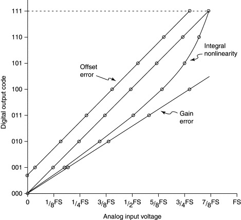
ADCs may have missing codes—that is, they may be incapable of generating some codes between the end points of their measuring range. This occurs if the DAC used within the ADC is nonmonotonic. Nonlinearity (sometimes referred to as integral nonlinearity) is a measure of the maximum deviation of the actual transfer characteristic from the ideal response curve. Nonlinearities are usually quoted as a fraction of the LSB. If an ADC has a nonlinearity of less than ½ LSB then there is no possibility that it will have missing codes.
Differential nonlinearity is the maximum difference between the input values required to produce any two consecutive changes in the digital output—that is, the maximum deviation of the code width from its ideal value of 1 LSB. Nonlinearities often occur when several bits all change together (e.g., as in the transition from 255 to 256) and because of this they tend to follow a repeated pattern throughout the converter's range.
The overall accuracy of an ADC will be determined by the sum total of the deviations from the ideal characteristic introduced by gain errors, offset errors, nonlinearities, and missing codes. These errors are generally temperature dependent. Gain and offset errors can sometimes be trimmed or removed, but nonlinearities and missing codes cannot be easily compensated for. Accuracy figures are often quoted in ADC data sheets. They are usually expressed as a percentage of full-scale input range or in terms of the analog equivalent of the LSB step size. Typical accuracy figures for 12-bit monolithic ADCs are generally on the order of ±½ to ±1 LSB. However, these figures maybe significantly worse (perhaps 4 to 8 LSB in some cases) at the extremes of the ADC's working temperature range. You are advised to study carefully manufacturers' literature in order to determine the operational characteristics of the ADC in your own system.
6. Analog Measurements
In this section we will discuss three topics of particular importance in the design of analog measuring systems: accuracy, amplification, and throughput.
6.1. Accuracy
The accuracy of the whole measuring system will be determined, not just by the precision of the ADC, but also by the accuracy and linearity of the sensor and signal-conditioning circuits used. Random or periodic noise will also affect the measurement accuracy, introducing either statistically random or systematic uncertainties. The inaccuracies inherent in each component of the system (e.g., sensor instabilities, amplifier gain errors, S/H accuracy, ADC quantization error, and linearity) should be carefully assessed and summed with the expected (or measured) noise levels in order to arrive at the total potential error. A simple arithmetic sum will provide an estimate of the maximum possible error. However, in some measurements, the errors might be combined such that they oppose each other and tend to cancel out. A figure more representative of the average error that is likely to occur—that is, the statistical root-sum-square (rss) error—can be obtained by adding the individual errors in quadrature, as follows: (12)

Here, ϵ is the rss error (equivalent to the standard deviation of many readings of a fixed input), j is the number of sources of error and δk is the kth source of error expressed either in terms of the units of the measurand or as a fraction of the full-scale measurement range. To simplify the calculation δk contributions of less than about one quarter of the maximum δk can usually be ignored without significantly affecting the result. Typical errors introduced by S/H, multiplexer, and amplifiers (assuming that they are allowed to settle adequately) are often on the order of ±0.01% of full scale, or less. This may be a significant source of error, particularly in high-resolution systems (i.e., those using ADCs of greater than 10 bits resolution).
6.2. Amplification and Extending Dynamic Range
The conversion accuracy of an ADC is ultimately limited by the device's resolution. Unless the range of signal levels generated by the signal-conditioning circuitry is accurately matched to the ADC's full-scale range (typically up to 5 or 10V), a proportion of the available conversion codes will be unused. In order to take full advantage of the available resolution it is necessary to scale the signal by means of suitable amplifying components. This can easily be accommodated using fixed gain operational amplifiers or instrumentation amplifiers. Many proprietary PC data acquisition cards incorporate amplifiers of this kind. The gain can generally be selected by means of jumpers or DIP switches when the device is installed in the PC. This approach is ideal if the system is intended to measure some signal over a fixed range to a predetermined degree of accuracy.
However, many sensors have wide dynamic ranges. LVDT displacement sensors, for example, have a theoretically infinite resolution. With suitable signal conditioning they can be used to measure displacements either over their full-scale range or just over a very small proportion of their range. To measure displacements to the same fractional accuracy over full or partial ranges, it is necessary to dynamically vary the gain of the signal-conditioning circuit. This is generally accomplished by means of programmable-gain amplifiers.
The gain of a PGA can be selected, from a set of fixed values, under software control. In the case of plug-in ADC cards, gain selection is usually effected by writing a suitable bit pattern via an I/O port to one of the card's control registers. It is possible to maximize the dynamic range of the system by selecting an appropriate PGA gain setting.
The software must, of course, compensate for changes in gain by scaling the digitized readings appropriately. Binary gain ranges (e.g., 1×, 2×, 4×, 8×, etc.) are the simplest to accommodate in the software since, to reflect the gain range used, the digitized values obtained with the lowest gains can be simply shifted left (i.e., multiplied) within the processor's registers by an appropriate number of bits. If systems with other gain ranges are used, it becomes necessary to employ floating-point arithmetic to adjust the scaling factors.
Amplifiers may produce a nonzero voltage (known as an offset voltage) when a 0-V input is applied. This can be cancelled by using appropriate trimming components. However, these components can be the source of additional errors and instabilities (such as temperature-dependent drifts) and, because of this, a higher degree of stability can sometimes be obtained by canceling the offset purely in software. Offsets can also arise from a variety of other sources within the sensor and signal-conditioning circuits. It can be very convenient to compensate for all of these sources in one operation by configuring the software to measure the total offset and to subtract it from each subsequent reading. If you adopt this approach, you should bear in mind that the input to a PGA from previous amplification stages or signal-conditioning components still possesses a nonzero offset. Changing the gain of the PGA can also affect the magnitude of offset presented to the ADC. It is, therefore, prudent for the software to rezero such systems whenever the PGA's gain is changed.
One of the most useful capabilities offered by PGAs is autoranging. This permits the optimum gain range to be selected even if the present signal level is unknown. An initial measurement of the signal is obtained using the lowest (e.g., 1×) gain range. The gain required to give the optimum resolution is then calculated by dividing the ADC's resolution (e.g., 4096 in the case of a 12-bit converter) by the initial reading. The gain range less than or equal to the optimum gain is then selected for the final reading. This technique obviously reduces throughput as it involves twice as many analog-to-digital conversions and repeated gain changes.
6.3. Throughput
The throughput of an analog measuring system is the rate at which the software can sample analog input channels and process the acquired data. It is more conveniently expressed as the number of channels read per second. The distinction between this and the rate at which multiplexed groups of sensor channels can be scanned should be obvious to the reader. A system scanning a group of eight sensor channels 50 times per second will have a throughput figure of 400 channels per second.
A number of factors affect throughput. One of the most important of these is the ADC's conversion time, although it is by no means the only consideration. The acquisition time of the S/H circuit, the settling times of the multiplexer, S/H, PGA and other components, the bandwidth of filters, and the time constant of the sensor may all have to be taken into account. Each component must be fast enough to support the required throughput.
When scanning multiple channels, throughput can sometimes be maximized by changing the multiplexer channel as soon as the S/H circuit is switched into hold mode. This allows analog-to-digital conversion to proceed while the multiplexer's output settles to the level of the next input channel. This technique, known as overlap multiplexing, requires well-designed DA&C hardware to avoid feedthrough between the two channels. Compare this with the usual (slower) technique of serial multiplexing, where each channel is selected, sampled, and digitized in sequence.
Throughput is, of course, also limited by the software used. Unless special software and hardware techniques, such as direct memory access (DMA), are employed, each read operation will involve the processor executing a sequence of IN and OUT instructions. These are needed in order to operate the multiplexer (and possibly S/H), to initiate the conversion, check for the EOC signal, read 1 or 2 bytes of data, and then to store that data in memory. The time required will vary between different types of PC, but on a moderately powered system, these operations will generally introduce delays of several tens of microseconds per channel. Provided that no other software processing is required, a fast (e.g., successive approximation) ADC is used, and that the bandwidth of the signal-conditioning circuitry does not limit throughput, a well-designed 80486-based data acquisition system might be capable of reading several thousand channels per second. Systems optimized for high-speed sampling of single channels can achieve throughput rates in excess of 10,000–20,000 samples per second.
Most systems, however, require a degree of additional real-time processing. The overheads involved in scaling or linearizing the acquired data or in executing control algorithms will generally reduce the maximum attainable throughput by an order of magnitude or more. Certain operations, such as updating graphical displays or writing data to disk can take a long (and possibly indeterminate) time. The time needed to update a screen display, for example, ranges from a few milliseconds up to several hundred milliseconds (or even several seconds), depending upon the complexity of the output. Speed can sometimes be improved by coding the time-critical routines in assembly language rather than in C, Pascal, or other high-level languages.
In assessing the speed limitations that are likely to be imposed by software, it is wise to perform thorough timing tests on each routine that you intend to use during the data acquisition period. In many cases, raw data can be temporarily buffered in memory for subsequent processing during a less time-critical portion of the program. By carrying out a detailed assessment of the timing penalties associated with each software operation, you should be able to achieve an optimum distribution of functionality between the real-time and postacquisition portions of the program.
7. Timers and Pacing
Most real-time applications require sensor readings to be taken at precise times in the data acquisition cycle. In some cases, the time at which an event occurs, or the time between successive events, can be of greater importance than the attributes of the event itself. The ability to pace a data acquisition sequence is clearly important for accurately maintaining sampling rates and for correct operation of digital filters, PID algorithms, and time-dependent (e.g., chart recorder) displays. A precise time base is also necessary for measurement of frequency, for differentiating and integrating sensor inputs, and for driving stepper motors and other external equipment.
Timing tasks can be carried out by using counters on an adaptor card inserted into one of the PC's expansion slots. Indeed many analog I/O cards have dedicated timing and counting circuitry, which can be used to trigger samples, to interrupt the PC, to control the acquisition of a preprogrammed number of readings, or to generate waveforms.
Another approach to measuring elapsed time is to use the timing facilities provided by the PC. This is a relatively easy task when programming in a real-mode environment (e.g., DOS). It becomes more complex, however, under multitasking operating systems such as Windows NT or OS/2, where one has limited access to and less control over, the PC's timing hardware. The PC is equipped with a programmable system clock based on the Intel 8254 timer counter, as well as a Motorola MC146818A real time clock (RTC) IC. These, together with a number of BIOS services provide real-mode programs with a wealth of timing and calendrical features.
Whatever timing technique is adopted, it is important to consider the granularity of the timing hardware—that is, the smallest increment in time that it can measure. This should be apparent from the specification of the timing device used. The PC's system timer normally has a granularity of about 55 ms and so (unless it is reprogrammed accordingly) it is not suitable for measuring very short time intervals. The RTC provides a periodic timing signal with a finer granularity, approximately 976 μs. There are various software techniques that can yield granularities down to less than 1 ms using the PC's hardware, although such precise timing is limited in practice by variations in execution time of the code used to read the timer. The texts by (van Gilluwe 1994) and (Sanchez and Canton 1994) provide useful information for those readers wishing to exploit the timing capabilities of the PC.
When devising and using any timing system that interacts with data acquisition software (as opposed to a hardware-only system), it must be borne in mind that the accuracy of time measurements will be determined, to a great extent, by how the timing code is implemented. As in many other situations, assembly language provides greater potential for precision than a high-level language. A compiled language such as C or Pascal is often adequate for situations where timing accuracies on the order of 1 ms are required.
Most programming languages and development environments include a variety of time-related library functions. For example, National Instruments' LabWindows/CVI (an environment and library designed for creating data acquisition programs) when running on Windows NT supplies the application program with a timing signal every 1 ms or 10 ms (depending upon configuration). A range of elapsed-time, time-delay, and time-of-day functions is also provided.
7.1. Watchdog Timers
In many data-acquisition applications the PC must communicate with some external entity such as an intelligent data-logging module or a programmable logic controller. In these cases it can be useful for both components of the system to be “aware” of whether the other is functioning correctly. There are a number of ways in which the state of one subsystem can be determined by another. A program running on a PC can close a normally open contact to indicate that it has booted successfully and is currently monitoring some process or other. If the PC and relay subsequently lose power, the contact will open and alert external equipment or the operator to the situation. However, suppose that power to the PC remained uninterrupted, but the software failed due to a coding error or memory corruption. The contact would remain closed even though the PC was no longer functional. The system could not then make any attempt to automatically recover from the situation. Problems like this are potentially expensive, especially in long-term data-logging applications where the computer may be left unattended and any system crash could result in the loss of many days' worth of data.
A watchdog timer can help to overcome these problems. This is a simple analog or digital device that is used to monitor the state of one of the component parts of a data acquisition or computer system. The subsystem being monitored is required to refresh the watchdog timer periodically. This is usually done by regularly pulsing or changing the state of a digital input to the watchdog timer. In some implementations the watchdog generates a periodic timing signal and the subsystem being monitored must then refresh the watchdog within a predetermined interval after receipt of this signal. If the watchdog is not refreshed within a specified time period it will generate a timeout signal. This signal can be used to reset the subsystem or it can be used for communicating the timeout condition to other subsystems.
The IBM PS/2 range of computers is equipped with a watchdog timer that monitors the computer's system timer interrupt (IRQ0). If the software fails to service the interrupt, the watchdog generates an NMI.
It is worth mentioning at this point that you should avoid placing watchdog-refresh routines within a hardware-generated periodic interrupt handler (e.g., the system timer interrupt). In the event of a software failure, it is possible that the interrupt will continue to be generated at the normal rate!
It is sometimes necessary to interface a watchdog timer to a PC-based data acquisition system in order to detect program crashes or loss of power to the PC. The timeout signal might be fed to a programmable logic controller, for example, to notify it (or the operator) of the error condition. It is also possible to reboot the PC by connecting the timeout signal to the reset switch (present on most PC-compatible machines) via a suitable relay and/or logic circuits. Occasionally, software crashes can (depending upon the operating system) leave the PC's support circuits in such a state of disarray that even a hardware reset cannot reboot the computer. The only solution in this case is to temporarily turn off the computer's power. Although rebooting via the reset switch might be possible, the process can take up to two or three minutes on some PCs. It is not always easy for the software to completely recover from this type of failure, especially if the program crash or loss of power occurred at some critical time such as during a disk-write operation. It is preferable for the software to attempt to return to a default operating mode and not to rely on any settings or other information recorded on disk. The extent to which this is feasible will depend upon the nature and complexity of the application.
8. Sampling, Noise, and Filtering
Virtually all data acquisition and control systems are required to sample analog waveforms. The timing of these samples is often critical and has a direct bearing on the system's ability to accurately reconstruct and process analog signals. The rest of this chapter introduces elements of sampling theory and discusses how measurement accuracy is related to signal frequency and to the temporal precision of the sampling hardware. The associated topic of digital filtering is also discussed.
9. Sampling and Aliasing
Analog signals from sensors or transducers are continuous functions, possessing definite values at every instant of time. We have already seen that the PC can read only digitized representations of a signal and that the digitization process takes a finite time. Implicit in our discussion has been the fact that the measuring system is able to obtain only discrete samples of the continuous signal. It remains unaware of the variation of the signal between samples.
9.1. The Importance of Sampling Rate
We can consider each sample to be a digital representation of the signal at some fixed point in time. In fact, the readings are not truly instantaneous but, if suitable sample-and-hold circuits are used, each reading is normally representative of a very well-defined instant in time (typically accurate to a few nanoseconds).
In general, the sampling process must be undertaken in such a way as to minimize the loss of time-varying information. It is important to take samples at a sufficiently high rate in order to be able to accurately reconstruct and process the signal. It should be obvious that a system which employs too low a sampling rate will be incapable of responding to rapid changes in the measurand. Such a situation is illustrated in Figure 17. At low sampling rates, the signal is poorly reconstructed. High-frequency components such as those predominating between sample times t4 and t6 are most badly represented by the sampled points. This can have serious consequences, particularly in systems that have to control some process. The inability to respond to transient disturbances in the measurand may compromise the system' ability to maintain the process within required tolerances.
Figure 17. Degradation of a reconstructed signal as the sampling rate is reduced.
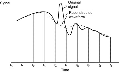
Clearly, the relationship between the sampling rate and the maximum frequency component of the signal is of prime importance. There are normally a number of practical limitations on the maximum sampling frequency that can be achieved; for example, the ADC conversion speed, the execution time of interface software, and the time required for processing the acquired data. The total storage space available may also impose a limit on the number of samples that can be obtained within a specified period.
9.2. Nyquist' Sampling Theorem
We need to understand clearly how the accuracy of the sampled data depends upon the sampling frequency and what effects will result from sampling at too low a rate. To quantify this we will examine the Fourier transforms (i.e., the frequency spectra) of the signal and the sampled waveform.
Typical waveforms from sensors or transducers consist of a range of different frequency components as illustrated in Figure 18(A) and (B). If a waveform such as this is sampled at a frequency v, where v = 1/t and t represents the time interval between samples, we obtain the sampled waveform shown in Figure 18(C). In the time domain, the sampled waveform consists of a series of impulses (one for each sample) modulated by the actual signal. In the frequency domain (Figure 18(D)) the effect of sampling is to cause the spectrum of the signal to be reproduced at a series of frequencies centered at integer multiples of the sampling frequency.
Figure 18. Representation of a sampled waveform in the time and frequency domains.
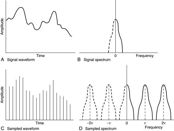
The original frequency spectrum can be easily reconstructed in the example shown in Figure 18. It should, however, be clear that, as the maximum signal frequency, fmax, increases, the individual spectra will widen and begin to overlap. Under these conditions, it becomes impossible to separate the contributions from the individual portions of the spectra, and the original signal cannot then be accurately reproduced. Overlapping occurs when fmax reaches half the sampling frequency. Thus, for accurate reproduction of a continuous signal containing frequencies up to fmax, the sampling rate, v, must be greater than or equal to 2fmax. This condition is known as Nyquist's sampling theorem and applies to sampling at a constant frequency. Obviously, sampling using unequal time intervals complicates the detail of the discussion, but the same general principles apply.
9.3. Aliasing
Figure 18(D) shows that if any component of the signal exceeds ½v, the effect of sampling will be to reproduce those signal components at a lower frequency. This phenomenon, known as aliasing, may be visualized by considering an extreme case where a signal of frequency fsig is sampled at a rate equal to fsig (i.e., v = fsig). Clearly, each sample will be obtained at the same point within each signal cycle and, consequently, the sampled waveform will have a frequency of zero as illustrated in Figure 19(A). Consider next the case where fsig is only very slightly greater than v. Each successive sample will advance by a small amount along the signal cycle as shown in Figure 19(B). The resulting train of samples will appear to vary with a new (lower) frequency, one that did not exist in the original waveform! These so-called alias, or beat, frequencies can cause severe problems in systems which perform any type of signal reconstruction or processing—that is, virtually all DA&C applications.
Figure 19. Generation of alias frequencies.
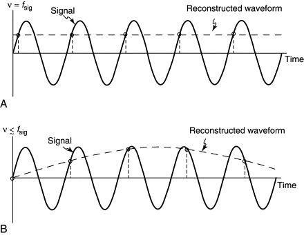
As a digression, it is interesting to note that some systems (although not usually PC-based DA&C systems) exploit the aliasing phenomenon in order to extract information from high-frequency signals. This technique is used in dynamic testing of ADCs and in various types of instrumentation.
In normal sampling applications, however, aliasing is not desirable. It can be avoided by ensuring, first, that the signal is band limited (i.e., has a well-defined maximum frequency, fmax) and, second, that the sampling rate, v, is at least twice fmax. It is usual to employ an analog antialiasing low-pass filter in order to truncate the signal spectrum to the desired value of fmax prior to sampling. This results in the loss of some information from the signal, but by judicious selection of the filter characteristics it is usually possible to ensure that this does not have a significant effect on the performance of the system as a whole. Antialiasing filters are often an integral part of signal-conditioning units. Strain-gauge-bridge signal conditioners, for example, may incorporate filters with a bandwidth of typically 100 to 200 Hz.
It should be borne in mind that no filter possesses an ideal response (i.e., 100%attenuation above the cutoff frequency, f0, and 0% attenuation at lower frequencies), although good antialiasing filters often possess a steep cutoff rate. Because real filters exhibit a gradual drop in response, it is usually necessary to ensure that v is somewhat greater than 2f0. The sampling rate used will depend upon the form of the signal and upon the degree of precision required. The following figures are provided as a rough guide. Simple one- or two-pole passive antialiasing filters may necessitate sampling rates of 5f0 to 10f0. The steeper cutoff rate attainable with active antialiasing filters normally allows sampling at around 3f0.
9.4. Sampling Accuracy
Nyquist' sampling theorem imposes an upper limit on the signal frequencies that can be sampled. However, a number of practical constraints must also be borne in mind. In many applications, the speed of the software (cycling time, interrupt latencies, transfer rate, etc.) restricts the sampling rate and hence fmax. Some systems perform high-speed data capture completely in hardware, thereby circumventing some of the software speed limitations. In these cases, periodic sampling is usually triggered by an external clock signal and the acquired data is channeled directly to a hardware buffer.
The performance of the hardware itself also has a bearing on the maximum frequency that can be sampled with a given degree of accuracy. There is an inherent timing error associated with the sampling and digitization process. This inaccuracy may be a result of the ADC' conversion time or, if a sample-and-hold circuit is employed, it may be caused by the circuit' finite aperture time or aperture jitter. The amount by which the signal might vary in this time limits the accuracy of the sample and is known as the aperture error.
Consider a time-varying measurand, R. For a given timing uncertainty, δt, the accuracy with which the measurand can be sampled will depend upon the maximum rate of change of the signal. To achieve a given measurement accuracy we must place an upper limit on the signal frequency that the system will be able to sample.
We can express a single frequency (f) component as (13)
![]()
The aperture error, A, is defined as (14)
![]() and our sampling requirement is that the aperture error must always be less than some maximum permissible change, δRmax, in R; that is, (15)
and our sampling requirement is that the aperture error must always be less than some maximum permissible change, δRmax, in R; that is, (15) ![]()
We must decide on a suitable value for δRmax. It is usually convenient to employ the criterion: δRmax = 1 LSB (i.e., that A must not exceed 1 LSB). It might be more appropriate in some applications to use different values, however. Applying this criterion and assuming that the full ADC conversion range exactly encompasses the entire signal range (i.e., 2R0), Equation (14) becomes (16)
![]()
Here, n represents the ADC resolution (number of bits). Differentiating Equation (13), we see that the maximum rate of change R is given by 2πfR0. Substituting this into Equation(14), we obtain the maximum frequency, fA, that can be sampled with the desired degree of accuracy: (17)
![]()
Let us consider a moderately fast, 12-bit ADC with a conversion time of 10 μs. Such a device should be able to accommodate sampling rates approaching 100 kHz. Applying the Nyquist criterion gives a maximum signal frequency of half this (i.e., 50 kHz). However, this criterion only guarantees that, given sufficiently accurate measuring equipment, it will be possible to detect this maximum signal frequency. It takes no account of the sampling precision of real ADCs. To assess the effect of finite sampling times we must use Equation (17). Substituting the 10 μs conversion time for δt shows that we would be able to sample signal components up to only 7.7 Hz with the desired 1 LSB accuracy! This illustrates the importance of the greater temporal precision achievable with S/H circuits. If we were to employ an S/H circuit, δt could be reduced to the S/H's aperture jitter time. Substituting a typical value of 2 ns for δt shows that, with the benefit of an S/H circuit, the maximum frequency that could be sampled to a 1 LSB accuracy increases to around 39 kHz.
It is often more useful to calculate the actual aperture error resulting from a particular combination of aperture time and signal frequency. Equation (14) defines the aperture error. This has its maximum value when R is subject to its maximum rate of change. We have already seen that this occurs when R is zero and that the maximum rate of change of R is 2πfR0. The maximum possible aperture error, Amax, is therefore (18)
![]()
Figure 20 depicts values of the ratio Amax/2R0 as a function of aperture time and signal frequency.
Figure 20. Fractional aperture error as a function of aperture time and signal frequency.
9.5. Reconstruction of Sampled Signals
The accuracy with which a signal can be sampled is by no means the only consideration. The ability of the DA&C system to precisely reconstruct the signal (either physically via a DAC or mathematically inside the PC) is often of equal importance. The accuracy with which the sampled signal can be reconstructed depends upon the reconstruction method adopted—that is, upon the physical or mathematical technique used to interpolate between sampled points.
A linear interpolation (known as first-order reconstruction) approximates the signal by a series of straight lines joining each successive sampled data point (see Figure 21). This gives a waveform with the correct fundamental frequency together with many additional higher-frequency components.
Figure 21. Reconstruction of sampled signals: (A) zero-order and (B) first-order interpolation.
Alternatively, we may interpolate by holding the signal at a fixed value between consecutive points. This is known as zero-order reconstruction and is, in effect, the method employed when samples are passed directly to a DAC. In this case, the resulting reconstructed signal will contain a number of harmonics at v ± f, 2v ± f, 3v ± f, and so forth. An electronic low-pass filter would be required at the DAC' output in order to remove the harmonics and thereby smoothly interpolate between samples. Note that these harmonics are artifacts of the reconstruction process, not of the sampling process per se.
The accuracy of the reconstruction will, of course, depend upon the ratio of the signal and sampling frequencies (v/f). There is clearly an error associated with each reconstructed point. Ignoring any errors introduced by the sampling mechanism, the reconstruction error will simply be the difference between the reconstructed value and the actual signal value at any chosen instant. In those parts of Figure 21 where high-frequency signal components predominate (i.e., where the signal is changing most rapidly), there is a potential for a large difference between the original and reconstructed waveforms. The reconstructed waveform will model the original sampled waveform more accurately if there are many samples per signal cycle.
The values of the average and maximum errors associated with the reconstruction are generally of interest to DA&C system designers. It is a trivial matter to derive an analytical equation for the maximum error associated with a zero-order reconstruction, but the calculations necessary to determine the average errors can be somewhat more involved. For this reason we will simply quote an empirical relation. The following formula can be used to estimate the magnitudes of the maximum and the average fractional errors (Er) involved in both zero- and first-order reconstruction. (19)
The coefficients of the equation, p and q, depend upon the order of reconstruction and whether the average or maximum reconstruction error is being calculated. These coefficients are listed in Table 4. Do bear in mind that Equation (19) is not a precise analytical formula. It should only be used as a rough guide for values of v/f greater than about 10.
Table 4. Coefficients of Equation (19)
| Order | Desired calculation | p | q |
|---|---|---|---|
| Zero | Maximum error | 3.1 | −1 |
| Zero | Average error | 2.0 | −1 |
| First | Maximum error | 4.7 | −2 |
| First | Average error | 2.0 | −2 |
Note that the sampling rate required to achieve a desired degree of accuracy with zero-order reconstruction may be several orders of magnitude greater than that necessary with first-order interpolation. For this reason, first-order techniques are to be preferred in general. Appropriate filtering should also be applied to DAC outputs to minimize zero-order reconstruction errors.
In summary, the accuracy of the sampled waveform and the presence of any sampling artifacts will depend upon how the sampled data is processed. Also, the extent to which any such artifacts are acceptable will vary between different applications. All of these points will have a direct bearing on the sampling rate used and must be considered when designing a DA&C system.
9.6. Selecting the Optimum Sampling Rate
In designing a DA&C system, we must assess the effect of ADC resolution, conversion time and S/H aperture jitter, as well as the selected sampling rate on the system's ability to achieve some desired level of precision. For the purposes of the present discussion, we will ignore any inaccuracies in the sensor and signal-conditioning circuits, but we must bear in mind that, in reality, they may affect the accuracy of the system as a whole. We will concentrate here upon sampling rate and its relationship to frequency content and filtering of the signal. In this context, the following list outlines the steps required to ensure that a DA&C system meets specified sampling-precision criteria.
- First, assess the static precision of the ADC (i.e., its linearity, resolution etc.) using Equations (6) and (11) to ensure that it is capable of providing the required degree of precision when digitizing an unchanging signal.
- Assess the effect of sampling rate on the accuracy of signal reconstruction using Equation (19). By this means, determine the minimum practicable sampling rate, v, needed to reproduce the highest-frequency component in the signal with the required degree of accuracy. Also bear in mind Nyquist's sampling theorem and the need to avoid aliasing. From v, you should be able to define upper limits for the ADC conversion time and software cycle times (interrupt rates or loop-repeat rates etc.). Ensure that the combination of software routines and DA&C/computer hardware are actually capable of achieving this sampling rate. Also ensure that appropriate antialiasing filters are employed to remove potentially troublesome high frequencies.
- Given the sample rate, the degree of sampling accuracy required and the ADC resolution, n, use Equations (15) to (17) to define an upper limit on δt and thereby ensure that the digitization and S/H components are capable of providing the necessary degree of sampling precision.
10. Noise and Filtering
Noise can be problematic in analog measuring systems. It may be defined as any unwanted signal component that tends to obscure the information of interest. There are a variety of possible noise sources, such as electronic noise or electromagnetic interference from mains or high-frequency digital circuits. These sources tend to be most troublesome with low-level signals such as those generated by strain gauges and thermocouples. Additionally, noise may also arise from real variations in some physical variable—such as unwanted vibrations in a displacement measuring system or temperature fluctuations due to convection and turbulence in a furnace. As we have seen, the approximations involved in the digitization process are also a source of noise. The presence of noise can be very problematic in some applications. It can make displays appear unsteady, obscure underlying signal trends, erroneously trigger comparators, and seriously disrupt control systems.
It is always good practice to attempt to exclude noise at its source rather than having to remove it at a later stage. Steps can often be taken, particularly with cables and shielding, to minimize noise amplitudes. This topic was discussed briefly and further guidance may be found in the text by Tompkins and Webster (1988) or in various manufacturers' application notes and data books, such as Burr Brown Corp.'s PCI Handbook (1988). However, even in the best-designed systems, a certain degree of noise pickup is often inevitable. If residual noise amplitudes are likely to have a significant effect on the accuracy of the system, the signal-to-noise ratio must be improved before the underlying signal can be adequately processed. This can be accomplished by using simple passive or active analog filter circuits. Filtering can also be performed digitally by using suitable software routines.
Software techniques have a number of advantages over hardware filters. Foremost among these is flexibility. It is very simple to adjust the characteristics of a digital filter by modifying one or two parameters of the filtering algorithm. Another benefit is that digital filters are more stable and do not exhibit any dependence on environmental factors such as temperature. They are also particularly suited to use at very low frequencies, where hardware filters may be impracticable due to their size, weight, or cost. In addition, they are the only way of removing noise introduced by the ADC circuitry during digitization.
Filtering of acquired data can be performed after the data acquisition cycle has been completed. In some ways this approach is the simplest, as the complete data set is available and the filtering algorithm can be easily adjusted to optimize noise suppression. There are many techniques for postacquisition filtering and smoothing of data. Most are based on Fourier methods and are somewhat mathematical. They are classed as data analysis techniques and, as such, fall beyond the scope of this book. Press et al. (1992) describe a number of postacquisition filtering and smoothing techniques in some detail.
Postacquisition filtering is of little use if we need to base real-time decisions or control signals on a filtered, noise-free signal. In this case we must employ real-time filtering algorithms, which are the topic of this section. The design of real-time digital filters can also be quite involved and requires some moderately complex mathematics. However, this section refrains from discussing the mathematical basis of digital filters and, instead, concentrates on the practical implementation of some simple filtering algorithms. While the techniques presented will not be suitable for every eventuality, they will probably cover a majority of DA&C applications. Digital filters can generally be tuned or optimized at the development stage or even by the end user and, for this purpose, a number of empirical guidelines are presented to aid in filter design.
10.1. Designing Simple Digital Filters
It is impossible for DA&C software to determine the relative magnitudes of the signal and noise encapsulated in a single isolated reading. Within one instantaneous sample of the total signal-plus-noise voltage, the contribution due to noise is indistinguishable from that due to the signal. Fortunately, when we have a series of samples, noise and signal can often be distinguished on the basis of their frequencies. They usually have different frequency characteristics, each existing predominantly within well-defined frequency bands. By comparing and combining a series of readings it is possible to ascertain what frequencies are present and then to suppress those frequencies at which there is only noise (i.e., no signal component). The process of removing unwanted frequencies is known as filtering.
10.1.1. Signal and Noise Characteristics
Many signals vary only slowly. We have already seen that some types of sensor and signal-conditioning circuits have appreciable time constants. Noise, on the other hand, may occur at predominantly one frequency (e.g., the mains 50/60 Hz frequency) or, more often, in a broad band as shown in Figure 22. The signal frequencies obtained with most types of sensor will generally be quite low. On the other hand, noise due to radiated electromagnetic pickup or from electronic sources often has a broad spectrum extending to very high frequencies. This high-frequency noise can be attenuated by using an appropriate low-pass filter (i.e., one that suppresses high frequencies while letting low frequencies pass through unaffected). Noise might also exist at low frequencies, overlapping the signal spectrum. Because it occupies the same frequencies as the signal itself, this portion of the noise spectrum cannot be filtered out without also attenuating the signal.
Figure 22. Typical noise and signal spectra.
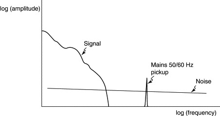
When designing a digital filter, it is advisable to first determine the principal sources of noise in the system and to carefully assess the noise and signal spectra present. Such an exercise provides an essential starting point for determining which frequency bands you wish to suppress and which bands you will need to retain.
10.1.2. Filter Characteristics
Low-pass filters attenuate all frequencies above a certain cutoff frequency, f0, while leaving lower frequencies (virtually) unaffected. Ideally, such filters would have a frequency characteristic similar to curve (a) shown in Figure 23. In practice, this is impossible to achieve, and filter characteristics such as that indicated by curve (b) are more usually obtained with either electronic or digital (software) filters. Other filter characteristics are sometimes useful. High-pass filters, curve (c), for example, suppress frequencies lower than some cutoff frequency while permitting higher frequencies to pass. Bandpass filters, curve (d), allow only those frequencies within a well-defined band to pass, as shown in Figure 23. Although it is possible to construct digital high-pass and bandpass filters, these are rarely needed for real-time filtration and we will, therefore, concentrate on low-pass filters.
Figure 23. Typical filter characteristics.
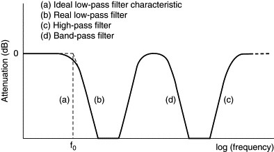
The filter characteristic generally has a rounded shoulder, so the cutoff point is not sharp. The attributes of the filter may be defined by reference to several different points. Sometimes, the frequency at which the signal is attenuated to −3 dB is quoted. In other instances, the curve is characterized by extrapolating the linear, sloping portion of the curve back to the 0-dB level in order to define the cutoff frequency, f0.
In most situations, the noise suppression properties of a filter are only weakly dependent upon f0. Small differences in f0 from some ideal value generally have only a small effect on noise attenuation. This is fortunate as it can sometimes allow a rough approximation to the desired filter characteristic to be used. However, it is always important to carefully assess the dynamic behavior of digital filter designs to ensure that they operate as expected and within specified tolerances. In particular, when applying a digital filter to an acquired data stream, you should be aware of the effect of the filter' bandwidth on the dynamic performance of the system. It is not only frequencies greater than f0 that are affected by low-pass filters. The filter characteristic may also significantly attenuate signals whose frequencies are up to an order of magnitude less than the cutoff frequency. A signal frequency of f0/8, for example, may be attenuated by typically 0.25%.
10.2. Software Considerations
When assessing the performance of a digital filter design, the programmer should bear in mind that whatever formulas and algorithms the filter is based on, the actual coded implementation will be subject to a number of potential errors. The ADC quantization and linearity errors will, of course, ultimately limit the accuracy of the system. However, there is another possible source of error that should be considered: the accuracy of the floating-point arithmetic used.
Some filter algorithms are recursive, using the results of previous calculations in each successive iteration. This provides the potential for floating-point rounding errors to accumulate over time. If rounding errors are significant, the filter may become unstable. This can cause oscillations or an uncontrolled rise in output. It may also prevent the filter's output from decaying to zero when the input signal is removed (i.e., set to zero). Filter routines should normally be implemented using high-precision arithmetic. Using C's double or long double types, rather than the float data type, will usually be sufficient to avoid significant rounding errors.
Although floating-point software libraries can be employed to perform the necessary calculations, a numeric coprocessor will greatly enhance throughput. The speed of the filter routines may be improved by coding them so as to minimize the number of multiplication and division operations required for each iteration. Where you have to divide a variable by a constant value, multiplying by the inverse of the constant instead will generally provide a slight improvement in execution speed.
10.3. Testing Digital Filters
It is essential that you thoroughly check the performance of all filter routines before you use them in your application. This can be accomplished by creating a test routine or program that generates a series of cosinusoidal signals over a range of different frequencies. At each frequency, f, the signal is given by (20)
![]() where t represents elapsed time. In practice, the signal, s, can be determined at each sample time without recourse to real-time calculations by expressing t as the ratio of the ordinal index, k, of each sample to the sampling frequency, v, giving (21)
where t represents elapsed time. In practice, the signal, s, can be determined at each sample time without recourse to real-time calculations by expressing t as the ratio of the ordinal index, k, of each sample to the sampling frequency, v, giving (21)
 So, we can generate the signal for a range of different relative frequencies (f/v). Starting from a maximum value of ½ (the Nyquist limit), the ratio f/v should be gradually reduced until the desired frequency range has been covered.
For each frequency used, s should be evaluated repeatedly in a loop (with k being incremented on each pass through the loop) and each value of s should be passed to the digital filter routine. The filtered cosinusoidal signal can then be reconstructed and its amplitude and phase determined and plotted against f/v. Note that the filter' output will generally be based on a history of samples. Because of this the filter will require a certain number of sampled data points before reaching a steady state. You should, therefore, allow sufficient iterations of the loop before assessing the amplitude and phase of the filtered signal.
10.4. Simple Averaging Techniques
The most obvious way of reducing the effects of random noise is to calculate the average of several readings taken in quick succession. If the noise is truly random and equally distributed about the actual signal level, it should tend to average out to zero. This approach is very simple to implement and can be used in applications with fixed signals (e.g., dimensional gauging of cast steel components) or with very slowly varying signals (e.g., temperature measurements within a furnace). If the signal changes significantly during the sampling period, the averaging process will, of course, also tend blur the signal. The period between samples must be short enough to prevent this but also long enough to allow true averaging of low-frequency noise components.
The main drawback with the simple averaging process—particularly in continuous monitoring or control systems—is that the filter' output is updated at only 1/Nth of the sampling rate (where N is the number of samples over which the average is calculated). If the filtered signal is then used to generate an analog control signal, the delay between successive outputs will increase the magnitude of the reconstruction error.
The simple averaging method is useful in a number of situations. However, if it is necessary to measure changing signals in the presence of noise, a more precise analysis of the filter's frequency characteristics are required and it is usually preferable to employ one of the simple low-pass filtering techniques described in the following section.
10.5. Low-Pass Filtering Techniques
Ideally a software filter routine should be invoked once for each new sample of data. It should return a filtered value each time it is called, so that the filtered output is updated at the sampling frequency.
There are two distinct classes of filter: recursive and nonrecursive. In a no-recursive filter, the output will depend on the current input as well as on previous inputs. The output from recursive filters, on the other hand, is based on previous output values and the current input value. The ways in which the various input and output values are combined varies between different filter implementations, but in general each value is multiplied by some constant weight and the results are then summed to obtain the filtered output.
If we denote the sequence of filter outputs by yk and the inputs (samples) by xk, where k represents the ordinal index of the iteration, a nonrecursive filter is described by the equation (22)
 Here, the constants ai represent the weight allotted to each element in the summation. In general the series of ai values is defined so that the most recent data is allocated the greatest weight. The ai constants often follow an exponential form that allows the filter to model an electronic low-pass filter based on a simple
RC network.
Here, the constants ai represent the weight allotted to each element in the summation. In general the series of ai values is defined so that the most recent data is allocated the greatest weight. The ai constants often follow an exponential form that allows the filter to model an electronic low-pass filter based on a simple
RC network.
The nonrecursive filter described by Equation (22) is termed an infinite impulse response (IIR) filter because the summation takes place over an unbounded history of filter inputs (i.e., xk + xk−1 + · · · + x2 + x1 + x0). In practice, most nonrecursive filter implementations truncate the summation after a finite number of terms, n, and are termed finite impulse response (FIR) filters. In this case, the nonrecursive filter equation becomes (23)
Recursive filters are obtained by adding a recursive (or autoregressive) term to the equation as follows: (24)
The constants bi in the new term represent weights that are applied to the sequence of previous filter outputs. Equation (24) is, in fact, a general form of the filter equation known as an autoregressive moving average (ARMA) filter. As we shall see later, this equation can be simplified to form the basis of an effective low-pass recursive filter.
In addition, the following sections cover two implementations of the nonrecursive type of filter (the unweighted moving average and the exponentially weighted FIFO). Other filters can be constructed from Equations (23) or (24), but for most applications one of the three simple filters described next will usually suffice.
Each weight in Equations (23) and (24) may take either positive or negative values, but the sum of all of the weights must be equal to 1. In a nonrecursive filter, the output signal is effectively multiplied by the sum of the weights and, if this is not unity, the output will be scaled up or down by a fixed factor. The result of using weights that sum to a value greater than 1 in a recursive filter is more problematic. The filter becomes unstable and the output, effectively multiplied by an ever-increasing gain, rises continuously.
Equations (22) to (24) indicate that the time at which each sample, xk, is obtained is not needed in order to calculate the filter output. It is, therefore, unnecessary to pass time data to the filter routines themselves. However, the rate at which the signal is sampled does, of course, have a direct bearing on the performance of the filter. For any given set of filter parameters (i.e., ai, bi, and n), the filter's frequency response curve is determined solely by the sampling rate, v. For example, a filter routine that has a cutoff frequency, f0, of 10 Hz at v = 100 Hz will possess an f0 of 5 Hz if v is reduced to 50 Hz. For this reason we will refer to the filter' frequency characteristics in terms of the frequency ratio, f/v (or f0/v when referring to the cutoff frequency).
10.6. Unweighted Moving Average Filter
The unweighted moving average filter (also sometimes known simply as a moving average filter) is a simple enhancement of the block average technique. It is actually a type of nonrecursive filter based on Equation (23). The weights ai are each set equal to 1/n so that they sum to unity. The filter is described by the following equation: (25)
An FIFO buffer is used to hold the series of x values. The output of the filter is simply the average of all entries held in the FIFO buffer. Because the weights are all equal, this type of filter is also known as an unweighted FIFO filter.
Filters with large FIFO buffers (i.e., large values of n) provide good high-frequency attenuation. They are useful for suppressing noise and unwanted transient signal variations that possess wide-tailed distributions, such as might be present when monitoring the thickness of a rolled sheet product such as rubber or metal sheet.
Listing 2 illustrates how the moving average filter can be implemented. The size of the FIFO buffer is determined by the value defined for N. The InitFilter() function should be called before filtering commences in order to initialize the various FIFO buffer variables. Each subsequent reading (X) should be passed to the Filter() function which will then return the present value of the moving average.
Listing 2. An unweighted moving average filter
- #define N 100 /* Size of FIFO Buffer */
- double FIFO[N];
- int FIFOPtr;
- double FIFOEntries;
- double FIFOTotal;
- void InitFilter()
- f
- FIFOPtr = -1;
- FIFOEntries = 0;
- FIFOTotal = 0;
- }
- double Filter(double X)
- {
- if (FIFOPtr < (N-1))
- FIFOPtr++;
- else FIFOPtr = 0;
- if (FIFOEntries < N)
- {
- FIFOTotal = FIFOTotal + X;
- FIFO[FIFOPtr] = X;
- FIFOEntries = FIFOEntries + 1;
- }
- else {
- FIFOTotal = FIFOTotal - FIFO[FIFOPtr] + X;
- FIFO[FIFOPtr] = X;
- }
- return FIFOTotal / FIFOEntries;
- }
The filter is, of course, least effective during its startup phase when part of the FIFO buffer is still empty. In this phase, the filter's output is calculated by averaging over only those samples that have so far been acquired, as illustrated in the listing. N calls to the Filter() function are required before the FIFO buffer fills with data.
The unweighted moving average filter possesses the frequency characteristic shown in Figure 24. It is clear from the figure that larger FIFO buffers provide better attenuation of high frequencies.
Figure 24. Attenuation vs. frequency relationship for the unweighted moving average filter.
However, because of resonances occurring at even values of v/f and where the FIFO buffer contains an integer number of signal cycles (i.e., when nf/v is an integer), oscillations are present in the characteristic curve at frequencies higher than f0. As a rough rule of thumb, the cutoff frequency is given by v/f0 ∼ 2.5n to 3.0n.
As with all types of filter, a phase lag is introduced between the input and output signals. This tends to increase at higher frequencies. Because of the discrete nature of the sampling process and the resonances just described, the phase vs. frequency relationship also becomes irregular above the cutoff frequency.
This type of filter is very simple but is ideal in applications where high-speed filtration is required. If there is a linear relationship between the measurand and the corresponding digitized reading, the unscaled ADC readings can be processed directly using a moving average filter based on simple integer (rather than floating-point) arithmetic.
10.7. Exponentially Weighted FIFO Filter
The unweighted moving average filter gives equal weight to all entries in the FIFO buffer. Consequently, a particularly large reading will not only affect the filter output when it is supplied as a new input, it will also cause a large change in output when the reading passes through the FIFO buffer and is removed from the summation. To minimize the latter effect, we may apply a decreasing weight to the readings as they pass through the buffer so that less attention is paid to older entries. One such scheme employs an exponentially decreasing series of weights. In this case the weights ai in Equation (23) are given by (26)
![]() Here, t represents the time interval between successive samples (equal to 1/v) and τ is the time constant of the exponential filter-response function. In an ideal filter, with a sufficiently large FIFO
buffer, the series of exponential weights will not be truncated until the weights become insignificantly small. In this case
the time constant, τ, will be related to the desired cutoff frequency by (27)
Here, t represents the time interval between successive samples (equal to 1/v) and τ is the time constant of the exponential filter-response function. In an ideal filter, with a sufficiently large FIFO
buffer, the series of exponential weights will not be truncated until the weights become insignificantly small. In this case
the time constant, τ, will be related to the desired cutoff frequency by (27)
![]() Obviously, in a real filter, the finite size of the FIFO buffer will modify the frequency response, but this effect will
be small provided that nt » τ.
Obviously, in a real filter, the finite size of the FIFO buffer will modify the frequency response, but this effect will
be small provided that nt » τ.
For the purpose of calculating the weights, it is convenient to make use of a constant, r, which represents the number of characteristic exponential time periods (of length τ) that are encompassed by the FIFO buffer: (28)
![]()
The weights are then calculated from (29)
![]()
Substituting Equation (28) into Equation (29) (and remembering that t = 1/v) we see that the expected cutoff frequency of the filter is given by (30)
![]()
This applies only for large values of r (i.e., greater than about 3 in practice) which allow the exponential series of weights to fall from unity—for the most recent sample—to a reasonably low level (typically <0.05) for the oldest sample. Smaller values of r give more weight to older data and result in the finite size of the FIFO buffer becoming the dominant factor affecting the filter' response.
Listing 2 may be easily adapted to include a series of exponential weights as illustrated in Listing 3. The InitFilter() function, which must be called before filtering commences, first calculates a WeightStep value equivalent to the ratio of any two adjacent weights: ai/ai – 1. It also determines the sum of all of the weights. This is required for normalizing the filter output. LowWeight is the weight applied to the oldest entry in the FIFO buffer and is needed in order to calculate the affect of removing the oldest term from the weighted total.
Listing 3. An exponentially weighted FIFO filter
- #define N 100 /* Size of the FIFO buffer */
- #define R 3 /* No. of characteristic time periods within buffer */
- double WeightStep;
- double SumWeights;
- double LowWeight;
- double FIFO[N];
- int FIFOPtr;
- double FIFOEntries;
- double FIFOTotal;
- void InitFilter()
- {
- double T;
- double Weight;
- int I;
- T = R;
- WeightStep = exp(-1 * T / N);
- SumWeights = 0;
- Weight = 1;
- for (I = 0; I < N; I++)
- {
- Weight = Weight * WeightStep;
- SumWeights = SumWeights + Weight;
- }
- LowWeight = Weight;
- FIFOPtr = -1;
- FIFOEntries = 0;
- FIFOTotal = 0;
- }
- double Filter(double S) f
- {
- if (FIFOPtr < (N-1))
- FIFOPtr++;
- else FIFOPtr = 0;
- if (FIFOEntries < N)
- {
- FIFOTotal = (FIFOTotal + S) * WeightStep;
- FIFO[FIFOPtr] = S;
- FIFOEntries = FIFOEntries + 1;
- }
- else {
- FIFOTotal = (FIFOTotal - (FIFO[FIFOPtr] * LowWeight) + S) * WeightStep;
- FIFO[FIFOPtr] = S;
- }
- return FIFOTotal / SumWeights;
- }
The Filter() function should be called for each successive sample. This function records the N most recent samples (i.e., X values) in a FIFO buffer. It also maintains a weighted running total of the FIFO contents in FIFOTotal. The weights applied to each entry in the buffer are effectively reduced by the appropriate amount (by multiplying by WeightStep) as each new sample is added to the buffer.
Good high-frequency attenuation is obtained with r > 1, particularly with the larger FIFO buffers. Phase shifts similar to those described for the moving average filter also occur with the exponentially weighted FIFO filter. Again the effects of resonances and discrete sampling introduce irregularities in the attenuation and phase vs. frequency relationships. As would be expected, this effect is more prominent with values of r less than about 1 to 3. The cutoff frequencies obtained with various combinations of r and n are shown in Figure 25.
Figure 25. Cutoff frequencies vs. r/n for exponentially weighted FIFO filters.
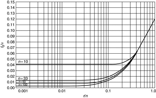
When r is greater than about 3, the f0/v data agrees closely with the expected relationship (Equation [30]). Slight deviations from the ideal response curve are due to the discrete nature of the sampling. Values of r less than about 3 result in a somewhat higher cutoff frequency for a given value of r/n. Conversely, increasing n will reduce f0.
The data in Figure 25 is replotted in Figure 26 which may be used as a basis for choosing values of r and n in practical applications. To determine the values of n and r that are necessary to obtain a given f0:
- Determine v (remembering that it should be high enough to avoid aliasing) and then calculate the desired f0/v.
- Refer to Figure 26 to choose a suitable combination of r and n. The optimum value of r is generally about 3, but values between about 1 and 10 can give adequate results (depending upon n).
- Consider whether the FIFO buffer size (n) indicated is practicable in terms of memory requirements and filter startup time. If necessary use a smaller FIFO buffer (i.e., smaller n) and lower value of r to achieve the desired f0.
Figure 26. Cutoff frequencies vs.n for exponentially weighted FIFO filters.
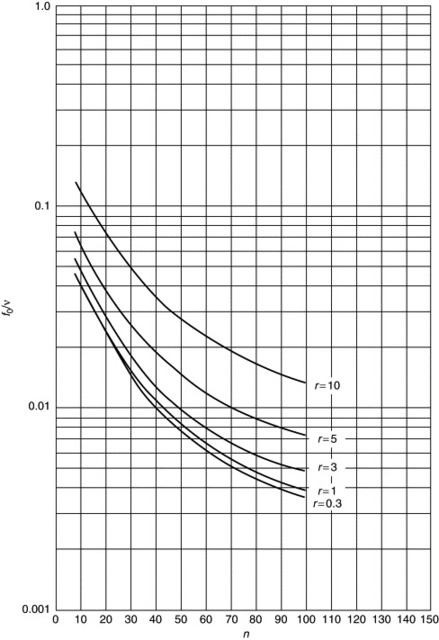
A number of points should be borne in mind when selecting r and n. With small r values, a greater weight is allocated to older data and this lowers the cutoff frequency.
When r < 1 the filter behaves very much like an unweighted moving average filter because all elements of the FIFO buffer have very similar weights. The cutoff frequency is then dependent only on n (i.e., it is only weakly dependent on r) and is determined by the approximate relationship f0/v ∼ (2.5n)−1 to (3n)−1. Only when r is greater than about 2 to 3 is there any strong dependence of f0 on i.
When r is greater than about n/3, the performance of the filter depends only on the ratio r/n because the exponential weights fall to an insignificantly small level, well within the bounds of the FIFO buffer. There is usually no advantage to be gained from operating the filter in this condition as only a small portion of the FIFO buffer will make any significant contribution to the filter's output. If you need to achieve a high f0 it is far better to increase v or, if this is not possible, to reduce n, rather than increasing r beyond n/3. Best results are often obtained with an r value of about 3. This tends to generate a smoothly falling frequency response curve with a well defined f0 and good high-frequency attenuation.
10.8. Recursive Low-Pass Filter
A very effective low-pass filter can be implemented using the general recursive filter Equation (24). The equation may be simplified by using only the most recent sample xk (by setting ai = 0 for i > 0) and the previous filter output yk−1 (by setting bi = 0 for i ≠ 1). The filter equation then reduces to (31)
![]() where (32)
where (32)
![]()
In Equation (31) the 0 and 1 subscripts have been dropped from the weights a and b respectively. As discussed previously, the condition (32) is required for stability. It should be clear that the filter output will respond more readily to changes in x when a is relatively large. Thus the cutoff frequency, f0, will increase with a. Knowing the sampling frequency, v, the constant a can be calculated from the required value of f0 as follows: (33)
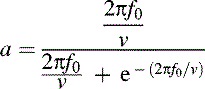 When v » f0, the denominator tends to unity and Equation (33) becomes (34)
![]()
Ideally, the cutoff frequency should be somewhat less than v/20 in order to achieve reasonable attenuation at high frequencies. In this case, the approximation given in Equation (34) introduces only a small error in the cutoff frequency and this generally has a negligible effect on the performance of the filter.
Listing 4 shows how this simple recursive filter can be implemented in practice. The filter coefficient, a, is defined in the listing as the constant A. In this case it is set to 0.1, but other values may be used as required. The InitFilter() function must be called before the sampling sequence starts. It initializes a record of the previous filter output, Y, and calculates the other filter coefficient, b, which is represented by the variable B in the listing. This function may be modified if required to calculate coefficients a and b (i.e., the program variables A and B) from values of f0 and v supplied in the argument list. The Filter() function itself simply calculates a new filter output (using Equation [31]) each time that it is called.
Listing 4. A recursive low-pass filter
- #define A 0.1 /* Modify this value as necessary */
- double Y;
- double B;
- void InitFilter()
- {
- Y = 0;
- B = 1.0 - A;
- }
- double Filter(double X)
- {
- Y = X * A + Y * B;
- return Y;
- }
Figure 27 illustrates the attenuation and phase lag vs. frequency characteristics obtained with a number of different values of a. The relationship between f0 and a follows the form expressed in Equation (34) very closely. For a given value of f0/v, there is little difference between the characteristics of the recursive low-pass filter and the optimum (r = 3) exponentially weighted nonrecursive (FIFO) filter. In general, however, the recursive filter exhibits a smoother falloff of response and there are no resonances at high frequencies. The phase vs. frequency curve is also more regular than that obtained with the exponentially weighted FIFO filter. Note that at the cutoff frequency the phase lag is 45°.
Figure 27. Attenuation and phase characteristics of the recursive low-pass filter.

References
Burr Brown Corporation 1988 Burr Brown Corporation PCI Handbook 1988 Burr Brown Corp Tucson, AZ
Eggebrecht 1990 L.C. Eggebrecht, Interfacing to the IBM Personal Computer 2nd ed 1990 Howard W. Sams Indianapolis
Labfacility Ltd. 1987 Labfacility Ltd Temperature Sensing with Thermocouples and Resistance Thermometers: A Practical Handbook 1987 Labfacility Ltd. Middlesex, UK
Parr 1986 E.A. Parr, Industrial Control Handbook Transducers vol. 1 1986 Collins
Pople 1979 J. Pople, BSSM Strain Measurement Reference Book 1979 British Society of Strain Measurement Newcastle-upon-Tyne, UK
Press 1992 W.H. Press, B.P. Flannery, S.A. Teukolsky, W.T. Vetterling, Numerical Recipes in Pascal: The Art of Scientific Computing 1992 Cambridge University Press Cambridge, UK
Sanchez 1994 J. Sanchez, M.P. Canton, PC Programmer's Handbook 2nd ed 1994 McGraw-Hill New York
Tompkins 1988 W.J. Tompkins, J.G. Webster, Interfacing Sensors to the IBM PC 1988 Prentice-Hall Englewood Cliffs, NJ
Tooley 1995 M.H. Tooley, PC-Based Instrumentation and Control 2nd ed 1995 Butterworth–Heinemann Oxford, UK
van Gilluwe 1994 F. van Gilluwe, The Undocumented PC: A Programmer's Guide to I/O, CPUs, and Fixed Memory Areas 1994 Addison-Wesley Reading, MA
Vears 1990 R.E. Vears, Microprocessor Interfacing 1990 Butterworth–Heinemann Oxford, UK
Warring 1985 R.H. Warring, S. Gibilisio, Fundamentals of Transducers 1985 TAB Books New York