
Chapter 17. Real-World Measurement Applications - Precision Measurement and Sensor Conditioning
17.1. Introduction
The high-resolution Σ-Δ measurement ADC has revolutionized the entire area of precision sensor signal conditioning and data acquisition. Modern Σ-Δ ADCs offer no-missing-code resolutions to 24 bits and greater than 19 bits of noise-free code resolution. The inclusion of on-chip PGAs coupled with the high resolution virtually eliminates the need for signal conditioning circuitry—the precision sensor can interface directly with the ADC in many cases.
The Σ-Δ architecture is highly digitally intensive. It is therefore relatively easy to add programmable features and offer greater flexibility in their applications. Throughput rate, digital filter cutoff frequency, PGA gain, channel selection, chopping, and calibration modes are just a few of the possible features. One of the benefits of the on-chip digital filter is that its notches can be programmed to provide excellent 50-Hz/60-Hz power supply rejection. In addition, since the input to a Σ-Δ ADC is highly oversampled, the requirements on the antialiasing filter are not nearly as stringent as in the case of traditional Nyquist-type ADCs. Excellent common-mode rejection is also a result of the extensive utilization of differential analog and reference inputs. An important benefit of Σ-Δ ADCs is that they are typically designed on CMOS processes and are therefore relatively low cost.
In applying Σ-Δ ADCs, the user must accept the fact that, because of the highly digital nature of the devices and the programmability offered, the digital interfaces tend to be more complex than with traditional ADC architectures such as successive approximation, for example. However, manufacturers' evaluation boards and associated development software along with complete data sheets can considerably ease the overall design process.
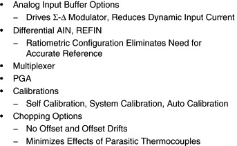
Some of the architectural benefits and features of the Σ-Δ measurement ADC are summarized in Figures 17.1 and 17.2.
Figure 17.1. Σ-Δ ADC architecture benefits.
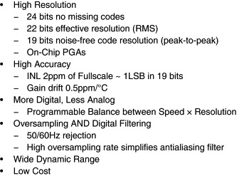
Figure 17.2. Σ-Δ system on-chip features.
17.2. Applications of Precision-Measurement Σ-Δ ADCs
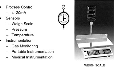
High-resolution measurement Σ-Δ ADCs find applications in many areas, including process control, sensor conditioning, instrumentation, and the like as shown in Figure 17.3. Because of the varied requirements, these ADCs are offered in a variety of configurations and options. For instance, Analog Devices currently (2004) has more than 24 different high-resolution Σ-Δ ADC product offerings available. For this reason, it is impossible to cover all applications and products in a section of reasonable length, so we will focus on several representative sensor conditioning examples which will serve to illustrate most of the important application principles.
Figure 17.3. Typical applications of high-resolution Σ-Δ ADCs.
Because many sensors such as strain gauges, flowmeters, pressure sensors, and load cells use resistor-based circuits, we will use the AD7730 ADC as an example in a weigh scale design. A block diagram of the AD7730 is shown in Figure 17.4.
Figure 17.4. AD7730 single-supply bridge ADC.
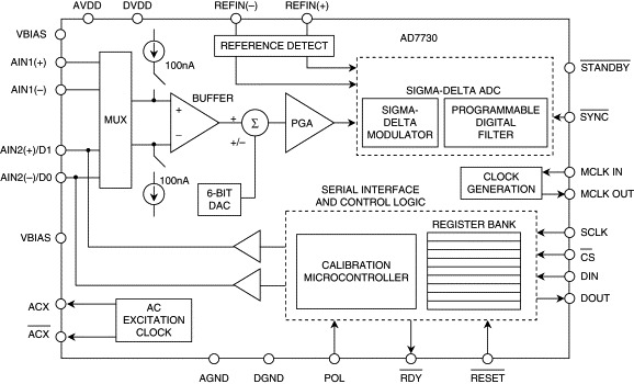
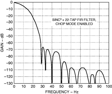
The heart of the AD7730 is the 24-bit Σ-Δ core. The AD7730 is a complete analog front end for weigh scale and pressure measurement applications. The device accepts low-level signals directly from a transducer and outputs a serial digital word. The input signal is applied to a proprietary programmable gain front end based around an analog modulator. The modulator output is processed by a low-pass programmable digital filter, allowing adjustment of filter cutoff, output rate, and settling time. The response of the internal digital filter is shown in Figure 17.5.
Figure 17.5. AD7730 digital filter frequency response.
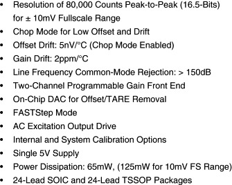
The part features two buffered differential programmable gain analog inputs as well as a differential reference input. The part operates from a single 5-V supply. It accepts four unipolar analog input ranges: 0 mV to +10 mV, +20 mV, +40 mV, and +80 mV and four bipolar ranges: ±10 mV, ±20 mV, ±40 mV, and ±80 mV. The peak-to-peak noise-free code resolution achievable directly from the part is 1 in 230,000 counts. An on-chip 6-bit DAC allows the removal of tare voltages.
Clock signals for synchronizing AC excitation of the bridge are also provided. The serial interface on the part can be configured for three-wire operation and is compatible with microcontrollers and digital signal processors. The AD7730 contains self-calibration and system-calibration options and features an offset drift of less than 5 nV/° C and a gain drift of less than 2 ppm/° C.
The AD7730 is available in a 24-pin plastic DIP, a 24-lead SOIC, and 24-lead TSSOP package. The AD7730L is available in a 24-lead SOIC and 24-lead TSSOP package. Key specifications for the AD7730 are summarized in Figure 17.6. Further details on the operation of the AD7730 can be found in References [1] and [2].
Figure 17.6. AD7730 key specifications.
A very powerful ratiometric technique that includes Kelvin sensing to minimize errors due to wiring resistance and also eliminates the need for an accurate excitation voltage is shown in Figure 17.7. The AD7730 measurement ADC can be driven from a single supply voltage which is also used to excite the remote bridge. Both the analog input and the reference input to the ADC are high impedance and fully differential. By using the + and − SENSE outputs from the bridge as the differential reference to the ADC, the reference voltage is proportional to the excitation voltage which is also proportional to the bridge output voltage. There is no loss in measurement accuracy if the actual bridge excitation voltage varies.
Figure 17.7. AD7730 bridge application showing ratiometric operation and Kelvin sensing.
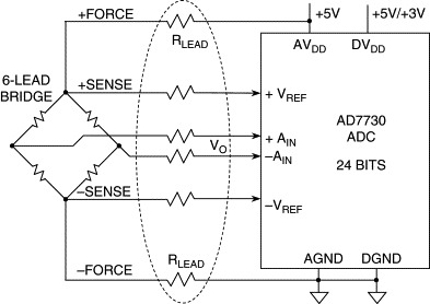
It should be noted that this ratiometric technique can be used in many applications where a sensor output is proportional to its excitation voltage or current, such as a thermistor or RTD.
17.3. Weigh Scale Design Analysis Using the AD7730 ADC
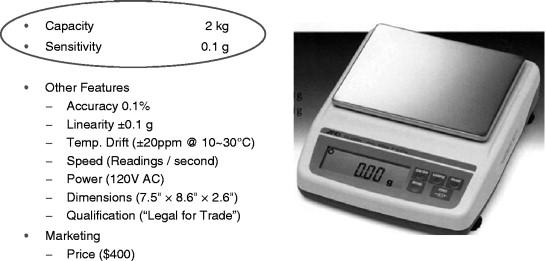
We will now proceed with a simple design analysis of a weigh scale based on the AD7730 ADC and a standard load cell. Figure 17.8 shows the overall design objectives for the weigh scale. The key specifications are the full-scale load (2 kg) and the resolution (0.1 g). These specifications primarily determine the basic load cell and ADC requirements.
Figure 17.8. Design example—weigh scale.
The specifications of a load cell that matches the overall requirements are shown in Figure 17.9. Notice that the load cell is constructed with four individual strain gauges connected in a standard bridge configuration. When the load is applied to the beam, R1 and R2 decrease in value and R3 and R4 increase. This is popularly called the four-element-varying bridge configuration and is described in detail in [1, Chapter 2].
Figure 17.9. Load cell characteristics.
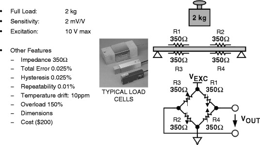
The load cell selected has a full-scale load of 2 kg and an output sensitivity of 2 mV/V. This means that, with an excitation voltage of 10V, the full-scale output voltage is 20 mV. Herein lies the major difficulty in load cell signal conditioning: accurately amplifying and digitizing the low-level output signal without corrupting it with noise. The load cell output is analyzed further in Figure 17.10. With the chosen excitation voltage of 5V, the full-scale bridge output voltage is only 10 mV. Notice that the output is also proportional to (or ratiometric with) the excitation voltage.
Figure 17.10. Determining full-scale output of load cell with 5-V excitation.

The next step is to determine the resolution requirements of the ADC, and the details are summarized in Figure 17.11. The total number of individual quantization levels (counts) required is equal to the full-scale weight (2 kg) divided by the desired resolution (0.1 g), or 20,000 counts. With a 5-V excitation voltage, the full-scale load cell output voltage is 10 mV for a 2-kg load.
Figure 17.11. Determining resolution requirements.
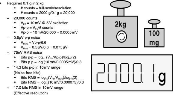
The required noise-free resolution, Vp-p, is therefore given by Vp-p = 10 mV/20,000 = 0.5 μV. This defines the code width, and therefore the peak-to-peak (p-p) noise must be less than 0.5 μV. The corresponding allowable rms noise is given by VRMS = Vp-p/6.6 = 0.5 μV/6.6 = 0.075 μV rms = 75 nV rms. (The factor 6.6 is used to convert peak-to-peak noise to rms noise, assuming gaussian noise).
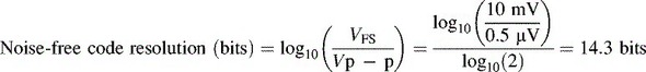
The noise-free code resolution of the ADC is calculated as follows: (17.1)
The effective resolution of the ADC is calculated as follows: (17.2)
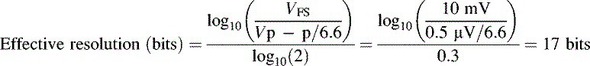
Figure 17.12 shows the traditional sensor conditioning solution to this problem, where an instrumentation amplifier is used to amplify the 10-mV full-scale bridge output signal to 2.5V, which is compatible with the input of the 14+-bit ADC. This approach requires a low-noise, low-drift in amp such as the AD620 precision in-amp [4] which has a 0.1-Hz to 10-Hz peak-to-peak noise of 280 nV, approximately 280 nV ÷ 6.6 = 42 nV rms.
Figure 17.12. Traditional approach to design.
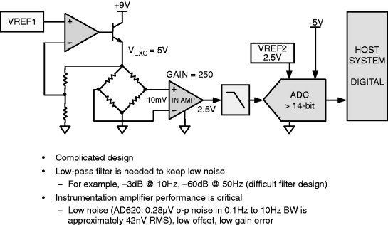
Another critical requirement of the system is a low-pass filter to remove noise and 50-Hz/60-Hz pickup. Assuming a signal 3-dB bandwidth of 10 Hz, the filter should be down at least 60 dB at 50 Hz—a challenging filter design to put it mildly. There are many other considerations in the design including the stability of the two reference voltages, the VREF1 buffer op-amp, and so forth.
Finally, the ADC presents another serious challenge, requiring 14.3-bit noise-free code performance with a 2.5-V full-scale input signal—implying a 16-bit ADC with no more than approximately three LSBs peak-to-peak (0.45 LSBs rms) input-referred noise.
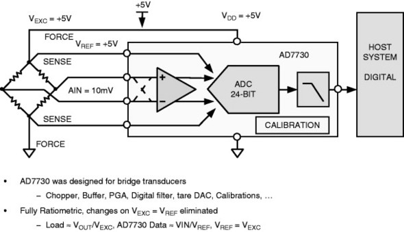
In order to avoid these traditional signal conditioning design problems, the AD7730-based design shown in Figure 17.13 represents a truly elegant solution requiring no instrumentation amplifier, reference, or filter. Note that the bridge interfaces directly with the AD7730 as previously shown in Figure 17.7. The AD7730 input PGA eliminates the need for an external in-amp, providing a full-scale input range of 10 mV as a programmable option. Kelvin sensing is used to eliminate errors due to the wiring resistance in the bridge excitation lines. The bridge is driven directly from the 5-V supply, and the sense lines serve as the ADC reference voltage—thereby ensuring fully ratiometric operation as previously described. The need for a complicated filter is also eliminated—simple ceramic capacitor decoupling on each analog and reference input (not shown on the diagram) is sufficient.
Figure 17.13. Design using AD7730.
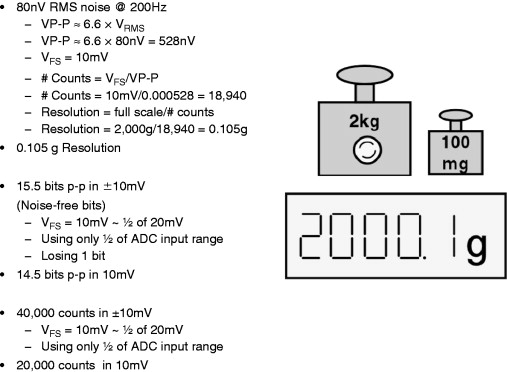
System performance of the design can be determined by a detailed examination of the AD7730 data sheet, Tables I and II, as shown in Figure 17.14. Table I shows the output rms noise in nanovolts as a function of output data rate, digital filter 3-dB frequency, and input range (chopping-mode enabled in all cases). An output data rate of 200 Hz yields a filter corner frequency of 7.9 Hz which is reasonable for the application at hand. With an input range of ±10 mV, the output rms noise is 80 nV. This corresponds to a peak-to-peak noise, Vp-p = 80 nV × 6.6 = 528 nV. The number of noise-free counts is obtained as VFS/Vp-p = 10 mV/528 nV = 18,940. The system resolution for a 2-kg load is therefore 2 kg/18,940 = 0.105 g, which is approximately the required specification of 0.1 g.
Figure 17.14. AD7730 resolution determination from data sheet.
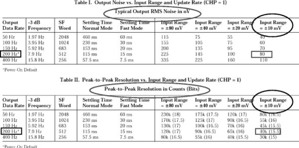
Table II can be also used to determine the noise-free code resolution which is 40,000 counts (15.5 noise-free bits) for a ±10-mV input range. This must be divided by a factor of 2 because only one half the input range is used. Therefore, the actual design will provide approximately 20,000 counts (14.5 noise-free bits), which agrees closely with the previous calculation. The various calculations are summarized in Figure 17.15.
Figure 17.15. AD7730 resolution at 200-Hz data rate.
Note that overall resolution can be increased by dropping back to lower output data rates with correspondingly lower digital filter corner frequencies.
Evaluation of the design is simplified with the AD7730 evaluation board and software as shown in Figure 17.16. The evaluation board can be connected directly to the load cell and the PC. The software allows the various AD7730 options to be varied to evaluate different combinations of data rates, filter frequencies, input ranges, chopping options, and the like. Other ADCs in the AD77xx family have similar evaluation boards and software.
Figure 17.16. Evaluation of design using evaluation board and software.

A summary of the final weigh scale design and specifications is shown in Figure 17.17.
Figure 17.17. Final system performance.

17.4. Thermocouple Conditioning Using the AD7793 ADC
Thermocouples provide accurate temperature measurements over an extremely wide range; however, their relatively small output voltage makes the signal conditioning circuit design difficult. For instance, a Type-K thermocouple has a nominal temperature coefficient of 39 μV/° C, so a temperature change of 1000° C produces only a 39-mV output voltage. The thermocouple does not measure temperature directly—its output voltage is proportional to the temperature difference between the actual measuring junction and the “cold” junction where the thermocouple wires are connected to the measuring electronics. (Details of thermocouple operation are described in [1]).
Accurate thermocouple measurements therefore require that the temperature of the “cold” junction be measured in some manner to compensate for changes in ambient temperature.
The AD7793 dual channel 24-bit Σ-Δ is ideally suited for direct thermocouple measurements, and a simplified block diagram is shown in Figure 17.18 [5].
Figure 17.18. AD7793 24-bit Σ-Δ ADC.
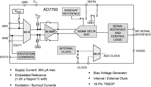
The AD7793 has two differential inputs, an on-chip in-amp, reference voltage, bias voltage generator, and burnout/excitation current sources. Single-supply (5-V) power supply current is 350 μA maximum.
A complete solution to a thermocouple measurement design is shown in Figure 17.19. Notice that a thermistor is used to measure the temperature of the “cold” junction via AIN2, and the thermocouple is connected directly to the AIN1 differential input. Note that the internal VBIAS voltage is used to establish the thermocouple common-mode voltage. The R/C filters minimize noise pickup from the remote thermocouple leads, and typical values of 100Ω and 0.1 μF are reasonable choices.
Figure 17.19. Thermocouple design with cold junction compensation using the AD7793.
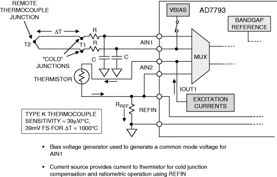
The AD7793 is first programmed to measure the AIN1 thermocouple voltage using the internal 1.2-V bandgap voltage as a reference. This value is sent to a microcontroller connected to the serial interface. The voltage across the thermistor is established by the IOUT1 excitation current which also flows through a reference resistor, RREF. The voltage developed across RREF drives the auxillary reference input, REFIN. The AD7793 is programmed to use the REFIN reference when measuring the thermistor voltage at AIN2. The thermistor voltage is then sent to the microcontroller which performs the required calculations, including the correction for the temperature of the cold junction, T2. The thermistor is therefore connected in a ratiometric fashion such that variations in IOUT1 do not affect the accuracy of the thermistor measurement. Note that the powerful ratiometric technique will work with any resistive-based sensor including thermistors, bridges, strain gauges, and RTDs.
17.5. Direct Digital Temperature Measurements
Temperature sensors with digital outputs have a number of advantages over those with analog outputs, especially in remote applications. Opto-isolators can also be used to provide galvanic isolation between the remote sensor and the measurement system. Although a voltage-to-frequency converter driven by a voltage output temperature sensor accomplishes this function, more sophisticated and more efficient ICs are now available that offer several performance advantages.
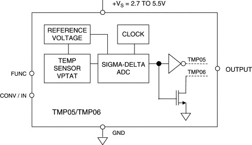
The TMP05/TMP06 digital output sensor family includes a voltage reference, VPTAT generator, Σ-Δ ADC, and a clock source (see Figure 17.20). The sensor output is digitized by a first-order Σ-Δ modulator. This converter utilizes time-domain oversampling and a high-accuracy comparator to deliver 12 bits of effective accuracy in an extremely compact circuit.
Figure 17.20. Digital output temperature sensors: TMP05/06.
The output of the Σ-Δ modulator is encoded using a proprietary technique that results in a serial digital output signal with a mark-space ratio format (see Figure 17.21) which is easily decoded by any microprocessor into either degrees centigrade or degrees Fahrenheit and readily transmitted over a single wire. Most important, this encoding method avoids major error sources common to other modulation techniques, as it is clock independent.
Figure 17.21. TMP05/TMP06 output format.

The TMP05/TMP06 output is a stream of digital pulses, and the temperature information is contained in the mark/space ratio per the equations shown in Figure 17.21. The TMP05/TMP06 has three modes of operation. These are continuously converting, daisy chain, and one shot. A three-state FUNC input selects one of the three possible modes. In the one-shot mode, the power consumption is reduced to 70 μW at one sample per second.
The CONV/IN input is used to determine the rate with which the TMP05/TMP06 measures temperature in the continuously converting and one-shot modes. In the daisy-chain mode, the CONV/IN pin operates as the input to the daisy chain. The daisy-chain mode allows multiple TMP05/TMP06s to be connected together and thus allows one input line of the microcontroller to be the sole receiver of all temperature measurements (see [6] for further details).
Popular microcontrollers, such as the 80C51 and 68HC11, have on-chip timers that can easily decode the mark/space ratio of the TMP05/TMP06. A typical interface to the 80C51 is shown in Figure 17.22. Two timers, labeled Timer 0 and Timer 1, are 16 bits in length. The 80C51's system clock, divided by 12, provides the source for the timers. The system clock is normally derived from a crystal oscillator, so timing measurements are quite accurate. Since the sensor's output is ratiometric, the actual clock frequency is not important. This feature is important because the microcontroller's clock frequency is often defined by some external timing constraint, such as the serial baud rate.
Figure 17.22. Interfacing TMP06 to a microcontroller.

Software for the sensor interface is straightforward. The microcontroller simply monitors I/O port P1.0, and starts Timer 0 on the rising edge of the sensor output. The microcontroller continues to monitor P1.0, stopping Timer 0 and starting Timer 1 when the sensor output goes low. When the output returns high, the sensor's T1 and T2 times are contained in registers Timer 0 and Timer 1, respectively. Further software routines can then apply the conversion factor shown in the previous equations and calculate the temperature.
The TMP05/TMP06 are ideal for monitoring the thermal environment within electronic equipment. For example, the surface-mounted package will accurately reflect the thermal conditions that affect nearby integrated circuits.
The TMP05 and TMP06 measure and convert the temperature at the surface of their own semiconductor chip. When they are used to measure the temperature of a nearby heat source, the thermal impedance between the heat source and the sensor must be considered. Often, a thermocouple or other temperature sensor is used to measure the temperature of the source, while the TMP05/TMP06 temperature is monitored by measuring the T1 and T2 pulse widths with a microcontroller. Once the thermal impedance is determined, the temperature of the heat source can be inferred from the TMP05/TMP06 output.
Carrying the integration a step further, we will now look at true temperature-to-digital converters. The basic bandgap reference has been a building block for ADCs and DACs for many years, and most converters have them integrated on-chip. Inside the bandgap reference circuit, there is invariably a voltage or current that is proportional to absolute temperature (PTAT). There is no fundamental reason why this voltage or current cannot be used to sense the temperature of the IC substrate within the ADC. There is also no fundamental reason why the ADC cannot convert this voltage into a digital output word that represents the chip temperature. In the early days of IC data converters, internal power dissipation was considerable, so an internal temperature sensor would measure a temperature greater than the ambient temperature. Modern low-voltage, low-power ICs make it quite practical to use such a concept to produce a true temperature-to-digital converter that accurately reflects the ambient or PC board temperature.
This concept has expanded to an entire family of temperature-to-digital converters as well as ADCs with multiplexed inputs, where one input is the on-chip temperature sensor. This is a powerful feature, since modern microprocessor, DSP, and FPGA chips tend to dissipate lots of power, and most require a certain amount of airflow. A simple means of monitoring the PC board temperature is valuable in protecting these critical circuits against damage from excessive temperatures due to fault conditions.
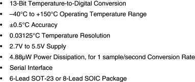
The ADT7301 is a 13-bit digital temperature sensor with a 14th bit as a sign bit [7]. The part contains an on-chip bandgap reference, temperature sensor, a 13-bit ADC, and serial interface logic functions in SOT-23 and MSOP packages. The ADC section consists of a conventional successive-approximation converter based on a switched-capacitor DAC architecture. The parts are capable of running on a 2.7-V to 5.5-V power supply. The on-chip temperature sensor allows an accurate measurement of the ambient device temperature to be made. The specified measurement range of the ADT7301 is −40° C to +150° C. It is not recommended to operate the device at temperatures above 125° C for greater than a total of 5% of the projected lifetime of the device. Any exposure beyond this limit will affect device reliability. A simplified block diagram of the ADT7301 is given in Figure 17.23, and key specifications are summarized in Figure 17.24.
Figure 17.23. ADT7301 13-bit, ±0.5° C accurate, micropower digital temperature sensor.
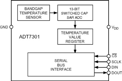
Figure 17.24. ADT7301 key specifications.
The ADT7301 can be used for surface- or air-temperature sensing applications. If the device is cemented to a surface with thermally conductive adhesive, the die temperature will be within about 0.1° C of the surface temperature, thanks to the device's low power consumption. Care should be taken to insulate the back and leads of the device from airflow, if the ambient air temperature is different from the surface temperature being measured. The ground pin provides the best thermal path to the die, so the temperature of the die will be close to that of the printed-circuit ground track. Care should be taken to ensure that this is in good thermal contact with the surface being measured.
As with any IC, the ADT7301 and its associated wiring and circuits must be kept free from moisture to prevent leakage and corrosion, particularly in cold conditions where condensation is more likely to occur. Water-resistant varnishes and conformal coatings can be used for protection. The small size of the ADT7301 package allows it to be mounted inside sealed metal probes, which provide a safe environment for the device.
17.6. Microprocessor Substrate Temperature Sensors
Today's computers require that hardware as well as software operate properly, in spite of the many things that can cause a system crash or lockup. The purpose of hardware monitoring is to monitor the critical items in a computing system and take corrective action should problems occur.
Microprocessor supply voltage and temperature are two critical parameters. If the supply voltage drops below a specified minimum level, further operations should be halted until the voltage returns to acceptable levels. In some cases, it is desirable to reset the microprocessor under “brownout” conditions. It is also common practice to reset the microprocessor on power-up or power-down. Switching to a battery backup may be required if the supply voltage is low.
Under low-voltage conditions it is mandatory to inhibit the microprocessor from writing to external CMOS memory by inhibiting the chip enable signal to the external memory.
Many microprocessors can be programmed to periodically output a “watchdog” signal. Monitoring this signal gives an indication that the processor and its software are functioning properly and that the processor is not stuck in an endless loop.
The need for hardware monitoring has resulted in a number of ICs, traditionally called microprocessor supervisory products, that perform some or all of these functions. These devices range from simple manual reset generators (with debouncing) to complete microcontroller-based monitoring subsystems with on-chip temperature sensors and ADCs. Analog Devices' ADM-family of products is specifically designed to perform the various microprocessor supervisory functions required in different systems.
CPU temperature is critically important in the Pentium® microprocessors. For this reason, all new Pentium devices have an on-chip substrate PNP transistor that is designed to monitor the actual chip temperature. The collector of the substrate PNP is connected to the substrate, and the base and emitter are brought out on two separate pins of the Pentium.
The ADM1023 microprocessor temperature monitor is specifically designed to process these outputs and convert the voltage into a digital word representing the chip temperature. It is optimized for use with the Pentium III microprocessor. The simplified analog signal processing portion of the ADM1023 is shown in Figure 17.25.
Figure 17.25. ADM1023 microprocessor temperature monitor input conditioning circuits.
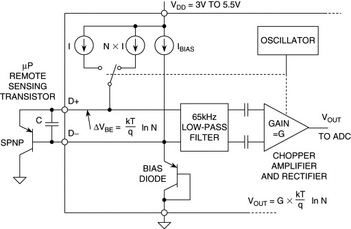
The technique used to measure the temperature is identical to the “ΔVBE” principle. Two different currents (I and N · I) are applied to the sensing transistor, and the voltage measured for each. The change in the base-emitter voltage, ΔVBE, is a PTAT voltage and given by the equation (17.3)
Figure 17.25 shows the external sensor as a substrate PNP transistor, provided for temperature monitoring in the microprocessor, but it could equally well be a discrete transistor such as a 2N3904 or 2N3906. If a discrete transistor is used, the collector should be connected to the base and not grounded. To prevent ground noise interfering with the measurement, the more negative terminal of the sensor is not referenced to ground but is biased above ground by an internal diode. If the sensor is operating in a noisy environment, C may be optionally added as a noise filter. Its value is typically 2200 pF, but should be no more than 3000 pF.
To measure ΔVBE, the sensing transistor is switched between operating currents of I and N · I. The resulting waveform is passed through a 65-kHz low-pass filter to remove noise, then to a chopper-stabilized amplifier which performs the function of amplification and synchronous rectification. The resulting DC voltage is proportional to ΔVBE and is digitized by the ADC and stored as an 11-bit word. To further reduce the effects of noise, digital filtering is performed by averaging the results of 16 measurement cycles.
In addition, the ADM1023 contains an on-chip temperature sensor, and its signal conditioning and measurement is performed in the same manner.
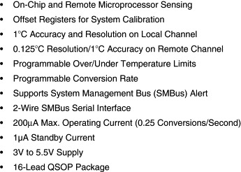
One LSB of the ADM1023 corresponds to 0.125° C, and the ADC can theoretically measure from 0° C to 127.875° C. The results
of the local and remote temperature measurements are stored in the local and remote temperature value registers and are compared
with limits programmed into the local and remote high- and low-limit registers as shown in Figure 17.26. An
![]() output signals when the on-chip or remote temperature is out of range. This output can be used as an interrupt, or as an SMBus
alert.
output signals when the on-chip or remote temperature is out of range. This output can be used as an interrupt, or as an SMBus
alert.
Figure 17.26. ADM1023 simplified block diagram.
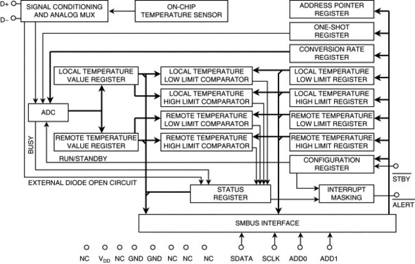
The limit registers can be programmed, and the device controlled and configured, via the serial system management bus (SMBus).
The contents of any register can also be read back by the SMBus. Control and configuration functions consist of switching
the device between normal operation and standby mode, masking or enabling the
![]() output, and selecting the conversion rate which can be set from 0.0625 Hz to 8 Hz. Key specifications for the ADM1023 are
given in Figure 17.27.
output, and selecting the conversion rate which can be set from 0.0625 Hz to 8 Hz. Key specifications for the ADM1023 are
given in Figure 17.27.
Figure 17.27. ADM1023 key specifications.
17.7. Applications of ADCs in Power Meters
While electromechanical energy meters have been popular for over 50 years, a solid-state energy meter delivers far more accuracy and flexibility. Just as important, a well-designed solid-state meter will have a longer useful life. The ADE775x energy-metering ICs are a family products designed to implement this type of meter [9–11].
We must first consider the fundamentals of power measurement (Figure 17.28). Instantaneous AC voltage is given by the expression v(t) = V × cos(ωt), and the current (assuming it is in phase with the voltage) by i(t) = I × cos(ωt). The instantaneous power is the product of v(t) and i(t): (17.4)
![]()
Figure 17.28. Basics of power measurements.
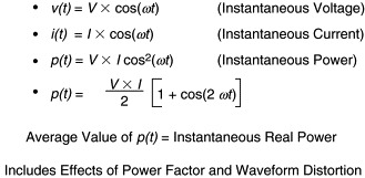
Using the trigonometric identity, (17.5)
![]() (17.6)
(17.6)
![]()
The instantaneous real power is simply the average value of p(t). It can be shown that computing the instantaneous real power in this manner gives accurate results even if the current is not in phase with the voltage (i.e., the power factor is not unity; by definition, the power factor is equal to cos θ, where θ is the phase angle between the voltage and the current). It also gives the correct real power if the waveforms are nonsinusoidal.
The ADE7755 implements these calculations, and a block diagram is shown in Figure 17.29. The two ADCs digitize the voltage signals from the current and voltage transducers. These ADCs are 16-bit second-order Σ-Δ with an input sampling rate of 900 kSPS. This analog input structure greatly simplifies transducer interfacing by providing a wide dynamic range for direct connection to the transducer and also by simplifying the antialiasing filter design. A programmable gain stage in the current channel further facilitates easy transducer interfacing. A high-pass filter in the current channel removes any DC component from the current signal. This eliminates any inaccuracies in the real power calculation due to offsets in the voltage or current signals.
Figure 17.29. ADE7755 energy-metering IC signal processing.

The real power calculation is derived from the instantaneous power signal. The instantaneous power signal is generated by a direct multiplication of the current and voltage signals. In order to extract the real power component (i.e., the DC component), the instantaneous power signal is low-pass filtered. Figure 17.29 illustrates the instantaneous real power signal and shows how the real power information can be extracted by low-pass filtering the instantaneous power signal. This method correctly calculates real power for nonsinusoidal current and voltage waveforms at all power factors. All signal processing is carried out in the digital domain for superior stability over temperature and time.
The low-frequency output of the ADE7755 is generated by accumulating this real power information (see Figure 17.30). This low frequency inherently means a long accumulation time between output pulses. The output frequency is therefore proportional to the average real power. This average real power information can, in turn, be accumulated (e.g., by a counter) to generate real energy information. Because of its high output frequency and shorter integration time, the CF output is proportional to the instantaneous real power. This is useful for system calibration purposes that would take place under steady load conditions.
Figure 17.30. ADE7755 energy-metering IC with pulse output.

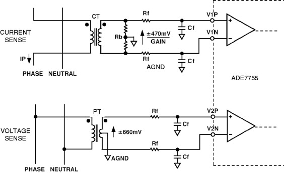
Figure 17.31 shows a typical connection diagram for Channel V1 and V2. A CT (current transformer) is the transducer selected for sensing the Channel V1 current. Notice the common-mode voltage for Channel 1 is AGND and is derived by center tapping the burden resistor to AGND. This provides the complementary analog input signals for V1P and V1N. The CT turns ratio and burden resistor Rb are selected to give a peak differential voltage of ±470 mV/gain at maximum load. The Channel 2 voltage sensing is accomplished with a PT (potential transformer) to provide complete isolation from the power line.
Figure 17.31. Typical connections for Channel 1 (current sense) and Channel 2 (voltage sense).
References
1 Walt Kester, Practical Design Techniques for Sensor Signal Conditioning 1999 Analog Devices Chapter 23, available at www.analog.com
2 Data sheet for AD7730/AD7730L Bridge Transducer ADC, available at www.analog.com.
3 Walter G Jung, Op Amp Applications 2002 Analog Devices Chapter 4
4 Data sheet for AD620 Precision Instrumentation Amplifier, available at www.analog.com.
5 Data sheet for AD7793 24-bit Dual Sigma-Delta ADC, available at www.analog.com.
6 Data sheet for TMP05/TMP06 ±0.5° C Accurate PWM Temperature Sensor in 5-Lead SC-70, available at www.analog.com.
7 Data sheet for ADT7301 13-bit, ±0.5° C Accurate, MicroPower Digital Temperature Sensor, available at www.analog.com.
8 Data sheet for ADM1023 ACPI Compliant High Accuracy Microprocessor System Temperature Monitor, available at www.analog.com.
9 Data sheet for ADE7755 Energy Metering IC with Pulse Output, available at www.analog.com.
10 Paul Daigle, All-Electronic Power and Energy Meters Analog Dialogue 33 no. 2 1999 (February), available at www.analog.com
11 John Markow, Microcontroller-Based Energy Metering Using the AD7755 Analog Dialogue 33 no. 9 1999 (October), available at www.analog.com