
Chapter 9. Interrupt Control and System Control
Overview of the NVIC and System Control Block Features
The Nested Vectored Interrupt Controller (NVIC) is an integrated part of the Cortex-M0 processor. It is closely linked to the processor core logic and provides the functions of interrupt control and system exception support.
Apart from the NVIC, there is also a System Control Block (SCB), which shares the same System Control Space (SCS) memory address range. The SCB contains features for operating system support, like an internal timer for the SysTick exception. The OS-related features will be covered in Chapter 10.
The NVIC features were explored in Chapter 3. Those features include the following:
• Flexible interrupt management include enable/disable, priority configurations
• Hardware nested interrupt support
• Vectored exception entry
• Interrupt masking
The NVIC in the Cortex-M0 processor supports up to 32 external interrupts and one nonmaskable interrupt (NMI). The interrupt input requests can be level triggered, or they can be pulsed with a minimum of one clock cycle. Each external interrupt can be enabled or disabled independently, and its pending status can also be set or clear manually.
The NVIC control registers are memory mapped and can be easily accessed in C language. The location of the NVIC registers starts from address 0xE000E100. For the Cortex-M0 processor, the accesses to the NVIC register must be in word size. (Note that in the Cortex-M3 processor, access to the NVIC can be in the form of word, half-word, or byte transfers.)
Similar to the NVIC registers, the SCB registers are also word accessible, and the address starts from 0xE000E010. The SCB registers handle features like the SysTick timer operations, system exception management and priority control, and sleep mode control.
Interrupt Enable and Clear Enable
The Interrupt Enable control register is a programmable register that is used to control the enable/disable of the interrupt requests (exception 16 and above). The width of this register depends on how many interrupts are supported; the maximum size is 32 bit and the minimum size is 1 bit. This register is programmed via two separate addresses. To enable an interrupt, the SETENA address is used, and to disable an interrupt, the CLRENA address is used (Table 9.1).
Separating the set and clear operations in two different addresses has various advantages. First, it reduces the steps needed for enabling an interrupt, thus getting small code and shorter execution time. For example, to enable interrupt #2, we only need to program the NVIC with one access:
∗((volatile unsigned long ∗)(0xE000E100))=0x4;//Enable interrupt #2
LDRR0,=0xE000E100 ;Setup address in R0
MOVSR1,#0x4;interrupt #2
STRR1,[R0];write to set interrupt enable
The second advantage is that this arrangement prevents race conditions between multiple application processes that can result in the loss of programmed control information. For example, if the enable control is implemented using a simple read/write register, a read-modify-write process is required for enabling an interrupt (e.g., interrupt #2 in this case), and if between the read operation and write operation, an interrupt occurred and the ISR changed another bit in the interrupt-enabled register, the change done by the ISR could be overwritten when the interrupted program resumed.
An interrupt enable can be cleared with the use of similar code, only the address is different. For example, to disable interrupt #2, we use the following code:
LDRR0,=0xE000E180;Setup address in R0
MOVSR1,#0x4;interrupt #2
STRR1,[R0];write to clear interrupt enable
In normal application development, it is best to use the NVIC control functions provided in the CMSIS-compliant device driver library to enable or disable interrupts. This gives your application code the best software portability. CMSIS is part of the device driver library from your microcontroller vendor and is covered in Chapter 4. To enable or disable interrupt using CMSIS, the functions provided are as follows:
void NVIC_EnableIRQ(IRQn_Type IRQn); // Enable Interrupt –// IRQn value of 0 refer to Interrupt #0
void NVIC_DisableIRQ(IRQn_Type IRQn); // Disable Interrupt –// IRQn value of 0 refer to Interrupt #0
Interrupt Pending and Clear Pending
If an interrupt takes place but cannot be processed immediately—for example, if the processor is serving a higher-priority interrupt—the interrupt request will be pended. The pending status is held in a register and will remain valid until the current priority of the processor is lowered so that the pending request is accepted or until the application clears the pending status manually.
The interrupt pending status can be accessed or modified, through the Interrupt Set Pending (SETPEND) and Interrupt Clear Pending (CLRPEND) register addresses (Table 9.2). Similar to the Interrupt Enable control register, the Interrupt Pending status register is physically one register, but it uses two addresses to handle the set and clear the bits. This allows each bit to be modified independently, without the risk of losing information because of race conditions between two application processes.
The Interrupt Pending status register allows an interrupt to be triggered by software. If the interrupt is already enabled, no higher-priority exception handler is running, and no interrupt masking is set, then the interrupt service routine will be carried out almost immediately. For example, if we want to trigger interrupt #2, we can use the following code:
∗((volatile unsigned long ∗)(0xE000E100))=0x4; //Enable interrupt #2
∗((volatile unsigned long ∗)(0xE000E200))=0x4; //Pend interrupt #2
LDRR0,=0xE000E100 ; Setup address in R0
MOVSR1,#0x4; interrupt #2
STRR1,[R0]; write to set interrupt enable
LDRR0,=0xE000E200 ; Setup address in R0
STRR1,[R0]; write to set pending status
In some cases we might need to clear the pending status of an interrupt. For example, when an interrupt-generating peripheral is being reprogrammed, we can disable the interrupt for this peripheral, reprogram its control registers, and clear the interrupt pending status before re-enabling the peripheral (in case unwanted interrupt requests might be generated during reprogramming). For example, to clear the pending status of interrupt 2, we can use the following code:
∗((volatile unsigned long ∗)(0xE000E280))=0x4;// Clear interrupt #2
// pending status
LDRR0,=0xE000E280 ; Setup address in R0
MOVSR1,#0x4; interrupt #2
STRR1,[R0]; write to clear pending status
In the CMSIS-compliant device driver libraries, three functions are provided for accessing the pending status registers:
void NVIC_SetPendingIRQ(IRQn_Type IRQn); // Set pending status of a interrupt
void NVIC_ClearPendingIRQ(IRQn_Type IRQn); // Clear pending status of a interrupt
uint32_t NVIC_GetPendingIRQ(IRQn_Type IRQn); // Return true if the interrupt pending status is 1
Interrupt Priority Level
Each external interrupt has an associated priority-level register. Each of them is 2 bits wide, occupying the two MSBs of the Interrupt Priority Level Registers. Each Interrupt Priority Level Register occupies 1 byte (8 bits). NVIC registers in the Cortex-M0 processor can only be accessed using word-size transfers, so for each access, four Interrupt Priority Level Registers are accessed at the same time (Figure 9.1).

The unimplemented bits are read as zero. Write values to those unimplemented bits are ignored, and read values of the unimplemented bits return zeros (Table 9.3).
Because each access to the priority level register will access four of them in one go, if we only want to change one of them, we need to read back the whole word, change 1 byte, and then write back the whole value. For example, if we want to set the priority level of interrupt #2 to 0xC0, we can do it by using the following code:
unsigned long temp; // a temporary variable
temp = ∗((volatile unsigned long ∗)(0xE000E400)); // Get IPR0
temp = temp & (0xFF00FFFF) | (0xC0 << 16); // Change Priority level
∗((volatile unsigned long ∗)(0xE000E400)) = temp; // Set IPR0
LDRR0,=0xE000E400;Setup address in R0
LDRR1,[R0];Get PRIORITY0
MOVSR2, #0xFF;Byte mask
LSLSR2, R2, #16;Shift mask to interrupt #2’s position
BICSR1, R1, R2;R1 = R1 AND (NOT(0x00FF0000))
MOVSR2, #0xC0;New value for priority level
LSLSR2, R2, #16;Shift left by 16 bits
ORRSR1, R1, R2;Put new priority level
STRR1,[R0];write back value
Alternatively, if the mask value and new value are fixed in the application code, we can set the mask value and new priority level values using LDR instructions to shorten the code:
LDR
R0,=0xE000E400;Setup address in R0
LDRR1,[R0];Get PRIORITY0
LDRR2,=0x00FF0000;Mask for interrupt #2’s priority
BICSR1, R1, R2;R1 = R1 AND (NOT(0x00FF0000))
LDRR2,=0x00C00000;New value for interrupt #2’s priority
ORRSR1, R1, R2;Put new priority level
STRR1,[R0];write back value
void NVIC_SetPriority(IRQn_Type IRQn, uint32_t priority); // Set the priority
// level of an interrupt or a system exception
uint32_t NVIC_GetPriority(IRQn_Type IRQn); // return the priority
// level of an interrupt or a system exception
Note that these two functions automatically shift the priority level values to the implemented bits of the priority level registers. Therefore, when we want to set the priority value of interrupt #2 to 0xC0, we should use this code:
NVIC_SetPriority(2, 0x3); // priority value 0x3 is shifted to become 0xC0
The Interrupt Priority Level Registers should be programmed before the interrupt is enabled. Usually this is done at the beginning of the program. Changing of interrupt priority when the interrupt is already enabled should be avoided, as this is architecturally unpredictable in the ARMv6-M architecture and is not supported in Cortex-M0 processor. The case is different for the Cortex-M3/M4 processor. The Cortex-M3/M4 processor supports the dynamic switching of interrupt priority levels. Another difference between the Cortex-M3 processor and Cortex-M0 processor is that the interrupt priority registers can be accessed using byte or half word transfers in the Cortex-M3, so that you can access an individual priority level setting with byte-size accesses. More details of the differences between various Cortex-M processors are covered in Chapter 21.
Generic Assembly Code for Interrupt Control
For users who are programming the Cortex-M0 processor using assembly language, it could be handy to have a set of generic functions for handling interrupt control in the NVIC. For C language users, a function library is already provided in the Cortex Microcontroller Software Interface Standard (CMSIS). The CMSIS is included in the device driver libraries from all major microcontroller vendors and is openly accessible. More about the CMSIS is covered in Chapter 4.
Enable and Disable Interrupts
The enable and disable of interrupts are quite simple. The following functions—“
nvic_set_enable” and “
nvic_clr_enable”—require the interrupt number as input, which is stored in R0 before the function call:
;- - - - - - - - - - - - - - - - - - - -
;Enable IRQ
;- input R0:IRQ number. E.g., IRQ#0 = 0
ALIGN
nvic_set_enable FUNCTION
PUSH{R1, R2}
LDRR1,=0xE000E100;NVIC SETENA
MOVSR2, #1
LSLSR2, R2, R0
STRR2, [R1]
POP{R1, R2}
BXLR; Return
ENDFUNC
;- - - - - - - - - - - - - - - - - - - -
;Disable IRQ
;- input R0:IRQ number. E.g., IRQ#0 = 0
ALIGN
nvic_clr_enable FUNCTION
PUSH{R1, R2}
LDRR1,=0xE000E180;NVIC CLRENA
MOVSR2, #1
LSLSR2, R2, R0
STRR2, [R1]
POP{R1, R2}
BXLR;Return
ENDFUNC
;- - - - - - - - - - - - - - - - - - - -
To use the functions, just put the interrupt number in R0, and call the function. For example,
MOVSR0,#3;Enable Interrupt #3
BLnvic_set_enable
The FUNCTION and ENDFUNC keywords are used to identify the start and end of a function in the ARM assembler (including the Keil MDK). This is optional. The “ALIGN” keyword ensures correct alignment of the starting of the function.
Set and Clear Interrupt Pending Status
The assembly functions for setting and clearing interrupt pending status are similar to the ones used for enabling and disabling interrupts. The only changes are labels and NVIC register address values:
;- - - - - - - - - - - - - - - - - - - -
;Set IRQ Pending status
;- input R0 : IRQ number. E.g., IRQ#0 = 0
ALIGN
nvic_set_pending FUNCTION
PUSH{R1, R2}
LDRR1,=0xE000E200 ; NVIC SETPEND
MOVSR2, #1
LSLSR2, R2, R0
STRR2, [R1]
POP{R1, R2}
BXLR; Return
ENDFUNC
;- - - - - - - - - - - - - - - - - - - -
;Clear IRQ Pending
;- input R0 : IRQ number. E.g., IRQ#0 = 0
ALIGN
nvic_clr_pending FUNCTION
PUSH{R1, R2}
LDRR1,=0xE000E280 ; NVIC CLRPEND
MOVSR2, #1
LSLSR2, R2, R0
STRR2, [R1]
POP{R1, R2}
BXLR;Return
ENDFUNC
;- - - - - - - - - - - - - - - - - - - -
Note that sometimes clearing the pending status of an interrupt might not be enough to stop the interrupt from happening. If the interrupt source generates an interrupt request continuously (level output), then the pending status could remain high, even if you try to clear it at the NVIC.
Setting up Interrupt Priority Level
The assembly function to set up the priority level for an interrupt is a bit more complex. First, it requires two input parameters: the interrupt number and the new priority level. Second, the calculation of priority level register address has to be modified, as there are up to eight priority registers. Finally, it needs to perform a read-modify-write operation to the correct byte inside the 32-bit priority level register, as the priority level registers are word access only:
;- - - - - - - - - - - - - - - - - - - -
;Set interrupt priority
;- input R0:IRQ number. E.g., IRQ#0 = 0
;- input R1:Priority level
ALIGN
nvic_set_priority FUNCTION
PUSH{R2-R5}
LDRR2,=0xE000E400 ; NVIC Interrupt Priority #0
MOVR3, R0; Make a copy of IRQ number
MOVSR4, #3; clear lowest two bit of IRQ number
BICSR3, R4
ADDSR2, R3; address of priority register in R2
ANDSR4, R0; byte number (0 to 3) in priority register
LSLSR4, R4,#3; Number of bits to shift for priority & mask
MOVSR5, #0xFF; byte mask
LSLSR5, R5,R4; byte mask shift to right location
MOVSR3, R1
LSLSR3, R3,R4; Priority shift to right location
LDRR4, [R2]; Read existing priority level
BICSR4, R5; Clear existing priority value
ORRSR4, R3; Set new level
STRR4, [R2]; Write back
POP{R2-R5}
BXLR;Return
ENDFUNC
;- - - - - - - - - - - - - - - - - - - -
In most applications, however, you can use a much simpler code to set up priority levels of multiple interrupts in one go at the beginning of the program. For example, you can predefine the priority levels in a table of constant values and then copy it to the NVIC priority level registers using a short instruction sequence:
LDRR0,=PrioritySettings ; address of priority setting table
LDRR1,=0xE000E400 ; address of interrupt priority registers
LDMIAR0!,{R2-R5} ; Read Interrupt Priority 0-15
STMIAR1!,{R2-R5} ; Write Interrupt Priority 0-15
LDMIAR0!,{R2-R5} ; Read Interrupt Priority 16-31
STMIAR1!,{R2-R5} ; Write Interrupt Priority 16-31
…
ALIGN 4 ; Ensure that the table is word aligned
PrioritySettings ; Table of priority level values (example values)
DCD0xC0804000 ; IRQ3-2-1-0
DCD0x80808080 ; IRQ7-6-5-4
DCD0xC0C0C0C0 ; IRQ 11-10-9-8
DCD0x40404040 ; IRQ 15-14-13-12
DCD0x40404080 ; IRQ 19-18-17-16
DCD0x404040C0 ; IRQ 23-22-21-20
DCD0x4040C0C0 ; IRQ 27-26-25-24
DCD0x004080C0 ; IRQ 31-30-29-28
Exception Masking Register (PRIMASK)
In some applications, it is necessary to disable all interrupts for a short period of time for time-critical processes. Instead of disabling all interrupts and restoring them using the interrupt enable/disable control register, the Cortex-M0 processor provides a separate feature for this usage. One of the special registers, called PRIMASK (introduced in Chapter 3), can be used to mask all interrupts and system exceptions, apart from the NMI and hard fault exceptions.
The PRIMASK is a single bit register and is set to 0 at reset. When set to 0, interrupts and system exceptions are allowed. When set to 1, only NMI and hard fault exceptions are allowed. Effectively, when it is set to 1, it changes the current priority level to 0 (the highest programmable level).
There are various ways to program the PRIMASK register. In assembly language, you can set or clear the PRIMASK register using the MSR instruction. For example, you can use the following code to set PRIMASK (disable interrupt):
MOVSR0, #1; New value for PRIMASK
MSRPRIMASK,R0 ; Transfer R0 value to PRIMASK
You can enable the interrupt in the same way, by just changing the R0 value to 0.
Alternatively, you can use the CPS instructions to set or clear PRIMASK:
CPSIEi;Clear PRIMASK (Enable interrupt)
CPSIDi;Set PRIMASK (Disable interrupt)
In C language, users of CMSIS device drivers can use the following function to set and clear PRIMASK. Even if CMSIS is not used, most C compilers for ARM processors handle these two functions automatically as intrinsic functions:
void __enable_irq(void); // Clear PRIMASK
void __disable_irq(void); // Set PRIMASK
These two functions get compiled into the CPS instructions.
It is important to clear the PRIMASK after the time-critical routine is finished. Otherwise the processor will stop accepting new interrupt requests. This applies even if the
__disable_irq() function (or setting of PRIMASK) is used inside an interrupt handler. This behavior differs from that of the ARM7TDMI; in the ARM7TDMI processor, the I-bit can be reset (to enable interrupts) at exception return because of the restoration of the CPSR. When in the Cortex-M processors, PRIMASK and xPSR are separated and therefore the interrupt masking is not affected by exception return.
Interrupt Inputs and Pending Behavior
The Cortex-M0 processor supports interrupt requests in the form of a level trigger as well as pulse input. This feature involves a number of pending status registers associated with interrupt inputs, including the NMI input. For each interrupt input, there is a 1-bit register called the pending status register that holds the interrupt request even if the interrupt request is de-asserted (e.g., an interrupt pulse generated from external hardware connected via the I/O port). When the exception starts to be served by the processor, the hardware clears the pending status automatically.
In the case of NMI it is almost the same, apart from the fact that the NMI request is usually served almost immediately because it is the highest priority interrupt type. Otherwise it is quite similar to the IRQs: the pending status register for NMI allows software to trigger NMI and allows new NMI to be held in pending state if the processor is still serving the previous NMI request.
Simple Interrupt Process
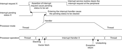
Most peripherals developed for ARM processors use level trigger interrupt output. When an interrupt event take place, the interrupt signal connect from the peripheral to the NVIC will be asserted. The signal will remain high until the processor clears the interrupt request at the peripheral during the interrupt service routine. Inside the NVIC, the pending status register of the interrupt is set when the interrupt is detected and is cleared as the processor accepts and starts the interrupt service routine execution (Figure 9.2).
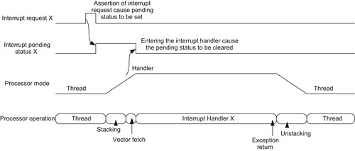
Some interrupt sources might generate interrupt requests in the form of a pulse (for at least one clock cycle). In this case, the pending status register will hold the request until the interrupt is being served (Figure 9.3).
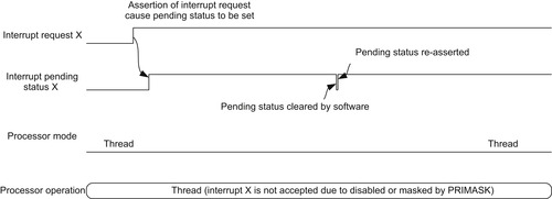
If the interrupt request is not carried out immediately and is de-asserted, and the pending status is cleared by software, then the interrupt request will be ignored and the processor will not execute the interrupt handler (Figure 9.4). The pending status can be cleared by writing to the NVIC CLRPEND register. This is often necessary when setting up a peripheral, and the peripheral might have generated a spurious interrupt request previously.

If the interrupt request is still asserted by the peripheral when the software clears the pending status, the pending status will be asserted again immediately (Figure 9.5).
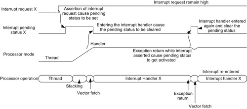
Now let us go back to the normal interrupt processing scenarios. If the interrupt request from the peripheral is not cleared during the execution of the exception handler, the pending status will be activated again at the exception return and will cause the exception handler to be executed again. This might happen if the peripheral got more data to be processed (for example, a data receiver might want to hold the interrupt request high, as long as data remain in its received data FIFO) (Figure 9.6).
 |
| Figure 9.6 |
For pulsed interrupts, if the interrupt request is pulsed several times before the processor starts the interrupt service routine (for example, the processor could be handling another interrupt request), then the multiple interrupt pulses will be treated as just one interrupt request (Figure 9.7).

If the pulsed interrupt request is triggered again during the execution of the interrupt service routine, it will be processed as a new interrupt request and will cause the interrupt service routine to be entered again after the interrupt exit (Figure 9.8).
 |
| Figure 9.8 |
The second interrupt request does not cause the interrupt to be serviced immediately because it is at the same priority level as the current execution priority. Once the processor exits the handler, then the current priority level is lowered, thus allowing the pending interrupt request to be serviced.
The pending status of an interrupt can be activated even when the interrupt is disabled. Therefore, when reprogramming a peripheral and setting up its interrupt and if the previous state of the peripheral is unknown, you might need to clear its interrupt pending status in the NVIC before reenabling the interrupt in the NVIC. This can be done by writing to the Interrupt Clear Pending register in address 0xE000E280.
Interrupt Latency
Under normal situations, the interrupt latency of the Cortex-M0 processor is 16 cycles. The interrupt latency is defined as from the processor clock cycle the interrupt is asserted, to the start of the execution of the interrupt handler. This interrupt latency assumes the following:
• The interrupt is enabled and is not masked by PRIMASK or other executing exception handlers.
• The memory system does not have any wait state. If the memory system has wait state, the interrupt could be delayed by wait states that occur at the last bus transfer before interrupt processing, stacking, vector fetch, or instruction fetch at the start of the interrupt handler.
There are some situations that can result in different interrupt latency:
•
Tail chaining of interrupt. If the interrupt request occurs just as another exception handler returns, the unstacking and stacking process can be skipped, thus reducing the interrupt latency.
•
Late arrival. If the interrupt request occurs during the stacking process of another lower-priority interrupt, the late arrival mechanism allows the new high-priority intercept to take place first. This can result in lower latency for the higher-priority interrupt.
These two behaviors allow interrupt latency to be reduced to a minimum. However, in some embedded applications, zero jitter interrupt response is required. Fortunately, the Cortex-M0 processor is equipped with a zero jitter feature.
On the interface of the Cortex-M0 processor, there is an 8-bit signal called IRQLATENCY, which is connected to the NVIC. This signal can be used to control the interrupt latency behavior. If this signal is connected to a 0, then the Cortex-M0 processor will start to process the interrupt request as soon as possible. If the signal is set to a specific value depending on the timing of the memory system, then it can enable the zero jitter behavior to force the interrupt latency to a higher number of cycles, but it is guaranteed to have zero jitter. The IRQLATENCY signal is normally controlled by configurable registers developed by microcontroller vendors and is not visible on the microcontroller interface.
Control Registers for System Exceptions
Besides the external interrupts, some of the system exceptions can also have programmable priority levels and pending status registers. First, we will look at the priority level registers for system exceptions. On the Cortex-M0 processor, only the three OS-related system exceptions have programmable priority levels. These include SVC, PendSV, and SysTick. Other system exceptions, like NMI and hard fault, have fixed priority levels (Figure 9.9).
The unimplemented bits are read as zero. Write to those unimplemented bits are ignored. On the Cortex-M0 processor, only the System Handler Priority Register 2 (SHPR2) and SHPR3 are implemented (Table 9.4). SHPR1 is not available on the Cortex-M0 processor (it is available on the ARMv7-M architecture—for example, the Cortex-M3 processor).
Users of CMSIS-compliant device drivers can access to the SHPR2 and SHPR3 registers using the register names shown in Table 9.5.
Another NVIC register useful for system exception handling is the Interrupt Control State Register (ISCR) (Table 9.6). This register allows the NMI exception to be pended by software, and it accesses the pending status of PendSV and SysTick exceptions. This register also provides information useful for the debugger, such as the current active exception number and whether or not any exception is currently pended. Because the SysTick implementation is optional, the SysTick exception pending set/clear bits are only available when the SysTick option is presented. As a result, bits 26 and 25 of this register might not be available.
Users of the CMSIS-compliant device driver library can access ICSR using the register name “SCB->ICSR.”
Some of the fields (e.g., the ISRPREEMPT and ISRPENDING fields) in the ICSR are used by the debug system only. In most cases, application code only uses the ICSR to control or check the system exception pending status.
System Control Registers
The NVIC address range (from 0xE000E000 to 0xE000EFFF) also covers a number of system control registers. Therefore, the whole memory range for NVIC is referred to as the System Control Space (SCS). A few of these registers are for the SysTick timer; they will be introduced in the next chapter, where the OS supporting features will be covered. Here the rest of the system control registers are introduced.
CPU ID Base Register
The CPU ID Base register is a read-only register containing the processor ID (Figure. 9.10). It allows application software as well the debugger to determine the processor core type and version information.

The current release of the Cortex-M0 processor (r0p0) has CPU ID values of 0x410CC200. The variant (bit[23:20]) or revision numbers (bit[3:0]) advance for each new release of the core. The CPUID register can be accessed with CMSIS-compliant device drivers such as “SCB->CPUID” (Table. 9.7).
Software can also use this register to determine the CPU type. Bit[7:4] of the CPUID is “0” for the Cortex-M0, “1” for Cortex-M1, “3” for Cortex-M3, and “4” for Cortex-M4.
Application Interrupt and Reset Control Register
The Application Interrupt and Reset Control Register (AIRCR) has several functions (Table. 9.8). It allows an application to request a system reset, determine the endianness of the system, and clear all exception active statuses (this can be done by the debugger only). It can be accessed in CMSIS-compliant device drivers such as “SCB->AIRCR.”
The VECTKEY field is used to prevent accidental write to this register from resetting the system or clearing of the exception status.
The application can use the ENDIANNESS bit as well as the debugger to determine the endianness of the system. This endianness of a Cortex-M0 processor system cannot be changed, as the setup is defined by the microcontroller vendor.
The SYSRESETREQ bit is used to request a system reset. When a value of 1 is written to this bit with a valid key, it causes a signal called SYSRESETREQ on the processor to be asserted. The actual reset timing of the system depends on how this signal is connected. There can be a small delay from the time this bit is written to the actual reset, depending on the design of the system reset control. In typical microcontroller design, the SYSRESETREQ generates system reset for the processor and most parts of the system, but it should not affect the debug system of the microcontroller. This allows the debug operation to work correctly even when the software triggers a reset.
To reset the system using the AIRCR register, you can use the CMSIS function:
void NVIC_SystemReset(void);
Alternatively, the following code can be used:
__DSB(); // Data Synchronization Barrier (include for portability)
// Ensure all memory accessed are completed
__disable_irq(); // Disable interrupts
∗((volatile unsigned long ∗)(0xE000ED0C))=0x05FA0004;//System reset
while(1); // dead loop, waiting for reset
The “while” loop after the write prevents the processor from executing more instructions after the reset request has been issued. The disabling of interrupt is optional; if an interrupt is generated when the system reset request is set, and if the actual reset is delayed because of the reset controller design, there is a chance that the processor will enter the exception handler as the system reset starts. In most cases, it is not an issue, but we can prevent this from happening by setting the exception mask register PRIMASK to disable interrupts before setting the SYSRESETREQ bit.
The use of the DSB instruction allows the code to be used with other ARM processors that have write buffers in the memory interface. In these processors, a memory write operation might be delayed, and if the system reset and memory write happened at the same time, the memory could become corrupted. By inserting a DSB, we can make sure the reset will not happen until the last memory access is completed. Although this is not required in the Cortex-M0 (because there is no write buffer in the Cortex-M0), the DSB is included for better software portability.
The same reset request code can be written in assembly. In the following example code, the step to setting up PRIMASK is optional:
DSB; Data Synchronization Barrier
CPSIDi; Set PRIMASK
LDRR0,=0xE000ED0C ; AIRCR register address
LDRR1,=0x05FA0004 ; Set System reset request
STRR1,[R0]; write back value
Loop
BLoop; dead loop, waiting for reset
The debugger uses the VECTCLRACTIVE bit to clear exception status—for example, when the debugger tries to rerun a program without resetting the processor. Application code running on the processor should not use this feature.
Configuration and Control Register
The Configuration and Control Register (CCR) in the Cortex-M0 processor is a read-only register (Table. 9.9). It determines the double word stack alignment behavior and the trapping of unaligned access. On the ARMv6-M architecture, such as the Cortex-M0 processor, these behaviors are fixed and not configurable. This register is included to make it compatible to ARMv7-M architecture such as the Cortex-M3 processor. On the Cortex-M3 processor, these two behaviors are controllable.
The STKALIGN bit is set to 1, indicating that when exception stacking occurs, the stack frame is always automatically aligned to a double-word-aligned memory location. The UNALIGN_TRP bit is set to 1, indicating that when an instruction attempts to carry out an unaligned transfer, a fault exception will result. Users of CMSIS-compliant device drivers can access to the Configuration Control Register using the register name “SCB->CCR.”
..................Content has been hidden....................
You can't read the all page of ebook, please click here login for view all page.