
Chapter 7. Memory System
Overview
In this chapter we will look into the memory architecture of the Cortex-M0 processor and how it affects software development.
The Cortex-M0 processor has a 32-bit system bus interface with 32-bit address lines (4 GB of address space). The system bus is based on a bus protocol called AHB-Lite (Advanced High-performance Bus), which is a protocol defined in the Advanced Microcontroller Bus Architecture (AMBA) standard. The AMBA standard is developed by ARM, and is widely used in the semiconductor industry.
Although the AHB-Lite protocol provides high-performance accesses to the memory system, very often a secondary bus segment can also be found for slower devices including peripherals. In ARM microcontrollers, the peripheral bus system is normally based on the Advanced Peripheral Bus (APB) protocol. The APB is connected to the AHB-Lite via a bus bridge and may run at a different clock speed compared to the AHB system bus. The data path on the APB is also 32-bit, but the address lines are often less than 32-bit as the peripheral address space is relatively small (Figure 7.1).
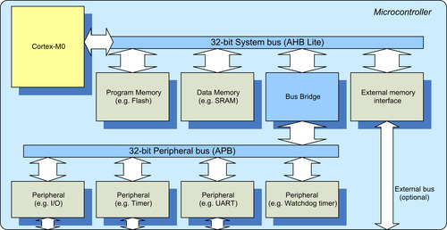
Because of the separation of main system bus and peripheral bus, and in some cases with separated clock frequency controls, an application might need to initialize some clock control hardware in the microcontroller before accessing the peripherals. In some cases, there can be multiple peripheral bus segments in a microcontroller running at different clock frequencies. Besides allowing some part of the system to run at a slower speed, the separation of bus segments also provides the possibility of power reduction by allowing the clock to a peripheral system to be stopped.
Depending on the microcontroller design, some high-speed peripherals might be connected to the AHB-Lite system bus instead of the APB. This is because the AHB-Lite protocol requires fewer clock cycles for each transfer when compared to the APB. The bus protocol behavior affects the system operation and the programmer’s view on the memory system in a number of ways. This subject will be covered in various places in this chapter.
Memory Map
The 4GB memory space of the Cortex-M0 processor is architecturally divided into a number of regions (Figure 7.2). Each region has its recommended usage, and the memory access behavior could depend on which memory region you are accessing to. This memory region definition helps software porting between different ARM Cortex microcontrollers, as they all have similar arrangements.

Despite having an architecturally defined memory map, the actual usage of the memory map is very flexible. There are only a few limitations—for example, a few memory regions that are allocated for peripherals do not allow program code execution, and a number of internal components have a fixed memory address to ensure software portability.
Next we will look into the usage of each region.
Code Region (0x00000000–0x1FFFFFFF)
The size of the code region is 512 MB. It is primarily used to store program code, including the exception vector table, which is a part of the program image. It can also be used for data memory (connection to RAM).
SRAM Region (0x20000000–0x3FFFFFFF)
The SRAM region is the located in the next 512 MB of the memory map. It is primarily used to store data, including stack. It can also be used to store program code. For example, in some cases you might want to copy program code from slow external memory to the SRAM and execute it from there. Despite the name given to this region (it is called “SRAM”), the actual memory devices being used could be SRAM, SDRAM, or some other type.
Peripheral Region (0x40000000–0x5FFFFFFF)
The peripheral region also has the size of 512 MB. It is primarily used for peripherals and can also be used for data storage. However, program execution is not allowed in the peripheral region. The peripherals connected to this memory region can be either the AHB-Lite peripheral or APB peripherals (via a bus bridge).
RAM Region (0x60000000–0x9FFFFFFF)
The RAM region consists of two 512 MB blocks, which results in total of 1 GB of space. Both 512 MB memory blocks are primarily used to stored data, and in most cases the RAM region can be used as a 1GB continuous memory space. The RAM region can also be used for program code execution. The only differences between the two halves of the RAM region is the memory attributes, which might cause differences in cache behavior if a system-level cache (level-2 cache) is used. Memory attributes will be covered in more detail later in this chapter.
Device Region (0xA0000000–0xDFFFFFFF)
The external device region consists of two 512 MB memory blocks, which results in a total of 1 GB of space. Both 512 MB memory blocks are primarily used for peripherals and I/O usage. The device region does not allow program execution, but it can be used for general data storage. Similar to the RAM region, the two halves of the device region have different memory attributes.
Internal Private Peripheral Bus (PPB) (0xE0000000–0xE00FFFFF)
The internal PPB memory space is allocated for peripherals inside the processor, such as the interrupt controller NVIC, as well as the debug components. The internal PPB memory space is 1 MB in size, and program execution is not allowed in this memory range.
Within the PPB memory range, a special range of memory is defined as the System Control Space (SCS). The SCS address is from 0xE000E000 to 0xE000EFFF. It contains the interrupt control registers, system control registers, debug control registers, and the like. The NVIC registers are part of the SCS memory space. The SCS also contains an optional timer called the SysTick. This will be covered in Chapter 10.
Reserved Memory Space (0xE0100000–0xFFFFFFFF)
The last section of the memory map is a 511 MB reserved memory space. This may be reserved in some microcontrollers for vendor-specific usages.
Although the Cortex-M0 processor has this fixed memory map, the memory usage is very flexible. For example, it can have multiple SRAM memory blocks placed in the SRAM region as well as the CODE region, and it can execute program code from external memory components located in RAM region. Microcontroller vendors can also add their own system-level memory features, such as system-level cache, if needed.
So how does the memory map of a typical real system look like? For a typical microcontroller developed with the Cortex-M0 processor, normally you can find the following elements:
• Flash memory (for program code)
• Internal SRAM (for data)
• Internal peripherals
• External memory interface (for external memories as well as external peripherals (optional))
• Interfaces for other external peripherals (optional)
After putting all these components together, an example microcontroller could be illustrated as shown in Figure 7.3.
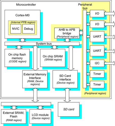
Figure 7.3 shows how some memory regions can be used. However, in many low-cost microcontrollers, the system designs do not have any external memory interface or Secure Digital (SD) card interface. In these cases, some of the memory regions, like the external RAM or the external device regions, might not be used.
Program Memory, Boot Loader, and Memory Remapping
Usually the program memory of the Cortex-M0 is implemented with on chip flash memory. However, it is also possible that the program is stored externally or using other types of memory devices (e.g. EEPROM).
When the Cortex-M0 processor comes out of reset, it accesses the vector table in address zero for initial MSP value and reset vector value, and it then starts the program execution from the reset vector. To ensure that the system works correctly, a valid vector table and a valid program memory must be available in the system to prevent the processor from executing rogue program code.
Usually this is done by a flash memory starting from address zero. However, an off-the-shelf microcontroller product might not have any program in the flash memory before the user programs it. To allow the processor to start up correctly, some Cortex-M0 based microcontrollers come with a boot loader, a small program located on the microcontroller chip that executes after the processor powers up and branches to the user application in the flash memory only if the flash is programmed. The boot loader is preprogrammed by the chip manufacturer. Sometimes it is stored on the on-chip flash memory with a separate memory section from user applications (to allow the user to update the program without affecting the boot loader); other times is it stored on a nonvolatile memory that is separate from the user programmable flash memory (to prevent the users from accidentally erasing the boot loader).
When a boot loader is present, it is common for the microcontroller vendor to implement a memory map-switching feature called “remap” on the system bus. The switching of the memory map is controlled by a hardware register, which is programmed when the boot loader is executed. There are various types of remap arrangements. One common remap arrangement is to allow the boot loader to be mapped to the start of the memory during the power-up phase using address alias, as shown in Figure 7.4.
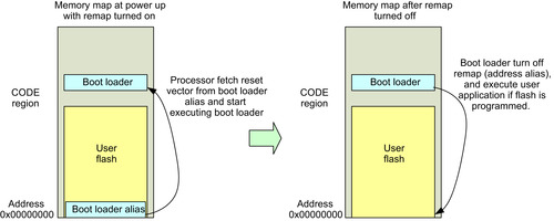
The boot loader might also support additional features like hardware initialization (clock and PLL setup), supporting of multiple boot configurations, firmware protection, or even flash erase utilities. The memory remap feature is implemented on the system bus and is not a part of the Cortex-M0 processor, therefore different microcontrollers from different vendors have different implementations.
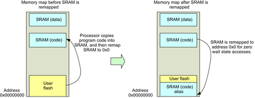
Another common type of remap feature implemented on some ARM microcontrollers allows an SRAM block to be remapped to address 0x0 (Figure 7.5). Normally nonvolatile memory used on microcontrollers like flash memory is slower than SRAM. When the microcontroller is running at a high clock rate, wait states would be required if the program is executed from the flash memory. By allowing an SRAM memory block to be remapped to address 0x0, then the program can be copied to SRAM and executed at maximum speed. This also avoids wait states in vector table fetch, which affects interrupt latency.
Data Memory
The data memory in Cortex-M0 processor is used for software variables, stack memory, and, in some cases, heap memory. Sometimes local variables in C functions could be stored onto the stack memory. The heap memory is needed when the applications use C functions that require dynamically allocated memory space.
In most embedded applications without operating systems (OSs), only one stack is used (only the main stack pointer is required). In this case, the data memory can be arranged as shown in (Figure 7.6).
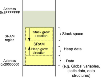
Because the stack operation is based on a full descending stack arrangement, and heap memory allocation is ascending, it is common to put the stack at the end of the memory block and heap memory just after normal memory to get the most efficient arrangement.
For embedded applications with embedded OS, each task might have its own stack memory range (see Figure 4.15 from Chapter 4). It is also possible for each task to have its own allocated memory block, with each memory block containing a memory layout consisting of stack, heap, and data.
Little Endian and Big Endian Support
The Cortex-M0 processor supports either the little endian or big endian memory format (Figure 7.7 and Figure 7.8). The microcontroller vendor makes the choice when the system is designed, and embedded programmers cannot change it. Software developers must configure their development tools project options to match the endianness of the targeted microcontroller.
The big endian mode supported on the Cortex-M0 processor is called the Byte-Invariant big endian mode, or “BE8.” It is one of the big endian modes in ARM architectures. Traditional ARM processors, like ARM7TDMI, use a different big endian mode called the Word-Invariant big endian mode, or “BE32.” The difference between the two is on the hardware interface level and does not affect the programmer’s view.
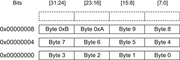
Most of the Cortex-M0 processor–based microcontrollers are using the little endian configuration. With the little endian arrangement, the lowest byte of a word-size data is stored in bit 0 to bit 7 (Figure 7.7).
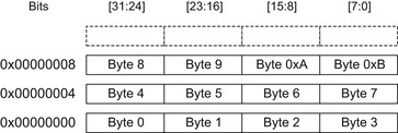
In the big endian configuration, the lowest byte of a word-size data is stored in bit 24 to bit 31 (Figure 7.8)
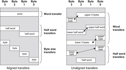
Both memory configurations support data handling of different sizes. The Cortex-M0 processor can generate byte, half-word, and word transfers. When the memory is accessed, the memory interface selects the data lanes base on the transfer size and the lowest two bits of the address. Figure 7.9 illustrates the data access for little endian systems.

Similarly, a big endian system supports data access of different sizes (Figure 7.10).
Note that there are two exceptions in big endian configurations: (1) the instruction fetch is always in little endian, and (2) the accesses to Private Peripheral Bus (PPB) address space is always in little endian.
Data Type
The Cortex-M0 processor supports different data types by providing various memory access instructions for different transfer sizes and by providing a 32-bit AHB-LITE interface, which supports 32-bit, 16-bit, and 8-bit transfers. For example, in C language development, the data types presented in Table 7.1 are commonly used.
If “stdint.h” in C99 is used, the data types shown in Table 7.2 are available.
For other data types that require a larger size (e.g., int64_t, uint64_t), the C compilers automatically convert the data transfer into multiple memory access instructions.
Note that for peripheral register accesses, the data type being used should match the hardware register size. Otherwise the peripheral might ignore the transfer or not functioning as expected. In most cases, peripherals connected to the peripheral bus (APB) should be accessed using word-size transfers. This is because APB protocol does not have transfer size signals, hence all the transfers are assumed to be word size. Therefore, peripheral registers accessed via the APB are normally declared to be “volatile unsigned integers.”
Effect of Hardware Behavior to Programming
The design of the processor hardware and the behavior of the bus protocol affect the software in a number of ways. In a previous section, we mentioned that peripherals connected to the APB are usually accessed using word-size transfers because of the nature of the APB protocol. In this section, we will look into other similar aspects.
Data Alignment
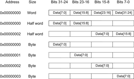
The Thumb instruction set supported by the Cortex-M0 processor can only generate aligned transfers (Figure 7.11). It means that the transfer address must be a multiple of the transfer size. For example, a word size transfer can only access addresses like 0x0, 0x4, 0x8, 0xC, and so forth. Similarly, a half-word transfer can only access addresses like 0x0, 0x2, 0x4, and so forth. All byte data accesses are aligned.
If the program attempts to generate an unaligned transfer, this will result in a fault exception and cause the hard fault handler to be executed. In normal cases, C compilers do not generate any unaligned transfers, but an unaligned transfer can still be generated if a C program directly manipulated a pointer.
Unaligned transfers can also be generated accidentally when programming in assembly language—for example, when load store instructions of wrong transfer size is used. In the case of a half-word data type located in address 0x1002, which is an aligned data type, it can be accessed using LDRH, LDRSH, or STRH instructions without problems. But if the program code used LDR or STR instruction to access the data, an unaligned access fault would be triggered.
Access to Invalid Addresses
Unlike most 8-bit or 16-bit processors, a memory access to an invalid memory address generates a fault exception on ARM Cortex-M0 microcontrollers. This provides better program error detection and allows software bugs to be detected earlier.
In the AHB system connected to the Cortex-M0 processor, the address decoding logic detects the address being accessed and the bus system response with an error signal if the access is going to an invalid location. The bus error can be caused by either data access or instruction fetch.
One exception to this behavior is the branch shadow instruction fetch. Because of the pipeline nature of the Cortex-M0 processor, instructions are fetched in advanced. Therefore, if the program execution reaches the end of a valid memory region and a branch is executed, there might be chance that the addresses beyond the valid instruction memory region could have been fetched, resulting in a bus fault in the AHB system. However, in this case the bus fault would be ignored if the faulted instruction is not executed because of the branch.
Use of Multiple Load and Store Instructions
The multiple load and store instructions in the Cortex-M0 processor can greatly increase the system performance when used correctly. For example, it can be used to speed up data transfer processes or as a way to adjust the memory pointer automatically.
When handling peripheral accesses, we need to avoid the use of LDM or STM instructions. If the Cortex-M0 processor receives an interrupt request during the execution of LDM or STM instructions, the LDM or STM instruction will be abandoned and the interrupt service will be initiated. At the end of the interrupt service, the program execution will return to the interrupted LDM or STM instruction and restart from the
first transfer of the interrupted LDM or STM.
As a result of this restart behavior, some of the transfers in this interrupt LDM or STM instruction could be carried out twice. It is not a problem for normal memory devices, but if the access is carried on a peripheral, then the repeating of the transfer could cause error. For example, if the LDM instruction is used for reading a data value in a First-In-First-Out (FIFO) buffer, then some of the data in the FIFO could be lost as the read operation is repeated.
As a precaution, we should avoid the use of LDM or STM instructions on peripheral accesses unless we are sure that the restart behavior does not cause incorrect operation to the peripheral.
Memory Attributes
The Cortex-M0 processor can be used with wide range of memory systems and devices. To make porting of software between different devices easier, a number of memory attribute settings are available for each region in the memory map. Memory attributes are characteristics of the memory accesses; they can affect data and instruction accesses to memory as well as accesses to peripherals.
In the ARMv6-M architecture, which is used by the Cortex-M0 processor, a number of memory access attributes are defined for different memory regions:
•
Executable. The shareable attribute defines whether program execution is allowed in that memory region. If a memory region is define as nonexecutable, in ARM documentation it is marked as eXecute Never (XN).
•
Bufferable. When a data write is carried out to a bufferable memory region, the write transfer can be buffered, which means the processor can continue to execute the next instruction without waiting for the current write transfer to complete.
•
Cacheable. If a cache device is present on the system, it can keep a local copy of the data during a data transfer and reuse it the next time the same memory location is accessed to speed up the system. The cache device can be a cache memory unit or a small buffer in a memory controller.
•
Shareable. The shareable attribute defines whether more than one processor can access a shareable memory region. If a memory region is shareable, the memory system needs to ensure coherency between memory accesses by multiple processors in this region.
For most users of the Cortex-M0 products, only the XN attribute is relevant because it defines which regions can be used for program execution. The other attributes are used only if cache unit or multiple processors are used. Because the Cortex-M0 processor does not have an internal cache unit, in most cases these memory attributes are not used. If a system-level cache is used or when the memory controller has a built-in cache, then these memory attributes, exported by the processor via the AHB interface, could be used.
Based on the memory attributes, various memory types are architecturally defined and are used to define what type of devices could be used in each memory region:
•
Device memory. Device memories are noncacheable. They can be shareable or nonshareable.
•
Strongly-ordered (SO) memory. A memory region that is nonbufferable, noncacheable, and transfers to/from a strongly ordered region takes effect immediately. Also, the orders of strongly ordered transfers on the memory interface must be identical to the orders of the corresponding memory access instructions (no access reordering for speed optimization; the Cortex-M0 does not have any access reordering feature). Strongly ordered memory regions are always shareable.
The memory attribute for each memory region in the Cortex-M0 processor is defined using these memory type definitions (Table 7.3). During the memory accesses, the memory attributes are exported from the processor to the AHB system.
The PPB memory region is defined as strongly ordered (SO). This means the memory region is nonbufferable and noncacheable. In the Cortex-M0, operations following an access to a strongly order region do not begin until the access has been completed. This behavior is important for changing registers in the System Control Space (SCS), where we often expect the operation of changing a control register to take place immediately, before next instruction is executed.
In some other ARM processors like the Cortex-M3, there can also be default memory access permission for each region. Because the Cortex-M0 processor does not have a separated privileged and nonprivileged (user) access level, the processor is in the privilege access level all the time and therefore does not have a memory map for default memory access permission.
In practice, most of the memory attributes and memory type definitions are unimportant (apart from the XN attribute) to users of Cortex-M0 microcontrollers. However, if the software code has to be reused on high-end processors, especially on systems with multiple processors and cache memories, these details can be important.
..................Content has been hidden....................
You can't read the all page of ebook, please click here login for view all page.