
Chapter 3. Architecture
Overview
The ARMv6-M architecture that the Cortex-M0 processor implemented covers a number of different areas. The complete details of the ARMv6-M architecture are documented in the ARMv6-M Architecture Reference Manual [reference 3]. This document is available from the ARM web site via a registration process. However, you do not have to know the complete details of the architecture to start using a Cortex-M0 microcontroller. To use a Cortex-M0 device with C language, you only need to know the memory map, the peripheral programming information, the exception handling mechanism, and part of the programmer’s model.
In this chapter, we will cover the programmer’s model and a basic overview of the memory map and exceptions. Most users of the Cortex-M0 processor will work in C language; as a result, the underlying programmer’s model will not be visible in the program code. However, it is still useful to know about the details, as this information is often needed during debugging and it will also help readers to understand the rest of this book.
Programmer’s Model
Operation Modes and States
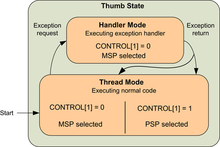
The Cortex-M0 processor has two operation modes and two states (Figure 3.1).

When the processor is running a program, it is in the Thumb state. In this state, it can be either in the Thread mode or the Handler mode. In the ARMv6-M architecture, the programmer’s model of Thread mode and Handler mode are almost completely the same. The only difference is that Thread mode can use a shadowed stack pointer (Figure 3.7, presented later in the chapter) by configuring a special register called CONTROL. Details of stack pointer selection are covered later in this chapter.
The Debug state is used for debugging operation only. Halting the processor stops the instruction execution and enter debug state. This state allows the debugger to access or change the processor register values. The debugger can access system memory locations in either the Thumb state or the Debug state.
When the processor is powered up, it will be running in the Thumb state and Thread mode by default.
Registers and Special Registers
To perform data processing and controls, a number of registers are required inside the processor core. If data from memory are to be processed, they have to be loaded from the memory to a register in the register bank, processed inside the processor, and then written back to the memory if needed. This is commonly called a “load-store architecture.” By having a sufficient number of registers in the register bank, this mechanism is easy to use and is C friendly. It is easy for C compilers to compile a C program into machine code with good performance. By using internal registers for short-term data storage, the amount of memory accesses can be reduced.
The Cortex-M0 processor provides a register bank of 13 general-purpose 32-bit registers and a number of special registers (Figure 3.2).

The register bank contains sixteen 32-bit registers. Most of them are general-purpose registers, but some have special uses. The detailed descriptions for these registers are as follows.
R0–R12
Registers R0 to R12 are for general uses. Because of the limited space in the 16-bit Thumb instructions, many of the Thumb instructions can only access R0 to R7, which are also called the low registers, whereas some instructions, like MOV (move), can be used on all registers. When using these registers with ARM development tools such as the ARM assembler, you can use either uppercase (e.g., R0) or lowercase (e.g., r0) to specify the register to be used. The initial values of R0 to R12 at reset are undefined.
R13, Stack Pointer (SP)
R13 is the stack pointer. It is used for accessing the stack memory via PUSH and POP operations. There are physically two different stack pointers in Cortex-M0. The main stack pointer (MSP, or SP_main in ARM documentation) is the default stack pointer after reset, and it is used when running exception handlers. The process stack pointer (PSP, or SP_process in ARM documentation) can only be used in Thread mode (when not handling exceptions). The stack pointer selection is determined by the CONTROL register, one of the special registers that will be introduced later.
When using ARM development tools, you can access the stack pointer using either “R13” or “SP.” Both uppercase and lowercase (e.g., “r13” or “sp”) can be used. Only one of the stack pointers is visible at a given time. However, you can access to the MSP or PSP directly when using the special register access instructions MRS and MSR. In such cases, the register names “MSP” or “PSP” should be used.
The lowest two bits of the stack pointers are always zero, and writes to these two bits are ignored. In ARM processors, PUSH and POP are always 32-bit accesses because the registers are 32-bit, and the transfers in stack operations must be aligned to a 32-bit word boundary. The initial value of MSP is loaded from the first 32-bit word of the vector table from the program memory during the startup sequence. The initial value of PSP is undefined.
R14, Link Register (LR)
R14 is the Link Register. The Link Register is used for storing the return address of a subroutine or function call. At the end of the subroutine or function, the return address stored in LR is loaded into the program counter so that the execution of the calling program can be resumed. In the case where an exception occurs, the LR also provides a special code value, which is used by the exception return mechanism. When using ARM development tools, you can access to the Link Register using either “R14” or “LR.” Both upper and lowercase (e.g., “r14” or “lr”) can be used.
Although the return address in the Cortex-M0 processor is always an even address (bit[0] is zero because the smallest instructions are 16-bit and must be half-word aligned), bit zero of LR is readable and writeable. In the ARMv6-M architecture, some instructions require bit zero of a function address set to 1 to indicate Thumb state.
R15, Program Counter (PC)
R15 is the Program Counter. It is readable and writeable. A read returns the current instruction address plus four (this is caused by the pipeline nature of the design). Writing to R15 will cause a branch to take place (but unlike a function call, the Link Register does not get updated).
In the ARM assembler, you can access the Program Counter, using either “R15” or “PC,” in either upper or lower case (e.g., “r15” or “pc”). Instruction addresses in the Cortex-M0 processor must be aligned to half-word address, which means the actual bit zero of the PC should be zero all the time. However, when attempting to carry out a branch using the branch instructions (BX or BLX), the LSB of the PC should be set to 1. 2 This is to indicate that the branch target is a Thumb program region. Otherwise, it can imply trying to switch the processor to ARM state (depending on the instruction used), which is not supported and will cause a fault exception.
xPSR, combined Program Status Register
The combined Program Status Register provides information about program execution and the ALU flags. It is consists of the following three Program Status Registers (PSRs) (Figure 3.3):
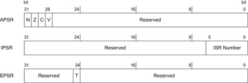
• Application PSR (APSR)
• Interrupt PSR (IPSR)
• Execution PSR (EPSR)
The APSR contains the ALU flags: N (negative flag), Z (zero flag), C (carry or borrow flag), and V (overflow flag). These bits are at the top 4 bits of the APSR. The common use of these flags is to control conditional branches.
The IPSR contains the current executing interrupt service routine (ISR) number. Each exception on the Cortex-M0 processor has a unique associated ISR number (exception type). This is useful for identifying the current interrupt type during debugging and allows an exception handler that is shared by several exceptions to know what exception it is serving.
The EPSR on the Cortex-M0 processor contains the T-bit, which indicates that the processor is in the Thumb state. On the Cortex-M0 processor, this bit is normally set to 1 because the Cortex-M0 only supports the Thumb state. If this bit is cleared, a hard fault exception will be generated in the next instruction execution.
These three registers can be accessed as one register called xPSR (Figure 3.4). For example, when an interrupt takes place, the xPSR is one of the registers that is stored onto the stack memory automatically and is restored automatically after returning from an exception. During the stack store and restore, the xPSR is treated as one register.

Direct access to the Program Status Registers is only possible through special register access instructions. However, the value of the APSR can affect conditional branches and the carry flag in the APSR can also be used in some data processing instructions.
Behaviors of the Application Program Status Register (APSR)
Data processing instructions can affect destination registers as well as the APSR, which is commonly known as ALU status flags in other processor architectures. The APSR is essential for controlling conditional branches. In addition, one of the APSR flags, the C (Carry) bit, can also be used in add and subtract operations.
There are four APSR flags in the Cortex-M0 processor, and they are identified in Table 3.1.
A few examples of the ALU flag results are shown in Table 3.2.
In the Cortex-M0, almost all of the data processing instructions modify the APSR; however, some of these instructions do not update the V flag or the C flag. For example, the MULS (multiply) instruction only changes the N flag and the Z flag.
The ALU flags can be used for handling data that is larger than 32 bits. For example, we can perform a 64-bit addition by splitting the operation into two 32-bit additions. The pseudo form of the operation can be written as follows:
// Calculating Z = X + Y, where X, Y and Z are all 64-bit
Z[31:0] = X[31:0] + Z[31:0]; // Calculate lower word addition, carry flag get updated
Z[63:32] = X[63:32] + Z[63:32] + Carry; // Calculate upper word addition
An example of carry out such 64-bit add operation in assembly code can be found in Chapter 6.
The other common usage of APSR flag is to control branching. This topic is addressed in Chapter 4, where the details of the condition branch instruction will be covered.
PRIMASK: Interrupt Mask Special Register
The PRIMASK register is a 1-bit-wide interrupt mask register (Figure 3.5). When set, it blocks all interrupts apart from the nonmaskable interrupt (NMI) and the hard fault exception. Effectively it raises the current interrupt priority level to 0, which is the highest value for a programmable exception.
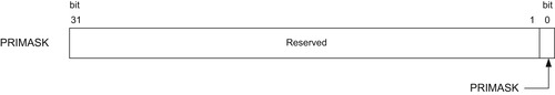
The PRIMASK register can be accessed using special register access instructions (MSR, MRS) as well as using an instruction called the Change Processor State (CPS). This is commonly used for handling time-critical routines.
CONTROL: Special Register
As mentioned earlier, there are two stack pointers in the Cortex-M0 processor. The stack pointer selection is determined by the processor mode as well as the configuration of the CONTROL register (Figure 3.6).
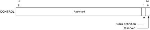
After reset, the main stack pointer (MSP) is used, but can be switched to the process stack pointer (PSP) in Thread mode (when not running an exception handler) by setting bit [1] in the CONTROL register (Figure 3.7). During running of an exception handler (when the processor is in Handler mode), only the MSP is used, and the CONTROL register reads as zero. The CONTROL register can only be changed in Thread mode or via the exception entrance and return mechanism.
Bit 0 of the CONTROL register is reserved to maintain compatibility with the Cortex-M3 processor. In the Cortex-M3 processor, bit 0 can be used to switch the processor to User mode (non-privileged mode). This feature is not available in the Cortex-M0 processor.
Memory System Overview
The Cortex-M0 processor has 4 GB of memory address space (Figure 3.8). The memory space is architecturally defined as a number of regions, with each region having a recommended usage to help software porting between different devices.
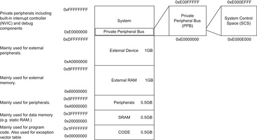
The Cortex-M0 processor contains a number of built-in components like the NVIC and a number of debug components. These are in fixed memory locations within the system region of the memory map. As a result, all the devices based on the Cortex-M0 have the same programming model for interrupt control and debug. This makes it convenient for software porting and helps debug tool vendors to develop debug solutions for the Cortex-M0 based microcontroller or system-on-chip (SoC) products.
In most cases, the memories connected to the Cortex-M0 are 32-bits, but it is also possible to connect memory of different data widths to the Cortex-M0 processor with suitable memory interface hardware. The Cortex-M0 memory system supports memory transfers of different sizes such as byte (8-bit), half word (16-bit), and word (32-bit). The Cortex-M0 design can be configured to support either little endian or big endian memory systems, but it cannot switch from one to another in an implemented design.
Because the memory system and peripherals connected to the Cortex-M0 are developed by microcontroller vendors or system-on-chip (SoC) designers, different memory sizes and memory types can be found in different Cortex-M0 based products.
Stack Memory Operations
Stack memory is a memory usage mechanism that allows the system memory to be used as temporary data storage that behaves as a first-in, last-out buffer. One of the essential elements of stack memory operation is a register called the stack pointer. The stack pointer is adjusted automatically each time a stack operation is carried out. In the Cortex-M0 processor, the stack pointer is register R13 in the register bank. Physically there are two stack pointers in the Cortex-M0 processor, but only one of them is used at one time, depending on the current value of the CONTROL register and the state of the processor (see Figure 3.7).
In common terms, storing data to the stack is called pushing (using the PUSH instruction) and restoring data from the stack is called popping (using the POP instruction). Depending on processor architecture, some processors perform storing of new data to stack memory using incremental address indexing and some use decrement address indexing. In the Cortex-M0 processor, the stack operation is based on a “full-descending” stack model. This means the stack pointer always points to the last filled data in the stack memory, and the stack pointer predecrements for each new data store (PUSH) (Figure 3.9).

PUSH and POP are commonly used at the beginning and end of a function or subroutine. At the beginning of a function, the current contents of the registers used by the calling program are stored onto the stack memory using a PUSH operation, and at the end of the function, the data on the stack memory is restored to the registers using a POP operation. Typically, each register PUSH operation should have a corresponding register POP operation, otherwise the stack pointer will not be able to restore registers to their original values. This can result in unpredictable behavior, for example, stack overflow.
The minimum data size to be transferred for each push and pop operations is one word (32-bit), and multiple registers can be pushed or popped in one instruction. The stack memory accesses in the Cortex-M0 processor are designed to be always word aligned (address values must be a multiple of 4, for example, 0×0, 0×4, 0×8, etc.), as this gives the best efficiency for minimum design complexity. For this reason, bits [1:0] of both stack pointers in the Cortex-M0 processor are hardwired to zeros and read as zeros.
The stack pointer can be accessed as either R13 or SP. Depending on the processor state and the CONTROL register value, the stack pointer accessed can either be the main stack pointer (MSP) or the process stack pointer (PSP). In many simple applications, only one stack pointer is needed and by default the main stack pointer (MSP) is used. The process stack pointer (PSP) is usually only required when an operating system (OS) is used in the embedded application (Table 3.3).
In a typical embedded application with an OS, the OS kernel uses the MSP and the application processes use the PSP. This allows the stack for the kernel to be separate from stack memory for the application processes. This allows the OS to carry out context switching quickly (switching from execution of one application process to another). Even though the OS kernel only uses the MSP as its stack pointer, it can still access the value in PSP by using special register access instructions (MRS and MSR).
Because the stack grows downward (full-descending), it is common for the initial value of the stack pointer to be set to the upper boundary of SRAM. For example, if the SRAM memory range is from 0x20000000 to 0x20007FFF, we can start the stack pointer at 0x20008000. In this case, the first stack PUSH will take place at address 0x20007FFC, the top word of the SRAM.
The initial value of MSP is stored at the beginning of the program memory. Here we will find the exception vector table, which is introduced in the next section. The initial value of PSP is undefined, and therefore the PSP must be initialized by software before using it.
Exceptions and Interrupts
Exceptions are events that cause change to program control: instead of continuing program execution, the processor suspends the current executing task and executes a part of the program code called the exception handler. After the exception handler is completed, it will then resume the normal program execution. There are various types of exceptions, and interrupts are a subset of exceptions. The Cortex-M0 processor supports up to 32 external interrupts (commonly referred as IRQs) and an additional special interrupt called the nonmaskable interrupt (NMI). The exception handlers for interrupt events are commonly known as interrupt service routines (ISRs). Interrupts are usually generated by on-chip peripherals, or by external input through I/O ports. The number of available interrupts on the Cortex-M0 processor depends on the microcontroller product you use. In systems with more peripherals, it is possible for multiple interrupt sources to share one interrupt connection.
Besides the NMI and IRQ, there are a number of system exceptions in the Cortex-M0 processor, primarily for OS use and fault handling (Table 3.4).
Each exception has an exception number. This number is reflected in various registers including the IPSR and is used to define the exception vector addresses. Note that exception number is separated from interrupt numbers used in device driver libraries. In most device driver libraries, system exceptions are defined using negative numbers, and interrupts are defined as positive numbers from 0 to 31.
Reset is a special type of exception. When the Cortex-M0 processor exits from a reset, it executes the reset handler in Thread mode (no need to return from handler to thread). Also, the exception number of 1 is not visible in the IPSR.
Apart from NMI, hard fault, and reset, all other exceptions have a programmable priority level. The priority level for NMI and hard fault are fixed and both have a higher priority than the rest of the exceptions. More details will be covered in Chapter 8.
Nested Vectored Interrupt Controller (NVIC)
To prioritize the interrupt requests and handle other exceptions, the Cortex-M0 processor has a built-in interrupt controller called the Nested Vectored Interrupt Controller (NVIC). The interrupt management function is controlled by a number of programmable registers in the NVIC. These registers are memory mapped, with the addresses located within the System Control Space (SCS) as illustrated in Figure 3.8.
The NVIC supports a number of features:
• Flexible interrupt management
• Nested interrupt support
• Vectored exception entry
• Interrupt masking
Flexible Interrupt Management
In the Cortex-M0 processor, each external interrupt can be enabled or disabled and can have its pending status set or clear by software. It can also accept exception requests at signal level (interrupt request from a peripheral remain asserted until the interrupt service routine clears the interrupt request), as well as an exception request pulse (minimum 1 clock cycle). This allows the interrupt controller to be used with any interrupt source.
Nested Interrupt Support
In the Cortex-M0 processor, each exception has a priority level. The priority level can be fixed or programmable. When an exception occurs, such as an external interrupt, the NVIC will compare the priority of this exception to the current level. If the new exception has a higher priority, the current running task will be suspended. Some of the registers will be stored on to the stack memory, and the processor will start executing the exception handler of the new exception. This process is called “preemption.” When the higher priority exception handler is complete, it is terminated with an exception return operation and the processor automatically restores the registers from the stack and resumes the task that was running previously. This mechanism allows nesting of exception services without any software overhead.
Vectored Exception Entry
When an exception occurs, the processor will need to locate the starting point of the corresponding exception handler. Traditionally, in ARM processors such as the ARM7TDMI, software usually handles this step. The Cortex-M0 automatically locates the starting point of the exception handler from a vector table in the memory. As a result, the delay from the start of the exception to the execution of the exception handlers is reduced.
Interrupt Masking
The NVIC in the Cortex-M0 processor provides an interrupt masking feature via the PRIMASK special register. This can disable all exceptions except hard fault and NMI. This masking is useful for operations that should not be interrupted such as time critical control tasks or real-time multimedia codecs.
The above NVIC features help makes the Cortex-M0 processor easier to use, provides better response times, and reduces program code size by managing the exceptions in the NVIC hardware.
System Control Block (SCB)
Apart from the NVIC, the System Control Space (SCS) also contains a number of other registers for system management. This is called the System Control Block (SCB). It contains registers for sleep mode features and system exception configurations, as well as a register containing the processor identification code (which can be used by in circuit debuggers for detection of the processor type).
Debug System
Although it is currently the smallest processor in the ARM processor family, the Cortex-M0 processor supports various debug features. The processor core provides halt mode debug, stepping, and register accesses, and additional debug blocks provide debug features like the Breakpoint Unit (BPU) and Data Watchpoint (DWT) units. The BPU supports up to four hardware breakpoints, and the DWT supports up to two watchpoints.
To allow a debugger to control the aforementioned debug components and carry out debug operations, the Cortex-M0 processor provides a debug interface unit. This debug interface unit can either use the JTAG protocol or the serial wire debug (SWD) protocol. In some Cortex-M0 products, the microcontroller vendors can also choose to use a debug interface unit, which supports both JTAG and serial wire debug protocol. However, typical Cortex-M0 implementations are likely to support only one protocol with SWD probably being preferred because fewer pins are required.
The serial wire debug protocol is a new standard developed by ARM, and it can reduce the number connection to just two signals. It can handle all the same debug features as JTAG without any loss of performance. The serial wire debug interface shares the same connector as JTAG: The Serial clock signal is shared with JTAG TCK signal, and the serial wire data are shared with the JTAG TMS signal (Figure 3.10). There are many debug emulators for ARM microcontrollers, including ULINK2 (from Keil) and JLink (from SEGGER), that already support the serial wire debug protocol.

Program Image and Startup Sequence
To understand the startup sequence of the Cortex-M0 processor, we need to have a quick overview on the program image first. Normally, the program image for the Cortex-M0 processor is located from address 0x00000000.
The beginning of the program image contains the vector table (Figure 3.11). It contains the starting addresses (vectors) of exceptions. Each vector is located in address of “Exception_Number × 4.” For example, external IRQ #0 is exception type #16, therefore the address of the vector for IRQ#0 is in 16 × 4 = 0×40. These vectors have LSB set to 1 to indicate that the exceptions handlers are to be executed with Thumb instructions. The size of the vector table depends on how many interrupts are implemented.
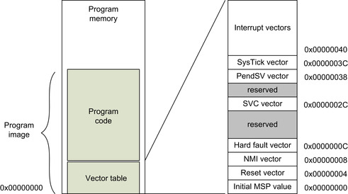
The vector table also defines the initial value of the main stack pointer (MSP). This is stored in the first word of the vector table.
When the processor exits from reset, it will first read the first two-word addresses in the vector table. The first word is the initial MSP value, and the second word is the reset vector (Figure 3.12), which determines the starting of the program execution address (reset handler).

For example, if we have boot code starting from address 0x000000C0, we need to put this address value in the reset vector location with the LSB set to 1 to indicate that it is Thumb code. Therefore, the value in address 0x00000004 is set to 0x000000C1 (Figure 3.13). After the processor fetches the reset vector, it will start executing program code from the address found there. This behavior is different from traditional ARM processors (e.g., ARM7TDMI), where the processor executes the program starting from address 0x00000000, and the vectors in the vector table are instructions as oppose to address values in the Cortex-M processors.
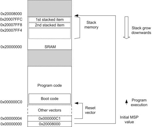
The reset sequence also initializes the main stack pointer (MSP). Assume we have SRAM located from 0x20000000 to 0x20007FFF, and we want to put the main stack at the top of the SRAM; we can set this up by putting 0x20008000 in address 0x00000000 (Figure 3.13).
Because the Cortex-M0 processor will first decrement the stack pointer before pushing the data on to the stack, the first stacked item will be located in 0x200007FFC, which is just at the top of the SRAM, whereas the second stacked item will be in 0x20007FF8, below the first stacked item.
This behavior differs from that of traditional ARM processors and many other microcontroller architectures where the stack pointer has to be initialized by software code rather than a value in a fixed address.
If the process stack pointer (PSP) is to be used, it must be initialized by software code before writing to the CONTROL register to switch the stack pointer. The reset sequence only initializes the MSP and not the PSP.
Different software development tools have different ways of specifying the initial stack pointer value and the values for the reset and exception vectors. Most of the development tools come with code examples demonstrating how this can be done with their development flow. In most compilation tools, the vector table can be defined completely using C.
..................Content has been hidden....................
You can't read the all page of ebook, please click here login for view all page.