
Appendix E. Debug Registers Quick Reference
Overview
The Cortex-M0 debug system contains a number of programmable registers. These registers can be accessed by an in-circuit debuggers only and cannot be accessed by the application software. This quick reference is intended for tools developers, or if you are using a debugger that supports debug scripts (e.g., RealView Debugger), you can use debug scripts to access to these registers to carry out testing operations automatically.
The debug system in the Cortex-M0 is partitioned into the following segments:
• Debug support in the processor core
• Breakpoint unit
• Data watchpoint unit
• ROM table.
System-on-chip developers can add debug support components if required. If additional debug components are added, another ROM table unit can also be added to the system so that a debugger can identify available debug components included in the system.
The debug support is configurable; some Cortex-M0 based products might not have any debug support.
Core Debug Registers
The processor core contains a number of registers for debug purpose.
| Address | Name | Descriptions |
|---|---|---|
| 0xE000ED24 | SHCSR | System Handler Control and State Register—indicate system exception status |
| 0xE000ED30 | DFSR | Debug Fault Status Register—allow debugger to determine the cause of halting |
| 0xE000EDF0 | DHCSR | Debug Halting Control and Status Register—control processor debug activities like halting, single stepping, restart |
| 0xE000EDF4 | DCRSR | Debug Core Register Selector Register—control read and write of core registers during halt |
| 0xE000EDF8 | DCRDR | Debug Core Register Data Register—data transfer register for reading or writing core registers during halt |
| 0xE000EDFC | DEMCR | Debug Exception Monitor Control Register—for enabling of data watchpoint unit and vector catch feature; vector catch allows the debugger to halt the processor if the processor is reset or if a hard fault exception is triggered |
| 0xE000EFD0 to 0xE000EFFC | PIDs, CIDs | ID registers |
| Bits | Field | Type | Reset Value | Descriptions |
|---|---|---|---|---|
| 31:0 | DBGTMP | RW | 0 | Data value for the core register transfer |
Breakpoint Unit
The breakpoint unit contains up to four comparators for instruction breakpoints. Each comparator can produce a breakpoint for up to two instructions (if the two instructions are located in the same word address). Additional breakpoints can be implemented by inserting breakpoint instructions in the program image if the program memory can be modified.
The breakpoint unit design is configurable. Some microcontrollers might contain no breakpoint unit or a breakpoint unit with fewer than four comparators.
| Address | Name | Descriptions |
|---|---|---|
| 0xE0002000 | BP_CTRL | Breakpoint Control Register—for enabling the breakpoint unit and provide information about the breakpoint unit |
| 0xE0002008 | BP_COMP0 | Breakpoint Comparator Register 0 |
| 0xE000200C | BP_COMP1 | Breakpoint Comparator Register 1 |
| 0xE0002010 | BP_COMP2 | Breakpoint Comparator Register 2 |
| 0xE0002014 | BP_COMP3 | Breakpoint Comparator Register 3 |
| 0xE0002FD0 to 0xE0002FFC | PIDs, CIDs | ID registers |
Data Watchpoint Unit
The data watchpoint unit has two main functions:
• Setting data watchpoints
• Providing a PC sampling register for basic profiling
Before accessing the DWT, the TRCENA bit in Debug Exception and Monitor Control Register (DEMCR, address 0xE000EDFC) must be set to 1 to enable the DWT. Unlike the Data Watchpoint and Trace unit in the Cortex-M3/M4, the DWT in the Cortex-M0 does not support trace. But the programming models of its registers are mostly compatible to the DWT in ARMv7-M.
The DWT design is configurable. Some microcontrollers might contain no DWT or a DWT with just 1 comparator.
| Address | Name | Descriptions |
|---|---|---|
| 0xE0001000 | DWT_CTRL | DWT Control Register—provide information about the data watchpoint unit |
| 0xE000101C | DWT_PCSR | Program Counter Sample Register—provide current program address |
| 0xE0001020 | DWT_COMP0 | Comparator Register 0 |
| 0xE0001024 | DWT_MASK0 | Mask Register 0 |
| 0xE0001028 | DWT_FUNCTION0 | Function Register 0 |
| 0xE0001030 | DWT_COMP1 | Comparator Register 1 |
| 0xE0001034 | DWT_MASK1 | Mask Register 1 |
| 0xE0001038 | DWT_FUNCTION1 | Function Register 1 |
| 0xE0001FD0 to 0xE0001FFC | PIDs, CIDs | ID registers |
| Bits | Field | Type | Reset Value | Descriptions |
|---|---|---|---|---|
| 31:28 | NUMCOMP | RO | 0 to 2 | Number of comparator implemented |
| 27:0 | Reserved | — | — | Reserved |
| Bits | Field | Type | Reset Value | Descriptions |
|---|---|---|---|---|
| 31:0 | EIASAMPLE | RO | — | Execution instruction address sample; read as 0xFFFFFFFF if core is halted or if DWTENA is 0 |
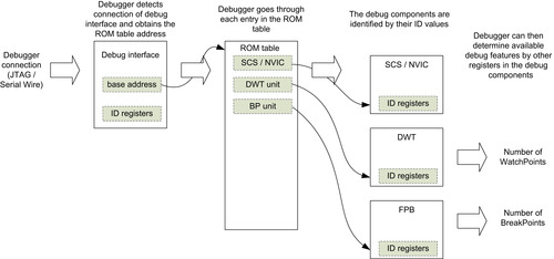
ROM Table Registers
The ROM table is used to allow a debugger to identify available components in the system. The lowest two bits of each entry are used to indicate if the debug component is present and if there is another valid entry following in the next address in the ROM table. The rest of the bits in the ROM table contain the address offset of the debug unit from the ROM table base address:
| Address | Value | Name | Descriptions |
|---|---|---|---|
| 0xE00FF000 | 0xFFF0F003 | SCS | Points to System Control Space base address 0xE000E000 |
| 0xE00FF004 | 0xFFF02003 | DWT | Points to DW base address 0xE0001000 |
| 0xE00FF008 | 0xFFF03003 | BPU | Points to BPU base address 0xE0002000 |
| 0xE00FF00C | 0x00000000 | end | End of table marker |
| 0xE00FFFCC | 0x00000001 | MEMTYPE | Indicates that system memory is accessible on this memory map |
| 0xE00FFFD0 to 0xE00FFFFC | 0x000000-- | IDs | Peripheral ID and component ID values (values dependent on the design versions) |
Using the ROM table, the debugger can identify the debug components available as shown in Figure E.1.
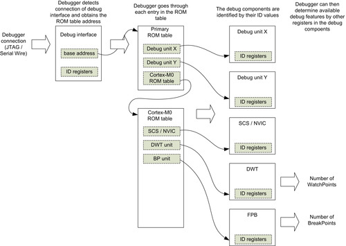
The ROM table lookup can be divided into multiple stages if a system-on-chip design contains additional debug components and an extra ROM table. In such cases, the ROM table lookup can be cascaded so that the debugger can identify all the debug components available (Figure E.2).
..................Content has been hidden....................
You can't read the all page of ebook, please click here login for view all page.