CHAPTER 2 Overview of the Cortex-M3
In This Chapter:
Fundamentals
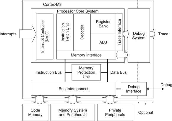
The Cortex-M3 is a 32-bit microprocessor. It has a 32-bit data path, a 32-bit register bank, and 32-bit memory interfaces. The processor has a Harvard architecture, which means it has a separate instruction bus and data bus. This allows instructions and data accesses to take place at the same time, and as a result of this the processor performance increases because data accesses do not affect the instruction pipeline. This feature results in multiple bus interfaces on Cortex-M3, each with optimized usage and the ability to be used simultaneously. However, the instruction and data buses share the same memory space (a unified memory system). In other words, you cannot get 8 GB of memory space just because you have separate bus interfaces.
For complex applications that require more memory system features, the Cortex-M3 processor has an optional MPU, and it is possible to use an external cache if it’s required. Both little endian and big endian memory systems are supported.
The Cortex-M3 processor includes a number of fixed internal debugging components. These components provide debugging operation supports and features such as breakpoints and watchpoints. In addition, optional components provide debugging features such as instruction trace and various types of debugging interfaces.
Registers
The Cortex-M3 processor has registers R0 to R15. R13 (the stack pointer) is banked, with only one copy of the R13 visible at a time.
R0 to R12: General-Purpose Registers
R0 to R12 are 32-bit general-purpose registers for data operations. Some 16-bit Thumb instructions can only access a subset of these registers (low registers, R0 to R7).
R13: Stack Pointers
The Cortex-M3 contains two stack pointers, R13. They are banked so that only one is visible at a time:
- Main Stack Pointer (MSP): The default stack pointer; used by the OS kernel and exception handlers
- Process Stack Pointer (PSP): Used by user application code
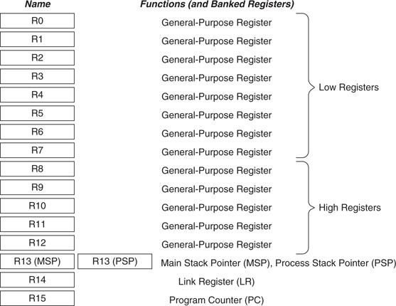
The lowest two bits of the stack pointers are always 0, which means they are always word aligned.
R14: The Link Register
When a subroutine is called, the return address is stored in the link register.
R15: The Program Counter
The program counter is the current program address. This register can be written to control the program flow.
Special Registers
The Cortex-M3 processor also has a number of special registers:
- Program Status Registers (PSRs)
- Interrupt Mask Registers (PRIMASK, FAULTMASK, BASEPRI)
- Control Register (CONTROL)
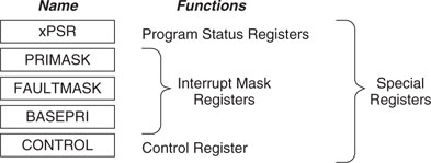
These registers have special functions and can be accessed only by special instructions. They cannot be used for normal data processing.
Table 2.1 Registers and Their Functions
| Register | Function |
| xPSR | Provide ALU flags (zero flag, carry flag), execution status, and current executing interrupt number |
| PRIMASK | Disable all interrupts except the nonmaskable interrupt (NMI) and HardFault |
| FAULTMASK | Disable all interrupts except the NMI |
| BASEPRI | Disable all interrupts of specific priority level or lower priority level |
| CONTROL | Define privileged status and stack pointer selection |
You’ll find more information on these registers in Chapter 3.
Operation Modes
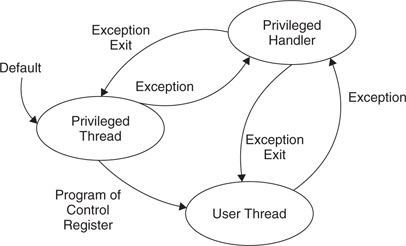
The Cortex-M3 processor has two modes and two privilege levels. The operation modes (thread mode and handler mode) determine whether the processor is running a normal program or running an exception handler like an interrupt handler or system exception handler. The privilege levels (privileged level and user level) provide a mechanism for safeguarding memory accesses to critical regions as well as providing a basic security model.
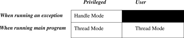
When the processor is running a main program (Thread mode), it can be in either a privileged state or a user state, but exception handlers can only be in a privileged state. When the processor exits reset, it is in Thread mode, with privileged access rights. In the privileged state, a program has access to all memory ranges (except when prohibited by MPU settings) and can use all supported instructions.
Software in the privileged access level can switch the program into the user access level using the control register. When an exception takes place, the processor will always switch back to the privileged state and return to the previous state when exiting the exception handler. A user program cannot change back to the privileged state by writing to the Control register. It has to go through an exception handler that programs the control register to switch the processor back into the privileged access level when returning to Thread mode.
The separation of privilege and user levels improves system reliability by preventing system configuration registers from being accessed or changed by some untrusted programs. If an MPU is available, it can be used in conjunction with privilege levels to protect critical memory locations such as programs and data for operating systems.
For example, with privileged accesses, usually used by the OS kernel, all memory locations can be accessed (unless prohibited by MPU setup). When the OS launches a user application, it is likely to be executed in the user access level to protect the system from failing due to a crash of untrusted user programs.
The Built-In Nested Vectored Interrupt Controller
The Cortex-M3 processor includes an interrupt controller called the Nested Vectored Interrupt Controller (NVIC). It is closely coupled to the processor core and provides a number of features:
- Nested interrupt support
- Vectored interrupt support
- Dynamic priority changes support
- Reduction of interrupt latency
- Interrupt masking
Nested Interrupt Support
The NVIC provides nested interrupt support. All the external interrupts and most of the system exceptions can be programmed to different priority levels. When an interrupt occurs, the NVIC compares the priority of this interrupt to the current running priority level. If the priority of the new interrupt is higher than the current level, the interrupt handler of the new interrupt will override the current running task.
Vectored Interrupt Support
The Cortex-M3 processor has vectored interrupt support. When an interrupt is accepted, the starting address of the interrupt service routine (ISR) is located from a vector table in memory. There is no need to use software to determine and branch to the starting address of the ISR. Thus it takes less time to process the interrupt request.
Dynamic Priority Changes Support
Priority levels of interrupts can be changed by software during run time. Interrupts that are being serviced are blocked from further activation until the interrupt service routine is completed, so their priority can be changed without risk of accidental reentry.
Reduction of Interrupt Latency
The Cortex-M3 processor also includes a number of advanced features to lower the interrupt latency. These include automatic saving and restoring some register contents, reducing delay in switching from one ISR to another (see the discussion of tail chaining interrupts on page 152), and handling late arrival interrupts (see page 153.)
Interrupt Masking
Interrupts and system exceptions can be masked based on their priority level or masked completely using the interrupt masking registers BASEPRI, PRIMASK, and FAULTMASK. They can be used to ensure that time-critical tasks can be finished on time without being interrupted.
The Memory Map
The Cortex-M3 has a predefined memory map. This allows the built-in peripherals, such as the interrupt controller and debug components, to be accessed by simple memory access instructions. Thus most system features are accessible in C program code. The predefined memory map also allows the Cortex-M3 processor to be highly optimized for speed and ease of integration in system-on-a-chip (SoC) designs.
Overall, the 4 GB memory space can be divided into the ranges shown in Figure 2.6.

The Cortex-M3 design has an internal bus infrastructure optimized for this memory usage. In addition, the design allows these regions to be used differently. For example, data memory can still be put into the CODE region, and program code can be executed from an external RAM region.
The system-level memory region contains the interrupt controller and the debug components. These devices have fixed addresses, detailed in Chapter 5 (Memory Systems) of this book. By having fixed addresses for these peripherals, you can port applications between different Cortex-M3 products much more easily.
The Bus Interface
There are several bus interfaces on the Cortex-M3 processor. They allow the Cortex-M3 to carry instruction fetches and data accesses at the same time. The main bus interfaces are:
- Code memory buses
- System bus
- Private peripheral bus
The code memory region access is carried out on the code memory buses, which physically consist of two buses, one called I-Code and another called D-Code. These are optimized for instruction fetches for best instruction execution speed.
The system bus is used to access memory and peripherals. This provides access to the SRAM, peripherals, external RAM, external devices, and part of the system-level memory regions.
The private peripheral bus provides access to a part of the system-level memory dedicated to private peripherals such as debugging components.
The Memory Protection Unit
The Cortex-M3 has an optional Memory Protection Unit, or MPU. This unit allows access rules to be set up for privileged access and user program access. When an access rule is violated, a fault exception is generated, and the fault exception handler will be able to analyze the problem and correct it if possible.
The MPU can be used in various ways. In common scenarios, the MPU is set up by an operating system, allowing data used by privileged code (e.g., the operating system kernel) to be protected from untrusted user programs. The MPU can also be used to make memory regions read-only, to prevent accidental erasing of data, or to isolate memory regions between different tasks in a multitasking system. Overall, it can help make embedded systems more robust and reliable.
The MPU feature is optional and is determined during the implementation stage of the microcontroller or SoC design. For more information on the MPU, refer to Chapter 13.
The Instruction Set
The Cortex-M3 supports the Thumb-2 instruction set. This is one of the most important features of the Cortex-M3 processor because it allows 32-bit instructions and 16-bit instructions to be used together for high code density and high efficiency. It is flexible and powerful yet easy to use.
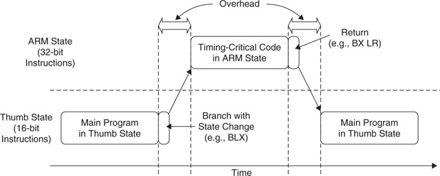
In previous ARM processors, the CPU had two operation states: a 32-bit ARM state and a 16-bit Thumb state. In the ARM state, the instructions are 32-bit and can execute all supported instructions with very high performance. In the Thumb state, the instructions are 16-bit, so there is a much higher instruction code density, but the Thumb state does not have all the functionality of ARM instructions and may require more instructions to complete certain types of operations.
To get the best of both worlds, many applications have mixed ARM and Thumb codes. However, the mixed-code arrangement does not always work best. There is overhead (in terms of both execution time and instruction space) to switch between the states; and ARM code and Thumb code might need to be compiled separately in different files. This increases the complexity of software development and reduces maximum efficiency of the CPU core.
With the introduction of the Thumb-2 instruction set, it is now possible to handle all processing requirements in one operation state. There is no need to switch between the two. In fact, the Cortex-M3 does not support ARM code. Even interrupts are now handled with the Thumb state. (Previously, the ARM core entered interrupt handlers in the ARM state.) Since there is no need to switch between states, the Cortex-M3 processor has a number of advantages over traditional ARM processors:
- No state switching overhead, saving both execution time and instruction space
- No need to separate ARM code and Thumb code source files, making software development and maintenance easier
- It’s easier to get the best efficiency and performance, in turn making it easier to write software, because there is no need to worry about switching code between ARM and Thumb to try to get the best density/performance
The Cortex-M3 processor has a number of interesting and powerful instructions. Here are a few examples:
- UFBX, BFI, BFC: Bit field extract, insert, and clear instructions
- UDIV, SDIV: Unsigned and signed divide instructions
- SEV, WFE, WFI: Send-Event, Wait-For-Event, Wait-For-Interrupts; these allow the processor to handle task synchronization on multiprocessor systems or to enter sleep mode
- MSR, MRS: For access to the special registers
Since the Cortex-M3 processor supports the Thumb-2 instruction set only, existing program code for ARM needs to be ported to the new architecture. Most C applications simply need to be recompiled using new compilers that support the Cortex-M3. Some assembler codes need modification and porting to utilize the new architecture and the new unified assembler framework.
Note that not all the instructions in the Thumb-2 instruction set are implemented on the Cortex-M3. The ARMv7-M Architecture Application Level Reference Manual (Ref 2) only requires a subset of the Thumb-2 instructions to be implemented. For example, coprocessor instructions are not supported on the Cortex-M3 (external data processing engines can be added), and SIMD is not implemented on the Cortex-M3. In addition, a few Thumb instructions are not supported, such as BLX with immediate (used to switch processor state from Thumb to ARM), a couple of CPS instructions, and the SETEND instructions, which were introduced in architecture v6. For a complete list of supported instructions, refer to Appendix A of this book or the Cortex-M3 Technical Reference Manual (Ref 1).
Interrupts and Exceptions
The Cortex-M3 processor implements a new exception model, introduced in the ARMv7-M architecture. This exception model differs from the traditional ARM exception model, enabling very efficient exception handling. It has a number of system exceptions plus a number of external IRQs (external interrupt inputs). There is no FIQ (fast interrupt in ARM7/9/10/11) in the Cortex-M3; however, interrupt priority handling and nested interrupt support are now included in the interrupt architecture. Therefore, it is easy to set up a system that supports nested interrupts (a higher-priority interrupt can override, or preempt, a lower-priority interrupt handler) and that behaves just like the FIQ in traditional ARM processors.
The interrupt features in the Cortex-M3 are implemented in the NVIC. Aside from supporting external interrupts, the Cortex-M3 also supports a number of internal exception sources, such as system fault handling. As a result, the Cortex-M3 has a number of predefined exception types, as shown in Table 2.2.

The number of external interrupt inputs is defined by chip manufacturers. A maximum of 240 external interrupt inputs can be supported. In addition, the Cortex-M3 also has an NMI interrupt input. When it is asserted, the NMI interrupt service routine is executed unconditionally.
Debugging Support
The Cortex-M3 processor includes a number of debugging features such as program execution controls, including halting and stepping, instruction breakpoints, data watchpoints, registers and memory accesses, profiling, and traces.
The debugging hardware of the Cortex-M3 processor is based on the CoreSight architecture. Unlike traditional ARM processors, the CPU core itself does not have a JTAG interface. Instead, a debug interface module is decoupled from the core, and a bus interface called the Debug Access Port (DAP) is provided at the core level. Via this bus interface, external debuggers can access control registers to debug hardware as well as system memory, even when the processor is running. The control of this bus interface is carried out by a Debug Port (DP) device. The DPs currently available are the SWJ-DP (supports the traditional JTAG protocol as well as the Serial Wire protocol) or the SW-DP (supports the Serial Wire protocol only). A JTAG-DP module from the ARM CoreSight product family can also be used. Chip manufacturers can choose to attach one of these DP modules to provide the debug interface.
Chip manufacturers can also include an Embedded Trace Macrocell (ETM) to allow instruction trace. Trace information is output via the Trace Port Interface Unit (TPIU), and the debug host (usually a PC) can then collect the executed instruction information via external trace-capturing hardware.
Within the Cortex-M3 processor, a number of events can be used to trigger debug actions. Debug events can be breakpoints, watchpoints, fault conditions, or external debugging request input signals. When a debug event takes place, the Cortex-M3 can either enter halt mode or execute the debug monitor exception handler.
The data watchpoint function is provided by a Data Watchpoint and Trace (DWT) unit in the Cortex-M3 processor. This can be used to stop the processor (or trigger the debug monitor exception routine) or to generate data trace information. When data trace is used, the traced data can be output via the TPIU. (In the CoreSight architecture, multiple trace devices can share one single trace port.)
In addition to these basic debugging features, the Cortex-M3 processor also provides a Flash Patch and Breakpoint (FPB) unit that can provide a simple breakpoint function or remap an instruction access from Flash to a different location in SRAM.
An Instrumentation Trace Macrocell (ITM) provides a new way for developers to output data to a debugger. By writing data to register memory in the ITM, a debugger can collect the data via a trace interface and display or process it. This method is easy to use and faster than JTAG output.
All these debugging components are controlled via the DAP interface bus on the Cortex-M3 or by a program running on the processor core, and all trace information is accessible from the TPIU.
Characteristics Summary
Why is the Cortex-M3 processor such a revolutionary product? What are the advantages of using the Cortex-M3? The benefits and advantages are summarized in this section.
High Performance
- Many instructions, including multiply, are single cycle. Also, the Cortex-M3 processor outperforms most microcontroller products.
- Separate data and instruction buses allow simultaneous data and instruction accesses to be performed.
- The Thumb-2 instruction set makes state switching overhead history. There’s no need to spend time switching between the ARM state (32-bit) and the Thumb state (16-bit), so instruction cycles and program size are reduced. This feature has also simplified software development, allowing faster time to market and easier code maintenance.
- The Thumb-2 instruction set provides extra flexibility in programming. Many data operations can now be simplified using shorter code. This also means that the Cortex-M3 has higher code density and reduced memory requirements.
- Instruction fetches are 32-bit. Up to two instructions can be fetched in one cycle. As a result, there’s more available bandwidth for data transfer.
- The Cortex-M3 design allows microcontroller products to operate at high clock frequency (over 100 MHz in modern semiconductor manufacturing processes). Even running at the same frequency as most other microcontroller products, the Cortex-M3 has a better clock per instruction (CPI) ratio. This allows more work per MHz, or designs can run at lower clock frequency for lower power consumption.
Advanced Interrupt-Handling Features
- The Built-In Nested Vectored Interrupt Controller (NVIC) supports up to 240 external interrupt inputs. The vectored interrupt feature greatly reduces interrupt latency because there is no need to use software to determine which IRQ handler to serve. In addition, there is no need to have software code to set up nested interrupt support.
- The Cortex-M3 processor automatically pushes registers R0–R3, R12, LR, PSR, and PC in the stack at interrupt entry and pops them back at interrupt exit. This reduces the IRQ handling latency and allows interrupt handlers to be normal C functions (as explained later, in Chapter 8).
- Interrupt arrangement is extremely flexible because the NVIC has programmable interrupt priority control for each interrupt. A minimum of eight levels of priority are supported, and the priority can be changed dynamically.
- Interrupt latency is reduced by special optimization, including late arrival interrupt acceptance and tail-chain interrupt entry.
- Some of the multicycle operations, including Load-Multiple (LDM), Store-Multiple (STM), PUSH, and POP, are now interruptible.
- On receipt of a Nonmaskable Interrupt (NMI) request, immediate execution of the NMI handler is guaranteed unless the system is completely locked up. NMI is very important for many safety-critical applications.
Low Power Consumption
- The Cortex-M3 processor is suitable for low-power designs because of the low gate count.
- It has power-saving mode support (SLEEPING and SLEEPDEEP). The processor can enter sleep mode using Wait for Interrupt (WFI) or Wait for Event (WFE) instructions. The design has separated clocks for essential blocks, so clocking circuits for most parts of the processor can be stopped during sleep.
- The fully static, synchronous, synthesizable design makes the processor easy to be manufactured using any lower power or standard semiconductor process technology.
System Features
- The system provides bit-band operation, byte-invariant big endian mode, and unaligned data access support.
- Advanced fault-handling features include various exception types and fault status registers, making it easier to locate problems.
- With the shadowed stack pointer, stack memory of kernel and user processes can be isolated. With the optional MPU, the processor is more than sufficient to develop robust software and reliable products.
Debug Supports
- Supports JTAG or Serial Wire debug interfaces
- Based on the CoreSight debugging solution; processor status or memory contents can be accessed even when the core is running
- Built-in support for six breakpoints and four watchpoints
- Optional ETM for instruction trace and data trace using DWT
- New debugging features, including fault status registers, new fault exceptions, and Flash patch operations, making debugging much easier
- ITM provides an easy-to-use method to output debug information from test code
- PC Sampler and counters inside the DWT provide code-profiling information