CHAPTER 6 Cortex-M3 Implementation Overview
In This Chapter:
• Bus Interfaces on the Cortex-M3
• Other Interfaces on the Cortex-M3
The Pipeline
The Cortex-M3 processor has a three-stage pipeline. The pipeline stages are instruction fetch, instruction decode, and instruction execution (see Figure 6.1).
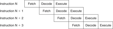
Some people might argue that there are four stages because of the pipeline behavior in the bus interface when it accesses memory, but this stage is outside the processor, so the processor itself still has only three stages.
When running programs with mostly 16-bit instructions, you will find that the processor might not fetch instructions in every cycle. This is because the processor fetches up to two instructions (32-bit) in one go, so after one instruction is fetched, the next one is already inside the processor. In this case, the processor bus interface may try to fetch the instruction after the next or, if the buffer is full, the bus interface could be idle. Some of the instructions take multiple cycles to execute; in this case, the pipeline will be stalled.
In executing a branch instruction, the pipeline will be flushed. The processor will have to fetch instructions from the branch destination to fill up the pipeline again. However, the Cortex-M3 processor supports a number of instructions in v7-M architecture, so some of the short-distance branches can be avoided by replacing them with conditional execution codes.1
Due to the pipeline nature of the processor and to ensure that the program is compatible with Thumb codes, when the program counter is read during instruction execution, the read value will be the address of the instruction plus 4. This offset is constant, independent of the combination of 16-bit Thumb instructions and 32-bit Thumb-2 instructions. This ensures consistency between Thumb and Thumb-2.
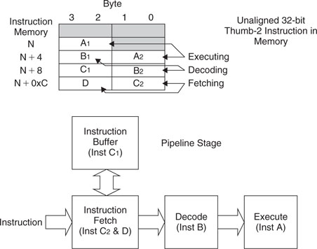
Inside the instruction pre-fetch unit of the processor core, there is also an instruction buffer. This buffer allows additional instructions to be queued before they are needed. This buffer prevents the pipeline being stalled when the instruction sequence contains 32-bit Thumb-2 instructions that are not word aligned. However, this buffer does not add an extra stage to the pipeline, so it does not increase the branch penalty.
A Detailed Block Diagram
The Cortex-M3 processor contains not only the processor core but also a number of components for system management, as well as debugging support components.
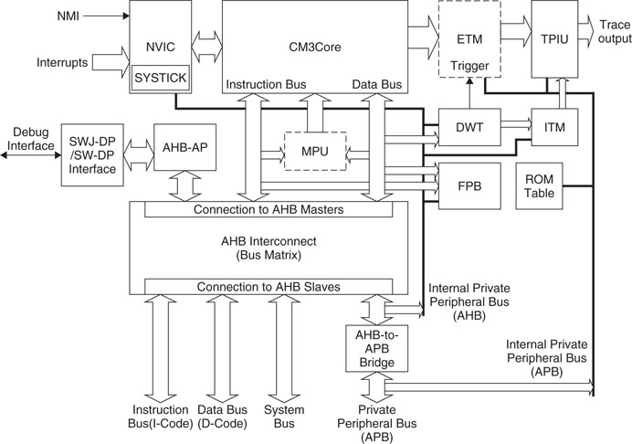
Note that the MPU and ETM blocks are optional blocks that can be included in the microcontroller system at the time of implementation.
A number of new components are shown in this diagram (see Table 6.1).
| Name | Description |
| CM3Core | Central processing core of the Cortex-M3 processor |
| NVIC | Nested Vectored Interrupt Controller |
| SYSTICK Timer | A simple timer that can be used by the operating system |
| MPU | Memory Protection Unit (optional) |
| CM3BusMatrix | Internal AHB interconnection |
| AHB to APB | Bus bridge to convert AHB to APB |
| SW-DP/SWJ-DP interface | Serial Wire/Serial Wire JTAG debug port (DP) interface; debug interface connection implemented using either Serial Wire Protocol or traditional JTAG Protocol (for SWJ-DP) |
| AHB-AP | AHB Access Port; converts commands from Serial Wire/SWJ interface into AHB transfers |
| ETM | Embedded Trace Macrocell; a module to handle instruction trace for debug (optional) |
| DWT | Data Watchpoint and Trace unit; a module to handle the data watchpoint function for debug |
| ITM | Instrumentation Trace Macrocell |
| TPIU | Trace Port Interface Unit; an interface block to send debug data to external trace capture hardware |
| FPB | Flash Patch and Breakpoint unit |
| ROM Table | A small lookup table that stores configuration information |
The Cortex-M3 processor is released as a processor subsystem. The CPU core itself is closely coupled to the interrupt controller (NVIC) and various debug logic blocks:
- CM3Core: The Cortex-M3 core contains the registers, ALU, data path, and bus interface.
- Nested Vectored Interrupt Controller: The NVIC is a built-in interrupt controller. The number of interrupts is customized by chip manufacturers. The NVIC is closely coupled to the CPU core and contains a number of system control registers. It supports nested interrupt handling, which means that with the Cortex-M3, nested interrupt handling is very simple. It also comes with a vectored interrupt feature so that when an interrupt occurs, it can enter the corresponding interrupt handler routine directly, without using a shared handler to determine which interrupt has occurred.
- SYSTICK Timer: The System Tick (SYSTICK) Timer is a basic countdown timer that can be used to generate interrupts at regular time intervals, even when the system is in sleep mode. It makes OS porting between Cortex-M3 devices much easier because there is no need to change the OS’s system timer code. The SYSTICK Timer is implemented as part of the NVIC.
- Memory Protection Unit: The MPU block is optional. This means that some versions of the Cortex-M3 might have the MPU and some might not. If it is included, the MPU can be used to protect memory contents by, for example, making memory regions read-only or preventing user applications from accessing privileged applications data.
- BusMatrix: A BusMatrix is used as the heart of the Cortex-M3 internal bus system. It is an AHB interconnection network, allowing transfer to take place on different buses simultaneously unless both bus masters are trying to access the same memory region. The BusMatrix also provides additional data transfer management, including a write buffer as well as bit-oriented operations (bit-band).
- AHB to APB: An AHB-to-APB bus bridge is used to connect a number of APB devices such as debugging components to the private peripheral bus in the Cortex-M3 processor. In addition, the Cortex-M3 allows chip manufacturers to attach additional APB devices to the external private peripheral bus using this APB bus.
The rest of the components in the block diagram are for debugging support and normally should not be used by application code:
- SW-DP/SWJ-DP: The Serial Wire Debug Port (SW-DP)/Serial Wire JTAG Debug Port (SWJ-DP) work together with the AHB Access Port (AHB-AP) so that external debuggers can generate AHB transfers to control debug activities. There is no JTAG scan chain inside the processor core of the Cortex-M3; most debugging functions are controlled by the NVIC registers through AHB accesses. SWJ-DP supports both the Serial Wire Protocol and the JTAG Protocol, whereas SW-DP can support only the Serial Wire Protocol.
- AHB-AP: The AHB Access Port provides access to the whole Cortex-M3 memory via a few registers. This block is controlled by the SW-DP/SWJ-DP through a generic debug interface called the Debug Access Port (DAP). To carry out debugging functions, the external debugging hardware needs to access the AHB-AP via the SW-DP/SWJ-DP to generate the required AHB transfers.
- Embedded Trace Macrocell: The ETM is an optional component for instruction trace, so some Cortex-M3 products might not have real-time instruction trace capability. Trace information is output to the trace port via TPIU. The ETM control registers are memory mapped, which can be controlled by the debugger via the DAP.
- Data Watchpoint and Trace: The DWT allows data watchpoints to be set up. When a data address or data value match is found, the match hit event can be used to generate watchpoint events to activate the debugger, generate data trace information, or activate the ETM.
- Instrumentation Trace Macrocell: The ITM can be used in several ways. Software can write to this module directly to output information to TPIU, or the DWT matching events can be used to generate data trace packets via ITM for output into a trace data stream.
- Trace Port Interface Unit: The TPIU is used to interface with external trace hardware such as trace port analyzers. Internal to the Cortex-M3, trace information is formatted as Advanced Trace Bus (ATB) packets, and the TPIU reformats the data to allow data to be captured by external devices.
- FPB: The FPB is used to provide Flash Patch and Breakpoint functionalities. Flash Patch means that if an instruction access by the CPU matches a certain address, the address can be remapped to a different location so that a different value is fetched. Alternatively, the matched address can be used to trigger a breakpoint event. The Flash Patch feature is very useful for testing, such as adding diagnosis program code to a device that cannot be used in normal situations unless the FPB is used to change the program control.
- ROM table: A small ROM table is provided. This is simply a small lookup table to provide memory map information for various system devices and debugging components. Debugging systems use this table to locate the memory addresses of debugging components. In most cases, the memory map should be fixed to the standard memory location, as documented in the Cortex-M3 TRM, but because some of the debugging components are optional and additional components can be added, individual chip manufacturers might want to customize their chip’s debugging features. In this case, the ROM table must be customized and used for debugging software to determine the correct memory map and hence detect the type of debugging components available.
Bus Interfaces on the Cortex-M3
Unless you are designing a SoC product using the Cortex-M3 processor, it is unlikely that you can directly access the bus interface signals described here. Normally the chip manufacturer will hook up all the bus signals to memory blocks and peripherals, and in a few cases, you might find that the chip manufacturer connected the bus to a bus bridge and allows external bus systems to be connected off-chip. The bus interfaces on the Cortex-M3 processor are based on AHB-Lite and APB protocols, which are documented in the AMBA Specification (Ref 4).
The I-Code Bus
The I-Code bus is a 32-bit bus based on the AHB-Lite bus protocol for instruction fetches in memory regions from 0x00000000 to 0x1FFFFFFF. Instruction fetches are performed in word size, even for Thumb instructions. Therefore, during execution, the CPU core could fetch up to two Thumb instructions at a time.
The D-Code Bus
The D-Code bus is a 32-bit bus based on the AHB-Lite bus protocol; it is used for data access in memory regions from 0x00000000 to 0x1FFFFFFF. Although the Cortex-M3 processor supports unaligned transfers, you won’t get any unaligned transfer on this bus, because the bus interface on the processor core converts the unaligned transfers into aligned transfers for you. Therefore, devices (such as memory) that attach to this bus need only support AHB-Lite (AMBA 2.0) aligned transfers.
The System Bus
The system bus is a 32-bit bus based on the AHB-Lite bus protocol; it is used for instruction fetch and data access in memory regions from 0x20000000 to 0xDFFFFFFF and 0xE0100000 to 0xFFFFFFFF. As with the to the D-Code bus, all transfers are aligned.
The External Private Peripheral Bus
The External Private Peripheral bus (External PPB) is a 32-bit bus based on the APB bus protocol. This is intended for private peripheral accesses in memory regions 0xE0040000 to 0xE00FFFFF. However, since some part of this APB memory is already used for TPIU, ETM, and the ROM table, the memory region that can be used for attaching extra peripherals on this bus is only 0xE0042000 to 0xE00FF000. Transfers on this bus are word aligned.
The Debug Access Port Bus
The Debug Access Port (DAP) bus interface is a 32-bit bus based on an enhanced version of the APB specification. This is for attaching debug interface blocks such as SWJ-DP or SW-DP. Do not use this bus for other purposes. More information on this interface can be found in Chapter 15, “Debug Architecture,” or in the ARM document CoreSight Technology System Design Guide (Ref 3).
AU2
Other Interfaces on the Cortex-M3
Apart from bus interfaces, the Cortex-M3 processor has a number of other interfaces for various purposes. These signals are unlikely to appear on the pins of the silicon chip, because they are mostly for connecting to various parts of the SoC or are unused. The details of the signals are contained in the Cortex-M3 Technical Reference Manual (TRM) (Ref 1). Table 6.2 contains a short summary of some of them.
Table 6.2 Miscellaneous Interface Signals
| Signal Group | Function |
| Multiprocessor communication (TXEV, RXEV) | Simple task synchronization signals between multiple processors |
| Sleep signals (SLEEPING, SLEEPDEEP) | Sleep status for power management |
| Interrupt status signals (ETMINTNUM, ETMINTSTATE, CURRPRI) | Status of interrupt operation, for ETM operation and debug usage |
| Reset request (SYSRESETREQ) | Resets request output from NVIC |
| Lockup2 and Halted status (LOCKUP, HALTED) | Indicate that the processor core has entered a lockup state (caused by error conditions within hard fault handler or NMI handler) or a halted state (for debug operations) |
| Endian input (ENDIAN) | Sets the endian of the Cortex-M3 when the core is reset |
| ETM interface | Connects to Embedded Trace Macrocell (ETM) for instruction trace |
| ITM’s ATB interface | Advanced Trace Bus (ATB) is a bus protocol in ARM’s CoreSight debug architecture for trace data transfer; here this interface provides trace data output from Cortex-M3’s Instrumentation Trace Macrocell (ITM), which is connected to the Trace Port Interface Unit (TPIU) |
The External Private Peripheral Bus
The Cortex-M3 processor has an External Private Peripheral bus (PPB) interface. The External PPB interface is based on the Advance Peripheral Bus (APB) protocol in AMBA specification 2.0. It is intended for system devices that should not be shared, such as debugging components. To support CoreSight devices, this interface contains an extra signal called PADDR31. This signal indicates the source of a transfer. If this signal is 0, it means that the transfer is generated from software running on the Cortex-M3. If this signal is 1, it means that the transfer is generated by debugging hardware. Based on this signal, a peripheral can be designed so that only a debugger can use it, or when being used by software, only some of the features are allowed.
This bus is not intended for general use, as in peripherals. Although there is nothing to stop chip designers from designing and attaching general peripherals on this bus, users might find it a problem for programming later, due to privileged access-level management—for example, to program the device in the user state or to separate the devices from other memory regions when the MPU is used.
The External PPB does not support unaligned accesses. Since the data width of the bus is 32-bit and APB based, when you’re designing peripherals for this memory region it is necessary to make sure that all register addresses in the peripheral are word aligned. In addition, when writing software accessing devices in this region, it is recommended that you make sure that all the accesses are in word size. The PPB accesses are always in little endian.
Typical Connections
Because there are a number of bus interfaces on the Cortex-M3 processor, you might find it confusing to see how it will connect with other devices such as memory or peripherals. Figure 6.4 shows a simplified example.

Since the Code memory region can be accessed by the instruction bus (if it is an instruction fetch) and from the data bus (if it is a data access), an AHB bus switch called the Bus-Matrix3 or an AHB bus multiplexer is needed. With the Bus-Matrix, the Flash memory and the additional SRAM memory (if implemented) can be accessed by either bus interface. The BusMatrix is available from ARM in the AMBA Development Kit (ADK).4 When both data bus and instruction bus are trying to access the same memory device at the same time, the data bus access could be given higher priority for best performance.
Using the AHB Bus-Matrix, if the instruction bus and the data bus are accessing different memory devices at the same time (for example, an instruction fetch from fetch and a data bus reading data from the additional SRAM), the transfers can be carried out simultaneously. If a bus multiplexer is used, however, the transfers cannot take place at the same time, but the circuit size would be smaller. But common Cortex-M3 microcontroller designs use system bus for SRAM connection.
The main SRAM block should be connected via the system bus interface, using the SRAM memory address region. This allows data access to be carried out at the same time as instruction access. It also allows setting up of Boolean data types by using the bit-band feature.
Some microcontrollers might have an external memory interface. That requires an external memory controller because you cannot connect off chip memory devices directly to AHB. The external memory controller can be connected to the system bus of the Cortex-M3. Additional AHB devices can also be easily connected to the system bus without the need for a Bus-Matrix.
Simple peripherals can be connected to the Cortex-M3 via an AHB-to-APB bridge. This allows the use of the simpler bus protocol APB for peripherals.
The diagram shown in Figure 6.4 is just a very simple example; chip designers might choose different bus connection designs. For software/firmware development, you will only need to know the memory map.
Design blocks shown in the diagram, such as the Bus-Matrix, AHB-to-APB bus bridge, memory controller, I/O interface, timer, and UART, are all available from ARM and a number of IP providers. Since microcontrollers can have different providers for the peripherals, you need to access your microcontroller’s datasheet for the correct programmer model when you’re developing software for Cortex-M3 systems.
Reset Signals
The design of reset circuitry on the Cortex-M3 microcontroller or SoC is implementation specific. In the Cortex-M3 Technical Reference Manual (Ref 1), several reset signals are documented. However, the implemented Cortex-M3 chips will likely have only one or two reset signals, and the rest will be internally generated by reset generators designed by chip vendors. (Refer to the manufacturer datasheet for instructions on how to correctly reset their Cortex-M3-based microcontrollers.) At the Cortex-M3 processor level, you can find the reset signals shown in Table 6.3.
Table 6.3 Various Reset Types on Cortex-M3
| Reset Signal | Description |
| Power on reset (PORESETn) | Reset that should be asserted when the device is powered up; resets both processor core and debugging system |
| System reset (SYSRESETn) | System reset; affects processor core, NVIC (except debug control registers), and MPU but not the debugging system |
| Test reset (nTRST) | Reset for debugging system |

Figure 6.5 Reset Generation of Additional Internal Reset Signals in a Typical Cortex-M3 Microcontroller
1For more information, refer to the “IF-THEN Instructions” section of Chapter 4.
2More information on lockup is included in Chapter 12.
3The Bus-Matrix required here is different from the internal BusMatrix inside the Cortex-M3. The Cortex-M3 internal bus-matrix is specially designed and cannot be used as a general AHB switch.
4ADK is a collection of AMBA components and example systems in VHDL/Verilog.