
CHAPTER 7 Exceptions
In This Chapter:
Exception Types
The Cortex-M3 provides a feature-packed exception architecture that supports a number of system exceptions and external interrupts. Exceptions are numbered 1 to 15 for system exceptions and 16 and above for external interrupt inputs. Most of the exceptions have programmable priority, and a few have fixed priority.
Cortex-M3 chips can have different numbers of external interrupt inputs (from 1 to 240) and different numbers of priority levels. This is because chip designers can configure the Cortex-M3 design source code for different needs.
Exception types 1 to 15 are system exceptions (there is no exception type 0), as outlined in Table 7.1. Exceptions of type 16 or above are external interrupt inputs (see Table 7.2).

Table 7.2 List of External Interrupts
| Exception Number | Exception Type | Priority |
| 16 | External Interrupt #0 | Programmable |
| 17 | External Interrupt #1 | Programmable |
| … | … | … |
| 255 | External Interrupt #239 | Programmable |
The value of the current running exception is indicated by the special register IPSR or from the NVIC’s Interrupt Control State Register (the VECTACTIVE field).
Note that here the interrupt number (e.g., Interrupt #0) refers to the interrupt inputs to the Cortex-M3 NVIC. In actual microcontroller products or SoCs, the external interrupt input pin number might not match the interrupt input number on the NVIC. For example, some of the first few interrupt inputs might be assigned to internal peripherals, and external interrupt pins could be assigned to the next couple of interrupt inputs. Therefore, you need to check the chip manufacturer’s datasheets to determine the numbering of the interrupts.
When an enabled exception occurs but cannot be carried out immediately (for instance, if a higher-priority interrupt service routine is running or if the interrupt mask register is set), it will be pended (except for some fault exceptions1). This means that a register (pending status) will hold the exception request until the exception can be carried out. This is different from traditional ARM processors. Previously, the devices that generate interrupts (such as IRQ/FIQ) must hold the request until they are served. Now, with the pending registers in the NVIC, an occurred interrupt will be handled even if the source requesting the interrupt de-asserts its request signal.
Definitions of Priority
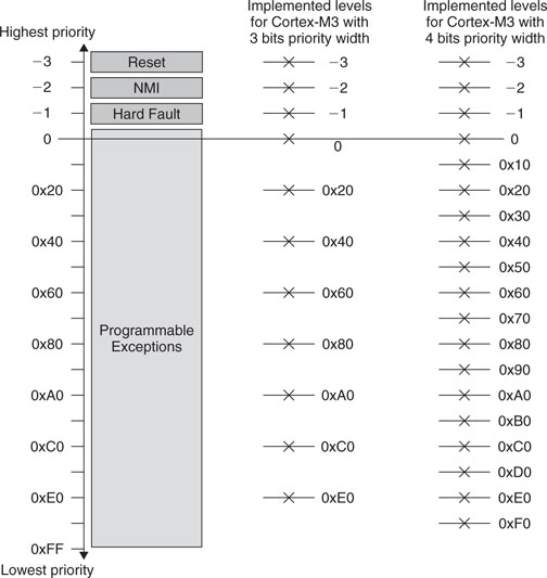
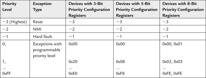
In the Cortex-M3, whether and when an exception can be carried out can be affected by the priority of the exception. A higher-priority (smaller number in priority level) exception can preempt a lower-priority (larger number in priority level) exception; this is the nested exception/interrupt scenario. Some of the exceptions (reset, NMI, and hard fault) have fixed priority levels. They are negative numbers to indicate that they are higher priority than other exceptions. Other exceptions have programmable priority levels.
The Cortex-M3 supports three fixed highest-priority levels and up to 256 levels of programmable priority (a maximum of 128 levels of preemption). However, most Cortex-M3 chips have fewer supported levels—for example, 8, 16, 32, and so on. When a Cortex-M3 chip or SoC is being designed, designers can customize it to obtain the number of levels required. This reduction of levels is implemented by cutting out the LSB part of the priority configuration registers.
For example, if only 3 bits of priority level are implemented in the design, a priority-level configuration register will look like Figure 7.1.
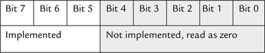
Since bit 4 to bit 0 are not implemented, they are always read as zero, and writes to these bits will be ignored. With this setup, we have possible priority levels of 0x00 (high priority), 0x20, 0x40, 0x60, 0x80, 0xA0, 0xC0, and 0xE0 (the lowest).
Similarly, if 4 bits of priority level are implemented in the design, a priority-level configuration register will look like Figure 7.2.

If more bits are implemented, more priority levels will be available. However, more priority bits can also increase gate counts and hence power consumption. For the Cortex-M3, the minimum number of implemented priority register widths is 3 bits (eight levels).
The reason for removing the LSB of the register instead of the MSB is to make it easier to port software from one Cortex-M3 device to another. In this way, a program written for devices with 4-bit priority configuration registers is likely to be able to run on devices with 3-bit priority configuration registers. If the MSB is removed instead of the LSB, you might get an inversion of priority arrangement when porting an application from one Cortex-M3 chip to another. For example, if an application uses priority level 0x05 for IRQ#0 and level 0x03 for IRQ#1, IRQ#1 should have higher priority. But when MSB bit 2 is removed, IRQ#0 will become level 0x01 and have a higher priority than IRQ#1.
Examples of available exception priority levels for devices with 3-bit, 5-bit, and 8-bit priority registers are shown in Table 7.3.
Table 7.3 Available Priority Levels for Devices with 3-bit, 5-bit, and 8-bit Priority Level Registers
Some readers might wonder, if the priority level configuration registers are 8 bits wide, why there are only 128 preemption levels? This is because the 8-bit register is further divided into two parts: preempt priority and subpriority.
Using a configuration register in the NVIC called Priority Group (a part of the Application Interrupt and Reset Control register in the NVIC, see Table 7.5), the priority-level configuration registers for each exception with programmable priority levels is divided into two halves. The upper half (left bits) is the preempt priority, and the lower half (right bits) is the subpriority (see Table 7.4).
Table 7.4 Definition of Preempt Priority Field and Subpriority Field in a Priority Level Register in Different Priority Group Settings
| Priority Group | Preempt Priority Field | Subpriority Field |
| 0 | Bit [7:1] | Bit [0] |
| 1 | Bit [7:2] | Bit [1:0] |
| 2 | Bit [7:3] | Bit [2:0] |
| 3 | Bit [7:4] | Bit [3:0] |
| 4 | Bit [7:5] | Bit [4:0] |
| 5 | Bit [7:6] | Bit [5:0] |
| 6 | Bit [7] | Bit [6:0] |
| 7 | None | Bit [7:0] |

The preempt priority level defines whether an interrupt can take place when the processor is already running another interrupt handler. The subpriority level value is used only when two exceptions with same preempt priority level occur at the same time. In this case, the exception with higher subpriority (lower value) will be handled first.
As a result of the priority grouping, the maximum width of preempt priority is 7, so there can be 128 levels. When the priority group is set to 7, all exceptions with a programmable priority level will be in the same level, and no preemption between these exceptions will take place, except that hard fault, NMI, and reset, which have priority of –1, –2, and –3, respectively, can preempt these exceptions.
When deciding the effective preempt priority level and subpriority level, you must take these factors into account:
- Implemented priority-level configuration registers
- Priority group setting
For example, if the width of the configuration registers is 3 (bit 7 to bit 5 are available) and priority group is set to 5, you can have four levels of preempt priority levels (bit 7 to bit 6), and inside each preempt level there are two levels of subpriority (bit 5).
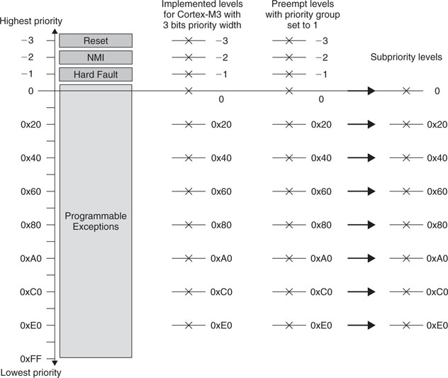
With the setting as shown in Figure 7.4, the available priority levels are illustrated in Figure 7.5. For the same design, if the priority group is set to 0x1, there can be only eight preempt priority levels and no further subpriority levels inside each preempt level. (Bit[1:0] of preempt priority is always 0.) The definition of the priority level configuration registers is shown in Figure 7.6, and the available priority levels are illustrated in Figure 7.7.
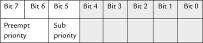
Figure 7.4 Definition of Priority Fields in a 3-bit Priority Level Register with Priority Group Set to 5

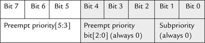
Figure 7.6 Definition of Priority Fields in an 8-bit Priority Level Register with Priority Group Set to 1
If a Cortex-M3 device has implemented all 8 bits in the priority-level configuration registers, the maximum number of preemption levels it can have is only 128, using a priority group setting of 0. The priority fields definition is shown in Figure 7.8.
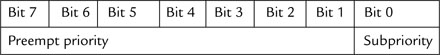
Figure 7.8 Definition of Priority Fields in an 8-bit Priority Level Register with Priority Group Set to 0
When two interrupts are asserted at the same time with exactly the same preempt priority level as well as subpriority level, the interrupt with the smaller exception number has higher priority. (IRQ #0 has higher priority than IRQ #1.)
To avoid unexpected changes of priority levels for interrupts, be careful when writing to the Application Interrupt and Reset Control register (address 0xE000ED0C). In most cases, after the priority group is configured, there is no need to use this register except to generate a reset (see Table 7.5).
Vector Tables
When an exception takes place and is being handled by the Cortex-M3, the processor will need to locate the starting address of the exception handler. This information is stored in the vector table. By default, the vector table starts at address zero, and the vector address is arranged according to the exception number times 4 (see Table 7.6).
Table 7.6 Exception Vector Table After Power Up
| Address | Exception Number | Value (Word Size) |
| 0x00000000 | - | MSP initial value |
| 0x00000004 | 1 | Reset vector (program counter initial value) |
| 0x00000008 | 2 | NMI handler starting address |
| 0x0000000C | 3 | Hard fault handler starting address |
| … | … | Other handler starting address |
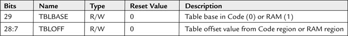
Since the address 0x0 should be boot code, usually it will either be Flash memory or ROM devices, and the value cannot be changed at run time. However, the vector table can be relocated to other memory locations in the Code or RAM region where the RAM is so that we can change the handlers during run time. This is done by setting a register in the NVIC called the vector table offset register (address 0xE000ED08). The address offset should be aligned to the vector table size, extended to the power of 2. For example, if there are 32 IRQ inputs, the total number of exceptions will be 32 + 16 (system exceptions) = 48. Extending it to the power of 2 makes it 64. Multiplying it by 4 makes it 256 (0x100). Therefore, the vector table offset can be programmed as 0x0, 0x100, 0x200, and so on. The vector table offset register contains the items shown in Table 7.7.
In applications where you want to allow dynamic changing of exception handlers, in the beginning of the boot image you need to have these (at a minimum):
These are required because the NMI and hard fault can potentially occur during your boot process. Other exceptions cannot take place until they are enabled.
When the booting process is done, you can define a part of your SRAM as the new vector table and relocate the vector table to the new one, which is writable.
Interrupt Inputs and Pending Behavior
This section describes the behavior of IRQ inputs and pending behavior. It also applies to NMI input, except that an NMI will be executed immediately in most cases, unless the core is already executing an NMI handler, halted by a debugger, or locked up due to some serious system error.
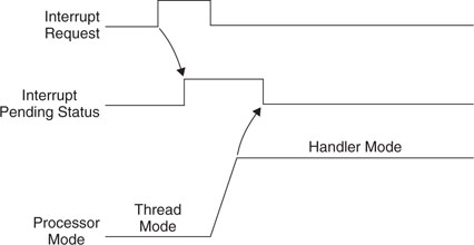
When an interrupt input is asserted, it will be pended. Even if the interrupt source de-asserts the interrupt, the pended interrupt status will still cause the interrupt handler to be executed when the priority is allowed.
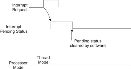
However, if the pending status is cleared before the processor starts responding to the pended interrupt (for example, because pending status register is cleared while PRIMASK/FAULTMASK is set to 1), the interrupt can be canceled (Figure 7.9). The pending status of the interrupt can be accessed in the NVIC and is writable, so you can clear a pending interrupt or use software to pend a new interrupt by setting the pending register.
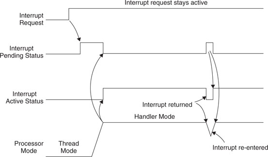
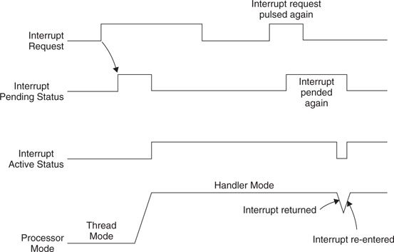
When the processor starts to execute an interrupt, the interrupt becomes active and the pending bit will be cleared automatically (Figure 7.10). When an interrupt is active, you cannot start processing the same interrupt again until the interrupt service routine is terminated with an interrupt return (also called an exception exit, as discussed in Chapter 9). Then the active status is cleared and the interrupt can be processed again if the pending status is 1. It is possible to re-pend an interrupt before the end of the interrupt service routine.

If an interrupt source continues to hold the interrupt request signal active, the interrupt will be pended again at the end of the interrupt service routine as shown in Figure 7.11. This is just like the traditional ARM7TDMI.
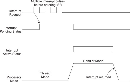
If an interrupt is pulsed several times before the processor starts processing it, it will be treated as one single interrupt request as illustrated in Figure 7.12.
If an interrupt is de-asserted and then pulsed again during the interrupt service routine, it will be pended again as shown in Figure 7.13.
Pending of an interrupt can happen even if the interrupt is disabled; the pended interrupt can then trigger the interrupt sequence when the enable is set later. As a result, before enabling an interrupt, it could be useful to check whether the pending register has been set. The interrupt source might have been activated previously and have set the pending status. If necessary, you can clear the pending status before you enable an interrupt.
Fault Exceptions
A number of system exceptions are useful for fault handling. There are several categories of faults:
- Bus faults
- Memory management faults
- Usage faults
- Hard faults
Bus Faults
Bus faults are produced when an error response is received during a transfer on the AHB interfaces. It can happen at these stages:
- Instruction fetch, commonly called prefetch abort
- Data read/write, commonly called data abort
In the Cortex-M3, bus faults can also occur during a:
- Stack PUSH in the beginning of interrupt processing, called a stacking error
- Stack POP at the end of interrupt processing, called an unstacking error
- Reading of an interrupt vector address (vector fetch) when the processor starts the interrupt-handling sequence (a special case classified as a hard fault)
What Can Cause AHB Error Responses?
Bus faults occur when an error response is received on the AHB bus. The common causes are as follows:
- Attempts to access an invalid memory region (for example, a memory location with no memory attached)
- Device is not ready to accept a transfer (for example, trying to access SDRAM without initializing the SDRAM controller)
- Trying to carry out a transfer with a transfer size not supported by the target device (for example, doing a byte access to a peripheral register that must be accessed as a word)
- The device does not accept the transfer for various reasons (for example, a peripheral that can only be programmed at the privileged access level)
When these types of bus faults (except vector fetches) take place, and if the bus fault handler is enabled and no other exceptions with the same or higher priority are running, the bus fault handler will be executed. If the bus fault handler is enabled but at the same time the core receives another exception handler with higher priority, the bus fault exception will be pending. Finally, if the bus fault handler is not enabled or when the bus fault happens in an exception handler that has the same or higher priority than the bus fault handler, the hard fault handler will be executed instead. If another bus fault takes place when running the hard fault handler, the core will enter a lockup state.2
To enable the bus fault handler, you need to set the BUSFAULTENA bit in the System Handler Control and State register in the NVIC. Before doing that, make sure that the bus fault handler starting address is set up in the vector table if the vector table has been relocated to RAM.
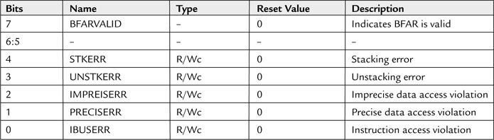
So, how do you find out what went wrong when the processor entered the bus fault handler? The NVIC has a number of fault status registers. One of them is the Bus Fault Status Register (BFSR). From this register the bus fault handler can find out if the fault was caused by data/instruction access or an interrupt stacking or unstacking operation.
For precise bus faults, the offending instruction can be located by the stacked program counter, and if the BFARVALID bit in BFSR is set, it is also possible to determine the memory location that caused the bus fault. This is done by reading another NVIC register called the Bus Fault Address Register (BFAR). However, the same information is not available for imprecise bus faults because by the time the processor receives the error, the processor could have already executed a number of other instructions.
Precise and Imprecise Bus Faults
Bus faults caused by data accesses can be further classified as precise or imprecise. In imprecise bus faults, the fault is caused by an already completed operation (such as a buffered write) that might have occurred a number of clock cycles ago. Precise bus faults are caused by the last completed operation—for example, a memory read is precise on the Cortex-M3 because the instruction cannot be completed until it receives the data.
The programmer’s model for BFSR is as follows: It is 8 bits wide and can be accessed via byte transfer or with a word transfer to address 0xE000ED28 with BFSR in the second byte (see Table 7.8). The error indication bit is cleared when a 1 is written to it.
Memory Management Faults
Memory management faults can be caused by memory accesses that violate the setup in the MPU or by certain illegal accesses (for example, trying to execute code from nonexecutable memory regions), which can trigger the fault, even if no MPU is presented.
Some of the common MPU faults include these:
- Access to memory regions not defined in MPU setup
- Writing to read-only regions
- An access in the user state to a region defined as privileged access only
When a memory management fault occurs, and if the memory management handler is enabled, the memory management fault handler will be executed. If the fault occurs at the same time a higher-priority exception takes place, the other exceptions will be handled first and the memory management fault will be pended. If the processor is already running an exception handler with same or higher priority or if the memory management fault handler is not enabled, the hard fault handler will be executed instead. If a memory management fault takes place inside the hard fault handler or the NMI handler, the processor will enter the lockup state.
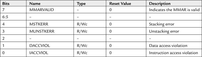
Like the bus fault handler, the memory management fault handler needs to be enabled. This is done by the MEMFAULTENA bit in the System Handler Control and State register in the NVIC. If the vector table has been relocated to RAM, the memory management fault handler starting address should be set up in the vector table first.
The NVIC contains a Memory Management Fault Status Register (MFSR) to indicate the cause of the memory management fault. If the status register indicates that the fault is a data access violation (DACCVIOL bit) or an instruction access violation (IACCVIOL bit), the offending code can be located by the stacked program counter. If the MMARVALID bit in the MFSR is set, it is also possible to determine the memory address location that caused the fault from the Memory Management Address Register (MMAR) in the NVIC.
The programmer’s model for the MFSR is shown in Table 7.9. It is 8 bits wide and can be accessed via byte transfer or with a word transfer to address 0xE000ED28, with the MFSR in the lowest byte. As with other fault status registers, the fault status bit can be cleared by writing 1 to the bit.
Usage Faults
Usage faults can be caused by a number of things:
- Undefined instructions
- Coprocessor instructions (the Cortex-M3 processor does not support a coprocessor, but it is possible to use the fault exception mechanism to run software compiled for other Cortex processors via coprocessor emulation)
- Trying to switch to the ARM state (software can use this faulting mechanism to test whether the processor it is running on supports ARM code; since the Cortex-M3 does not support the ARM state, a usage fault takes place if there’s an attempt to switch)
- Invalid interrupt return (Link Register contains invalid/incorrect values)
- Unaligned memory accesses using multiple load or store instructions
It is also possible, by setting up certain control bits in the NVIC, to generate usage faults for:
- Divide by zero
- Any unaligned memory accesses
When a usage fault occurs and if the usage fault handler is enabled, normally the usage fault handler will be executed. However, if at the same time a higher-priority exception takes place, the usage fault will be pended. If the processor is already running an exception handler with the same or higher priority or if the usage fault handler is not enabled, the hard fault handler will be executed instead. If a usage fault takes place inside the hard fault handler or the NMI handler, the processor will enter the lockup state.
The usage fault handler is enabled by setting the USGFAULTENA bit in the System Handler Control and State register in the NVIC. If the vector table has been relocated to RAM, the usage fault handler starting address should be set up in the vector table first.
The NVIC provides a Usage Fault Status Register (UFSR) for the usage fault handler to determine the cause of the fault. Inside the handler, the program code that causes the error can also be located using the stacked program counter value.
Accidentally Switching to the ARM State
One of the most common causes of usage faults is accidentally trying to switch the processor to ARM mode. This can happen if you load a new value to PC with the LSB equal to 0—for example, if you try to branch to an address in a register (BX LR) without setting the LSB, have zero in the LSB of a vector in the exception vector table, or the stacked PC value to be read by POP {PC} is modified manually, leaving the LSB cleared. When these situations happen, the usage fault exception will take place with the INVSTATE bit in the UFSR set.
The UFSR is shown in Table 7.10. It occupies 2 bytes and can be accessed by half word transfer or as a word transfer to address 0xE000ED28 with the UFSR in the upper half word. As with other fault status registers, the fault status bit can be cleared by writing 1 to the bit.

Hard Faults
The hard fault handler can be caused by usage faults, bus faults, and memory management faults if their handler cannot be executed. In addition, it can also be caused by a bus fault during vector fetch (reading of a vector table during exception handling). In the NVIC there is a hard fault status register that can be used to determine whether the fault was caused by a vector fetch. If not, the hard fault handler will need to check the other fault status registers to determine the cause of the hard fault.
Details of the Hard Fault Status Register (HFSR) are shown in Table 7.11. As with other fault status registers, the fault status bit can be cleared by writing 1 to the bit.

Dealing with Faults
During software development, we can use the Fault Status Registers (FSRs) to determine the causes of errors in the program and correct them. A troubleshooting guide is included in Appendix E of this book for common causes of various faults. In a real running system, the situation is different. After the cause of a fault is determined, the software will have to decide what to do next. In systems that run an OS, the offending tasks or applications could be terminated. In some other cases, the system might need a reset. The requirements of fault recovery depend on the target application. Doing it properly could make the product more robust, but it is best to prevent the faults from happening in the first place. Here are some fault-handling methods:
- Reset: This can be carried out using the VECTRESET control bit in the Application Interrupt and Reset Control register in the NVIC. This will reset the processor but not the whole chip. Depending on the chip’s reset design, some Cortex-M3 chips can be reset using the SYSRESETREQ in the same register. This could provide a full system reset.
- Recovery: In some cases it might be possible to resolve the problem that caused the fault exception. For example, in the case of coprocessor instructions, the problem can be resolved using coprocessor emulation software.
- Task termination: For systems running an OS, it is likely that the task that caused the fault will be terminated and restarted if needed.
The FSRs retain their status until they are cleared manually. Fault handlers should clear the fault status bit they have dealt with. Otherwise, the next time another fault takes place, the fault handler will be invoked again and could mistake that the first fault still exists and so will try to deal with it again. The FSRs use a write-to-clear mechanism (clear by writing 1 to the bits that need to be cleared).
Chip manufacturers can also include an auxiliary FSR in the chip to indicate other fault situations. The implementation of an AFSR depends on individual chip design requirements.
SVC and PendSV
SVC (System Service Call) and PendSV (Pended System Call) are two exceptions targeted at software and operating systems. SVC is for generating system function calls. For example, instead of allowing user programs to directly access hardware, an operating system may provide access to hardware via an SVC. So when a user program wants to use certain hardware, it generates the SVC exception using SVC instructions, and then the software exception handler in the operating system is executed and provides the service the user application requested. In this way, access to hardware is under the control of the OS, which can provide a more robust system by preventing the user applications from directly accessing hardware.
SVC can also make software more portable because the user application does not need to know the programming details of the hardware. The user program will only need to know the Application Programming Interface (API) function ID and parameters; the actual hardware-level programming is handled by device drivers.

SVC is generated using the SVC instruction. An immediate value is required for this instruction, which works as a parameter-passing method. The SVC exception handler can then extract the parameter and determine what action it needs to perform. For example:
![]()
When the SVC handler is executed, you can determine the immediate data value in the SVC instruction by reading the stacked Program Counter value, then reading the instruction from that address and masking out the unneeded bits. If the system uses a PSP for user applications, you might need to determine which stack was used first. This can be determined from the link register value when the handler is entered. (This topic is covered in more depth in Chapter 8).
SVC and SWI (ARM7)
If you have used traditional ARM processors (such as the ARM7), you might know that they have a software interrupt instruction (SWI). The SVC has a similar function, and in fact the binary encoding of SVC instructions is the same as SWI in ARM7. However, since the exception model has changed, this instruction is renamed to make sure that programmers will properly port software code from ARM7 to the Cortex-M3.
Due to the interrupt priority model in the Cortex-M3, you cannot use SVC inside an SVC handler (because the priority is the same as the current priority). Doing so will result in a usage fault. For the same reason, you cannot use SVC in an NMI handler or a hard fault handler.
PendSV (Pended System Call) works with SVC in the OS. Although SVC (by SVC instruction) cannot be pended (an application calling SVC will expect the required task to be done immediately), PendSV can be pended and is useful for an OS to pend an exception so that an action can be performed after other important tasks are completed. PendSV is generated by writing 1 to the NVIC PendSV pending register.
A typical use of PendSV is context switching (switching between tasks). For example, a system might have two active tasks, and context switching can be triggered by:
- Calling an SVC function
- The system timer (SYSTICK)
Let’s look at a simple example of having only two tasks in a system, and a context switch is triggered by SYSTICK exceptions (see Figure 7.15).
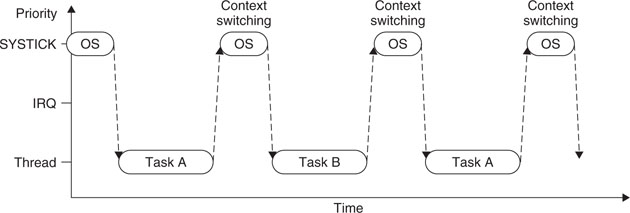
If an interrupt request takes place before the SYSTICK exception, the SYSTICK exception will preempt the IRQ handler. In this case, the OS should not carry out the context switching. Otherwise the IRQ handler process will be delayed, and for the Cortex-M3, a usage fault could be generated if the OS tries to switch to Thread mode when an interrupt is active.
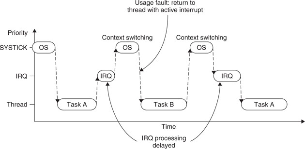
To avoid the problem of delaying the IRQ processing, some OS implementations carry out only context switching if they detect that none of the IRQ handlers are being executed. However, this can result in a very long delay for task switching, especially if the frequency of an interrupt source is close to that of the SYSTICK exception.
The PendSV exception solves the problem by delaying the context-switching request until all other IRQ handlers have completed their processing. To do this, the PendSV is programmed as the lowest priority exception. If the OS detects that an IRQ is currently active (IRQ handler running and preempted by SYSTICK), it defers the context switching by pending the PendSV exception.
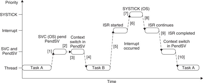
- Task A calls SVC for task switching (for example, waiting for some work to complete).
- The OS receives the request, prepares for context switching, and pends the PendSV exception.
- When the CPU exits SVC, it enters PendSV immediately and does the context switch.
- When PendSV finishes and returns to Thread level, it executes Task B.
- An interrupt occurs and the interrupt handler is entered.
- While running the interrupt handler routine, a SYSTICK exception (for OS tick) takes place.
- The OS carries out the essential operation, then pends the PendSV exception and gets ready for the context switch.
- When the SYSTICK exception exits, it returns to the interrupt service routine.
- When the interrupt service routine completes, the PendSV starts and does the actual context switch operations.
- When PendSV is complete, the program returns to Thread level; this time it returns to Task A and continues the processing.
1There are a few exceptions for the exception-pending behavior. If a fault takes place and the corresponding fault handler cannot be executed immediately because a higher-priority handler is running, the hard fault handler (highest priority fault handler) might be executed instead. More details on this topic are covered later in this chapter, where we look at fault exceptions; full details can be found in the Cortex-M3 Technical Reference Manual and the ARM v7-M Architecture Application Level Reference Manual.
2More information on the lockup state is covered in Chapter 12.