CHAPTER 13 The Memory Protection Unit
Overview
The Cortex-M3 design includes an optional Memory Protection Unit (MPU). Including the MPU in the microcontrollers or SoC products provides memory protection features, which can make the developed products more robust. The MPU needs to be programmed and enabled before use. If the MPU is not enabled, the memory system behavior is the same as though no MPU is present.
The MPU can improve the reliability of an embedded system by:
- Preventing user applications from corrupting data used by the operating system
- Separating data between processing tasks by blocking tasks from accessing others’ data
- Allowing memory regions to be defined as read-only so that vital data can be protected
- Detecting unexpected memory accesses (for example, stack corruption)
In addition, the MPU can also be used to define memory access characteristics such as caching and buffering behaviors for different regions.
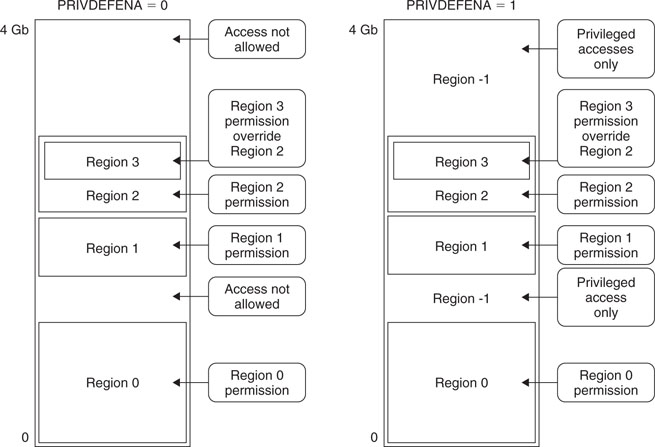
The MPU sets up the protection by defining the memory map as a number of regions. Up to eight regions can be defined, but it is also possible to define a default background memory map for privileged accesses. Accesses to memory locations that are not defined in the MPU regions or not permitted by the region settings will cause the memory management fault exception to take place.
MPU regions can be overlapped. If a memory location falls on two regions, the memory access attributes and permission will be based on the highest-numbered region. For example, if a transfer address is within the address range defined for region 1 and region 4, the region 4 settings will be used.
MPU Registers
The MPU contains a number of registers. The first one is the MPU Type register (see Table 13.1).
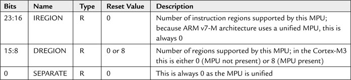
The MPU Type register can be used to determine whether the MPU is fitted. If the DREGION field is read as 0, the MPU is not implemented (see Table 13.2).
By using PRIVDEFENA and if no other regions are set up, privileged programs will be able to access all memory locations, and only user programs will be blocked. However, if other MPU regions are programmed and enabled, they can override the background region. For example, for two systems with similar region setups but only one with PRIVDEFENA set to 1 (the right-hand side in Figure 13.1), the one with PRIVDEFENA set to 1 will allow privileged access to background regions.
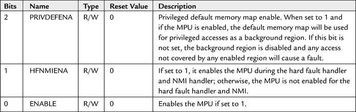
Setting the enable bit in the MPU Control register is usually the last step in the MPU setup code. Otherwise the MPU might generate faults by accident before the region configuration is done. In some situations, it might be worth clearing the MPU Enable at the start of the MPU configuration routine to make sure that the MPU faults won’t be triggered by accident during setup of MPU regions.
Before each region is set up, write to this register to select the region to be programmed (see Table 13.3).
Table 13.3 MPU Region Number Register (0xE000ED98)

Using the VALID and REGION fields in the MPU Region Base Address register (see Table 13.4), we can skip the step of programming the MPU Region Number register. This might reduce the complexity of the program code, especially if the whole MPU setup is defined in a lookup table.
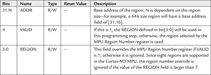
We also need to define the memory address and properties of each region. This is controlled by the MPU Region Base Attribute and Size register (see Table 13.5).
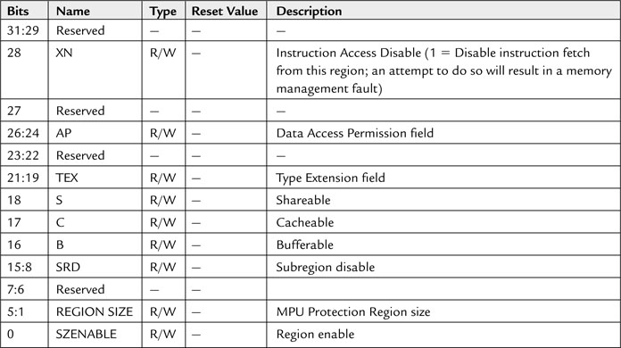
The REGION SIZE field (5-bit) in the MPU Region Base Attribute and Size register determines the size of the region (see Table 13.6).
Table 13.6 Encoding of REGION Field for Different Memory Region Sizes
| REGION Size | Size |
| b00000 | Reserved |
| b00001 | Reserved |
| b00010 | Reserved |
| b00011 | Reserved |
| b00100 | 32 Byte |
| b00101 | 64 Byte |
| b00110 | 128 Byte |
| b00111 | 256 Byte |
| b01000 | 512 Byte |
| b01001 | 1 KB |
| b01010 | 2 KB |
| b01011 | 4 KB |
| b01100 | 8 KB |
| b01101 | 16 KB |
| b01110 | 32 KB |
| b01111 | 64 KB |
| b10000 | 128 KB |
| b10001 | 256 KB |
| b10010 | 512 KB |
| b10011 | 1 MB |
| b10100 | 2 MB |
| b10101 | 4 MB |
| b10110 | 8 MB |
| b10111 | 16 MB |
| b11000 | 32 MB |
| b11001 | 64 MB |
| b11010 | 128 MB |
| b11011 | 256 MB |
| b11100 | 512 MB |
| b11101 | 1 GB |
| b11110 | 2 GB |
| b11111 | 4 GB |
The subregion disable field (bit [15:8] of the MPU Region Base Attribute and Size register) is used to divide a region into eight equally sized subregions and define each of them as enable or disable. If a subregion is disabled and it was overlapped with another region, the access rules for the other region are applied. If the subregion is disabled and it does not overlap any other region, access to this memory range will result in a memory management fault. Subregions cannot be used if the region size is 128 bytes or less.
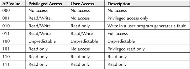
The Data Access Permission (AP) field (bit[26:24]) defines the access permission of the region (see Table 13.7).
The XN (Execute Never) field (bit [28]) decides whether an instruction fetch from this region is allowed. When this field is set to 1, all instructions fetched from this region will generate a memory management fault when they enter the execution stage.
The TEX, S, B, and C fields (bit [21:16]) are more complex. Despite the fact that the Cortex-M3 processor does not have cache, its implementation follows ARM v7-M architecture, which can support external cache and more advanced memory systems. Therefore, the region access properties can be programmed to support different types of memory management models.
In v6 and v7 architecture, the memory system can have two cache levels: inner cache and outer cache. They can have different caching policies. Since the Cortex-M3 processor itself does not have a cache controller, the cache policy only affects write buffering in the internal bus matrix and possibly the memory controller (see Table 13.8).
Table 13.8 [S] Indicates That Shareability Is Determined by the S Bit Field (Shared by Multiple Processors)

When TEX[2] is 1, the cache policy for outer cache and inner cache are as shown in Table 13.9.
Table 13.9 Encoding of Inner and Outer Cache Policy When Most Significant Bit of TEX is Set to 1
| Memory Attribute Encoding (AA and BB) | Cache Policy |
| 00 | Noncacheable |
| 01 | Write back, write and read allocate |
| 10 | Write through, no write allocate |
| 11 | Write back, no write allocate |
For more information on cache behavior and cache policy, refer to the ARM Architecture Application Level Reference Manual (Ref 2).
Setting Up the MPU
The MPU register might look complicated, but as long as you have a clear idea of the memory regions that are required for your application, it should not be difficult. Typically, you will need to have the following memory regions:
- Program code for privileged programs (for example, OS kernel and exception handlers)
- Program code for user programs
- Data memory for privileged programs within Code region (data + stack)
- Data memory for user programs within Code region (data + stack)
- Data memory for privileged and user programs in other memory regions (e.g., SRAM)
- System device region (usually privileged access only; for example, NVIC and MPU registers)
- Other peripherals
For Cortex-M3 products, most memory regions can be set up with TEX = b000, C = 1, B = 1. System devices such as the NVIC should be strongly ordered, and peripheral regions can be programmed as shared devices (TEX=b000, C= 0, B = 1). However, if you want to make sure that any bus faults occurring in the region are precise bus faults, you should use strong ordering (TEX = b000, C = 0, B = 0) so that write buffering is disabled. However, doing so can reduce system performance.
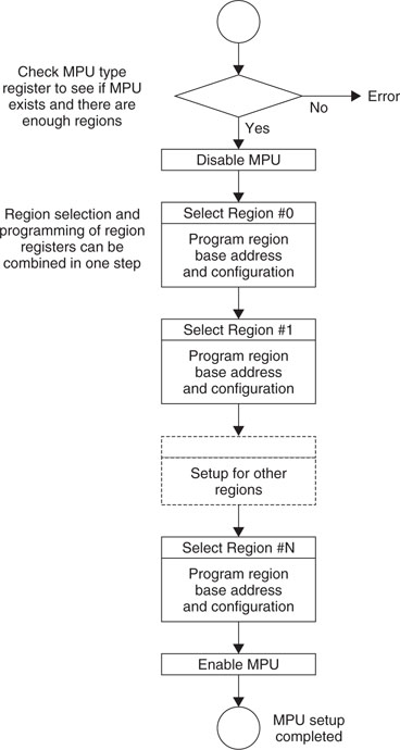
A simple flow for an MPU setup routine might look like the diagram shown in Figure 13.2.
Before the MPU is enabled and if the vector table is relocated to RAM, remember to set up the fault handler for the memory management fault in the vector table, and enable the memory management fault in the System Handler Control and State register. They are needed to allow the memory management fault handler to be executed if an MPU violation takes place.
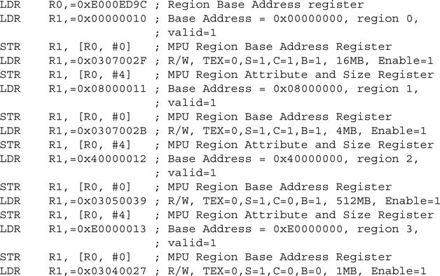
For a simple case of only four required regions, a simple MPU setup code (without the region checking and enabling) might look like this:
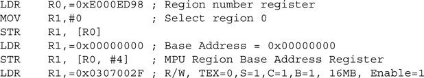
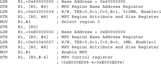
This provides four regions:
- Privileged code: 0x00000000–0x00FFFFFF (16 MB), full access, cacheable
- Privileged data: 0x08000000–0x0803FFFF (4 MB), full access, cacheable
- Peripheral: 0x40000000–0x5FFFFFFF (0.5 GB), full access, shared device
- System control: 0xE0000000–0xE00FFFFF (1 MB), privileged access, strongly ordered, XN
By combining region selection and writing to the base address register, we can shorten the code to this:

We’ve shortened the code quite a bit. However, you can make further enhancements to create even faster setup code. This is done using MPU aliased register addresses (see Table D.33 in Appendix D). The aliased register addresses follow the MPU Region Attribute and Size registers and are aliased to the MPU Base Address register and the MPU Region Attribute and Size register. They produce a continuous address of 8 words, making it possible to use load/store multiple (LDM and STM) instructions:
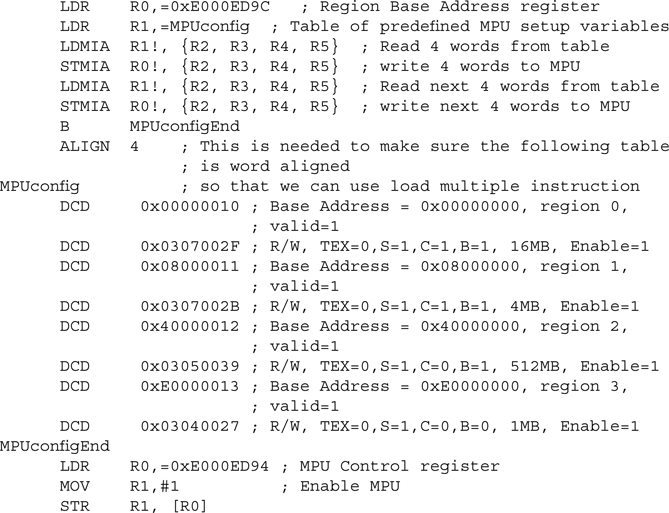
This solution, of course, can be used only if all the required information is known beforehand. Otherwise, a more generic approach has to be used. One way to handle this is to use a subroutine (MpuRegionSetup) that can set up a region based on a number of input parameters and then call it several times to set up different regions:

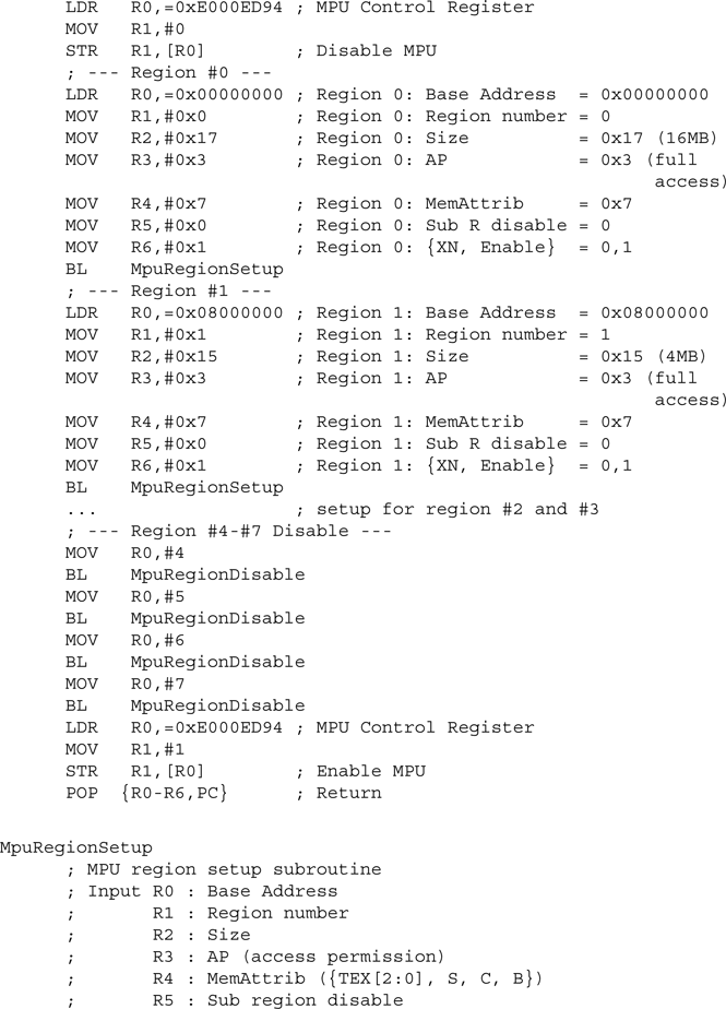

In this example, we included a subroutine that is used to disable a region that is not used. This is necessary if you do not know whether a region has been programmed previously. If an unused region is previously programmed to be enabled, it needs to be disabled so that it doesn’t affect the new configuration.
In addition, the example shows the application of the Bit Field Insert (BFI) instruction in the Cortex-M3. This can greatly simplify bit-field merging operations.
Typical Setup
In typical applications, the MPU is used when there is a need to prevent user programs from accessing privileged process data and program regions. When developing the setup routine for the MPU, you need to consider a number of regions:
- Code region:
- Privileged code, including a starting vector table
- User code
- SRAM region:
- Privileged data, including the main stack
- User data, including the process stack
- Privileged bit-band alias region
- User bit-band alias region
- Peripherals:
- Privileged peripherals
- User peripherals
- Privileged peripheral bit-band alias region
- User peripheral bit-band alias region
- System Control Space (NVIC and debug components):
- Privileged accesses only
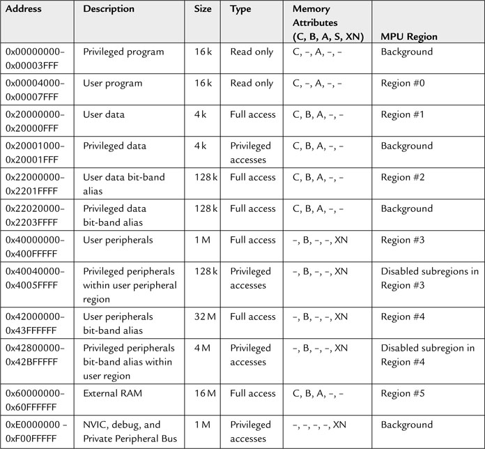
From this list we have identified 11 regions, more than the eight regions supported by the Cortex-M3 MPU. However, we can define the privileged regions by means of a background region (PRIVDEFENA set to 1), so there are only five user regions to set up, leaving three spare MPU regions. The unused regions might still be used for setting up additional regions in external memory, to protect read-only data, or to completely block some part of the memory if necessary.
Example Use of the Subregion Disable
In some cases we might have some peripherals accessible by user programs, and a few should be protected to be privileged accesses only, resulting in fragmentation of user-accessible peripheral memory space. In this kind of scenario, we could do one of these things:
- Define multiple user regions
- Define privileged regions inside the user peripheral region
- Use subregion disable within the user region
The first two methods can use up available regions very easily. With the third solution, using the subregion disable feature, we can easily set up access permission to separate peripheral blocks without using extra regions. For example:
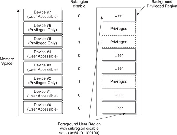
The same techniques can be applied to memory regions as well. However, it is more likely that peripherals will have a fragmented privilege setup.
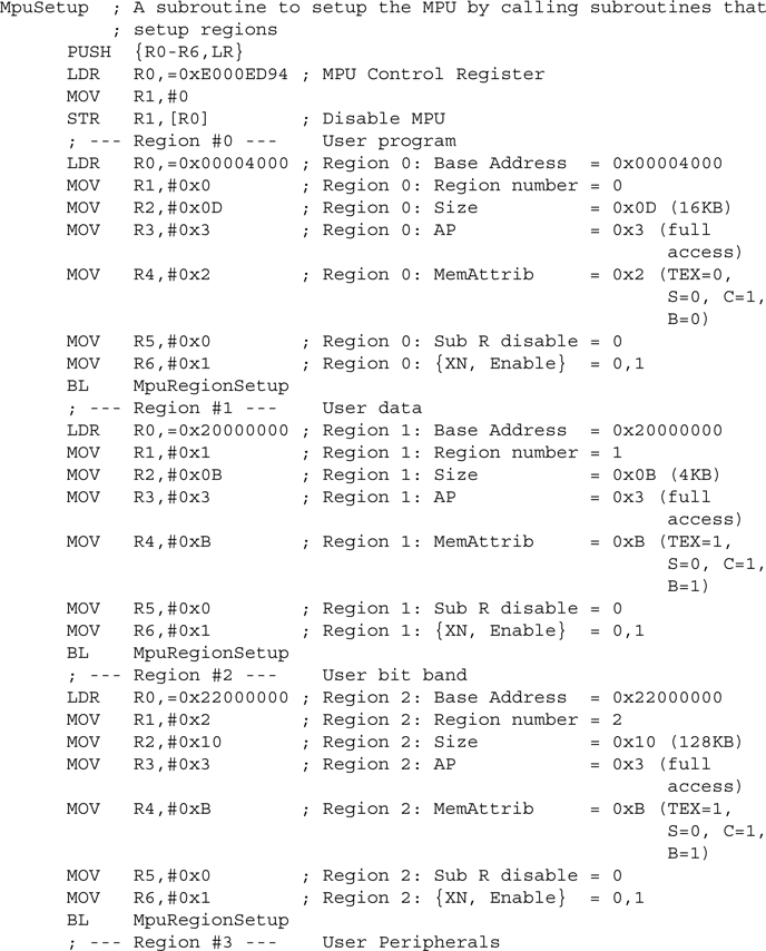
Let’s assume that the memory regions in Table 13.10 will be used. After the required regions are defined, we can create the MPU setup code. To make the code easier to understand and modify, we used the function we created earlier to develop the completed MPU setup example: