Chapter 7. Adding Peripherals Using SPI
Thirty spokes meet at a nave;
Because of the hole we may use the wheel.
Clay is molded into a vessel;
Because of the hollow we may use the cup.
Walls are built around a hearth;
Because of the doors we may use the house.
Thus tools come from what exists,
But use from what does not.
—Lao Tse, Tao Te Ching
In this chapter and the next, we’ll look at two low-cost interfaces used to connect peripheral chips to microcontrollers, within a single embedded system. These interfaces allow you to connect devices such as real-time clocks, nonvolatile memories for parameter storage, sensor interfaces, and much more. The interfaces are easy to use and cheap to implement, making them ideal for small, embedded applications. Some microcontrollers incorporate both types of interface, whereas others may only have one or the other. The one to use really depends on what your processor has to offer and the requirements of the particular peripheral you’re using.
Serial Peripheral Interface
The Serial Peripheral Interface (known as SPI) was developed by Motorola to provide a low-cost and simple interface between microcontrollers and peripheral chips. (SPI is sometimes also known as a four-wire interface.) It can be used to interface to memory (for data storage), analog-digital converters, digital-analog converters, real-time clock calendars, LCD drivers, sensors, audio chips, and even other processors. The range of components that support SPI is large and growing all the time.
Unlike a standard serial port, SPI is a synchronous protocol in which all transmissions are referenced to a common clock, generated by the master (processor). The receiving peripheral (slave) uses the clock to synchronize its acquisition of the serial bit stream. Many chips may be connected to the same SPI interface of a master. A master selects a slave to receive by asserting the slave’s chip select input. A peripheral that is not selected will not take part in a SPI transfer.
SPI uses four main signals:
Master Out Slave In
(MOSI), Master In Slave Out (MISO), Serial CLocK (SCLK or SCK) and Chip Select (![]() ) for the peripheral. Some processors have a dedicated chip select for SPI interfacing called Slave Select (
) for the peripheral. Some processors have a dedicated chip select for SPI interfacing called Slave Select (![]() ).
).
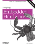
MOSI is generated by the master and is received by the slave. On some chips, MOSI is labeled simply as Serial In (SI) or Serial Data In (SDI). MISO is produced by the slave, but its generation is controlled by the master. MISO is sometimes known as Serial Out (SO) or Serial Data Out (SDO) on some chips. The chip select to the peripheral is normally generated by simply using a spare I/O pin of the master. Figure 7-1 shows a microprocessor interfaced to a peripheral using SPI.
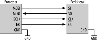
Both masters and slaves contain a serial shift register. The master starts a transfer of a byte by writing it to its SPI shift register. As the register transmits the byte to the slave on the MOSI signal line, the slave transfers the contents of its shift register back to the master on the MISO signal line (Figure 7-2). In this way, the contents of the two shift registers are exchanged. Both a write and a read operation are performed with the slave simultaneously. SPI can therefore be a very efficient protocol.
If only a write operation is desired, the master just ignores the byte it receives. Conversely, if the master just wishes to read a byte from the slave, it must transfer a dummy byte in order to initiate a slave transmission.
Some peripherals can handle multiple byte transfers, where a continuous stream of data is shifted from the master. Many memory chips with SPI interfaces work this way. With this type of transfer, the chip select for the SPI slave must remain low for the entire duration of the transmission. For example, a memory chip might expect a “write” command to be followed by four address bytes (starting address), then the data bytes to be stored. A single transfer may involve the shifting of a kilobyte or more of information.
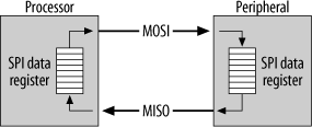
Other slaves need only a single byte (for example, a command byte for an analog-digital converter), and some even support being daisy-chained together (Figure 7-3).
In this example, the master processor transmits three bytes out of its SPI interface. The first byte is shifted into slave A. As the second byte is transferred to slave A, the first byte is shifted out of slave A and into slave B. Similarly, as the third byte is shifted into slave A, the second byte is shifted into slave B, and the first byte is shifted into slave C. If the master wishes to read a result from slave A, it must again transfer a three-byte (dummy) sequence. This will move the byte from slave A into slave B, then into slave C, and finally into the master. In the process, the master also receives bytes from slave C and slave B in turn.
Note that daisy chaining won’t necessarily work with all SPI devices, especially ones that require multibyte transfers (such as memory chips). Again, it’s a case of checking the slave chips’ datasheets carefully to determine what you can and can’t do. If the datasheet doesn’t explicitly mention daisy chaining, then it’s a fair bet the device doesn’t support it.
SPI has four modes of operation, depending on clock polarity and clock phase. For low clock polarity, the clock (SCK) is low when idle and toggles high during a transfer. When configured for high clock polarity, the clock is high when idle and toggles low during a transfer.
The two clock phases are known as clock phase zero and clock phase one. For clock phase zero, MOSI and MISO outputs are valid on the rising edge of the clock (SCK) if the clock polarity is low (Figure 7-4). If the clock polarity is high, these outputs are valid on the falling edge of SCK, for clock phase zero (Figure 7-5). The “X” bit output on MISO is an undefined extra bit and is a consequence of the SPI interface. You don’t need to worry about it, as the SPI interfaces ignore it.
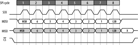
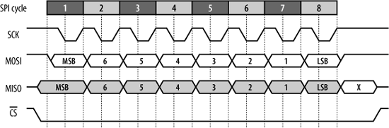
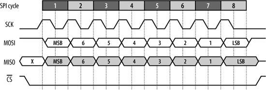
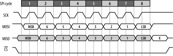
Conversely, for clock phase one, the opposite is true. MOSI and MISO are valid on the falling edge of the clock if clock polarity is low (Figure 7-6). They are valid on the rising edge of the clock if the clock polarity is high (Figure 7-7).
SPI-Based Clock/Calendar
There is a wide variety of SPI devices available, and we’ll be looking at several in the coming chapters. In the meantime, to see how a SPI interface is used to add a peripheral to a microcontroller, let’s look at interfacing a processor to a clock/calendar chip. Such chips contain an oscillator module driven by a crystal, just like a processor. The oscillator module ticks over internal counters that track milliseconds, seconds, minutes, hours, days, months, and years. They are specifically designed to provide accurate timekeeping, and many have additional functions such as an “alarm” (whereby the processor is interrupted at a specific time) and a watchdog. Some also include voltage monitoring, such that the clock chip may act as a system monitor, alerting the processor should the power supply be wavering. There are a number of clock chips available (and not all are interfaced using SPI). For this example, we will use the Maxim DS1305.
The way in which we interface the clock chip to a processor is virtually identical for all other SPI devices. Some chips with SPI interfaces have special requirements, but most are very simple and straightforward. This makes SPI a very useful interface that makes increasing system functionality trivial.
The Maxim DS1305 Real-Time Clock (RTC) provides timekeeping services and tracks seconds, minutes, hours, day of the month, month, day of the week, and year. It knows which months have 30 days and which have 31. It even automatically adjusts for leap years, up to the year 2100. It can generate two interrupts to the microcontroller for time-of-day alarms. These alarms can be used to trigger a regular system event, such as a backup or user notification.
The DS1305 can run off two separate power sources and supports battery backup of its internal state. The chip can use a power supply in the range of 2 V to 5.5 V, allowing it to be powered from a variety of sources. It also has 96 bytes of static RAM, used for parameter storage. You could use the RAM for holding variables indicating system mode, secure password storage, or even authorization codes for your embedded software, just as desktop software does.
Tip
If you are producing commercial embedded systems and have problems with late-paying customers, you can use this RAM to hold a license number. When you ship the system, you design it to work for perhaps 45 days before shutting down. When your customer pays her bill, and you supply her with the right magic number, the system comes back to life again. The system stores the license number in the RAM of the RTC and from then on works as normal.
The RAM, like the timekeeping function, is battery-backed, and so its contents will be retained for the life of the battery. This can be up to 10 years, depending on the battery chosen. Thus, the contents of the internal parameter RAM will probably last for the expected operational lifespan of an embedded system.
The DS1305 is versatile in the way it can be powered. It has three power-supply inputs--VCC1, VCC2, and VBAT--from which it can choose to draw power. VCC1 is the primary supply input and is connected directly to the system’s power supply. When the computer is up and running, the DS1305 draws its current from this source. VCC2 is the secondary power source, and this can be a rechargeable battery. VBAT is the third power source and is for nonrechargeable batteries.
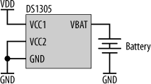
There are three, and only three, possible configurations for powering the DS1305, and it is important for correct operation that the power inputs are appropriately driven. Figure 7-8 shows the DS1305 powered by a primary DC supply connected to VCC1 and a secondary, nonrechargeable battery connected to VBAT. (To keep the diagram simple, only the power pins are shown. We’ll look at the data interface in a moment.) For this configuration, VCC2 is unused and must be connected to GND. When VCC1 falls below a given threshold voltage (the primary power source has failed), the internal memory and registers of the DS1305 become write-protected to prevent them from being corrupted by a failing microprocessor.
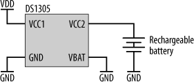
If the secondary power source is a rechargeable battery, then the DS1305 may be wired as shown in Figure 7-9. When using a rechargeable battery on VCC2, VBAT must be connected to GND. When the device is used in this mode, there is no automatic write protection for the DS1305 if VCC1 fails.
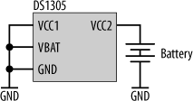
Finally, the DS1305 may be used with only a battery as its primary power source and no backup power supply. This is shown in Figure 7-10. For this configuration, both VCC1 and VBAT are connected to ground, while the battery is connected to VCC2.
Using the DS1305 is very simple. The schematic showing a DS1305 interfaced to a microcontroller is shown in Figure 7-11.
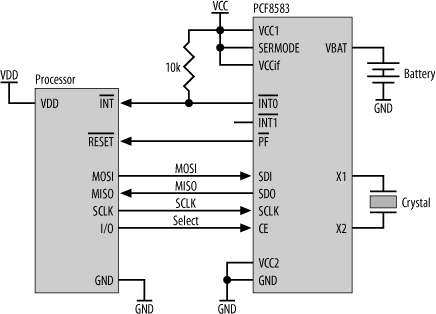
The serial interface of the DS1305 can operate as either a SPI port or a three-wire[*] port. The input SERMODE (SERial MODE) selects which serial mode to use. Connecting SERMODE to the power supply selects SPI operation. Connecting SERMODE to GND selects three-wire operation. (For three-wire operation, SDO and SDI are tied together.) The connection to a microcontroller’s SPI port is straightforward, with MOSI, MISO, SCLK, and a chip select, as we’ve seen previously. There is one important difference, though, for the DS1305. It has an active-high CE (Chip Enable), rather than the more common active-low chip selects of other SPI devices. Therefore, the processor’s I/O line driving CE must be low when the device is not selected and high when the device is selected.
The DS1305 has a special Power Fail (![]() ) output that is asserted low when the primary power source VCC1 falls below the secondary power source (VCC2 or VBAT). This can be used to alert the processor of the power fail (by using it as an interrupt) or to stop the processor (by connecting it to the processor’s
) output that is asserted low when the primary power source VCC1 falls below the secondary power source (VCC2 or VBAT). This can be used to alert the processor of the power fail (by using it as an interrupt) or to stop the processor (by connecting it to the processor’s ![]() ). This is used to prevent a failing processor from corrupting devices as the power dies. If you don’t require a power-fail notification,
). This is used to prevent a failing processor from corrupting devices as the power dies. If you don’t require a power-fail notification, ![]() may be left unconnected.
may be left unconnected.
The input VCCif (VCC for the interface logic) selects the output voltage levels of SDO and ![]() . Since the DS1305 can be used in both 5 V and 3.3 V systems, this input allows the output levels of these pins to be set to the appropriate high voltage. VCCif is just connected to the system’s power supply. Thus, for a 5 V system, VCCif is 5 V, and the outputs of the DS1305 are also 5 V. Similarly, for a 3.3 V system, VCCif is 3.3 V and so are the outputs.
. Since the DS1305 can be used in both 5 V and 3.3 V systems, this input allows the output levels of these pins to be set to the appropriate high voltage. VCCif is just connected to the system’s power supply. Thus, for a 5 V system, VCCif is 5 V, and the outputs of the DS1305 are also 5 V. Similarly, for a 3.3 V system, VCCif is 3.3 V and so are the outputs.
Finally, the DS1305 has two interrupt outputs, ![]() and
and ![]() . These may be used to interrupt the processor when a DS1305 alarm function triggers. As the interrupt outputs are open-drain, they each require a 10k resistor to pull them high when they are inactive. If one or both of the interrupts are not required, just leave them unconnected. Only
. These may be used to interrupt the processor when a DS1305 alarm function triggers. As the interrupt outputs are open-drain, they each require a 10k resistor to pull them high when they are inactive. If one or both of the interrupts are not required, just leave them unconnected. Only ![]() is used in our example, and so
is used in our example, and so ![]() is safely ignored.
is safely ignored.
Finally, the DS1305 has two crystal inputs, X1 and X2. A 32.768 kHz watch crystal is connected across these pins, providing the timing source for the internal clock.
So that is the DS1305, a versatile little chip that can provide timekeeping for your embedded system. It’s easy to use, and the programming information for it is contained in the device’s datasheet.
SPI-Based Digital Potentiometer
Let’s look at another simple SPI example. This time, we will interface a digital potentiometer to a microprocessor. We looked at analog potentiometers in Chapter 4.
Now, a standard pot is manually adjusted. It will either have a knob attached (as in a volume control or brightness adjustment), or it will have a small notch for screwdriver adjustment. Wouldn’t it be great if your microprocessor could adjust the pots in your analog circuits, under software control? That way, your application software could adjust the brightness of the display or change the volume of the sound system. Well, by using a digital potentiometer , you can do just that. Televisions, computer monitors, and stereos with internal embedded controllers use digital pots to adjust settings such as volume. When you hit a volume button on a remote control, the TV or stereo adjusts the settings of digital pots, which are part of the amplifiers driving the speakers.
Figure 7-12 shows an Analog Devices AD5203 digital potentiometer with a SPI interface. This chip has four potentiometers, all of which may be adjusted under software control. Each pot has 64 possible positions, and versions of the chip are available with either 10 kΩ or 100 kΩ impedances. For higher resolution, the pin-compatible AD8403 has a possible 256 settings, also configurable through a SPI interface.
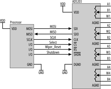
The AD5203 has a Serial Data Input (SDI), which is connected to the processor’s MOSI output. Similarly, the device’s Serial Data Output (SDO) is connected to MISO. The AD5203’s clock input (CLK) is positive-edge triggered midway through each SPI cycle, which means that any processor communicating with it must use high clock polarity and clock phase one on SCLK. The Chip Select (![]() ) of the AD5203 may be driven by a processor digital I/O line. The AD5203 has two other inputs, Shutdown (
) of the AD5203 may be driven by a processor digital I/O line. The AD5203 has two other inputs, Shutdown (![]() ) and Reset (
) and Reset (![]() ).
). ![]() places the device in low-power mode, and
places the device in low-power mode, and ![]() resets the potentiometer wipers to their midpoint. Both of these inputs may also be driven by a processor I/O line, or, if their functionality is not needed, they may be simply tied high using 10 kΩ pull-up resistors.
resets the potentiometer wipers to their midpoint. Both of these inputs may also be driven by a processor I/O line, or, if their functionality is not needed, they may be simply tied high using 10 kΩ pull-up resistors.
The potentiometers within the AD5203 are used as any other pots would be. The A and B terminals connect to either end of the internal resistors, and the position of the wiper (W) is adjusted under software control.
The AD5203 has several ground connections. DGND is the digital ground for the SPI interface and control logic of the chip. The AGNDs are the analog grounds of the internal potentiometers, and they should all be connected to DGND at a single point.
The datasheet for the AD5203 provides the control codes needed to configure the chip, and its use is simple and straightforward.
Adding Nonvolatile Data Memory with SPI
The internal memory of microcontrollers is very small, and their data storage capabilities are severely limited. We’re now going to look at how you can increase the storage capacity of your embedded system by adding an Atmel AT45DB161 2M serial DataFlash using SPI. These chips are commonly used in low-cost digital cameras and answering machines. You could also use this flash chip as a virtual disk drive in your embedded system.
Most other flash chips have a bus interface, but the AT45DB161 has a serial interface, making it well suited for use with small microcontrollers. The AT45DB161 is a 2M chip, but you can get similar chips in capacities ranging from 512K to 32M. They all use the same (or similar) SPI interface, so the same design works for all. (Note, however, that their pinouts and physical packages vary, so one chip will not mount onto a circuit board design for another.)
The chip consists of an array of flash memory, organized as individual pages of 528 bytes each, and two RAM buffers, also 528 bytes each (Figure 7-13). To write data into the main flash array, the processor must first write data into one of the buffers and then issue a command to write that buffer into the array. A processor can read the contents of either of the buffers, transfer a flash page to the buffers, or read from the flash array directly. The operation of the buffers is independent, and one buffer may be accessed by the processor (via SPI) while the contents of the other buffer are being written into the flash array.
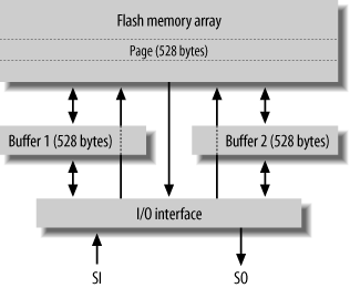
The flash supports numerous commands for writing to and reading from the buffers, writing the buffers to the main array, and transferring an array page back to a buffer. The Atmel datasheet has full details of the software protocols and command set.
There are a few things to note about the internal architecture and the flash array. The first is that one 528-byte page of the flash array is not contiguous with the next. In other words, if you are using a pointer in your software to track the current location in the memory, you can’t just increment it from the end of one page and expect it to be pointing to the next. Every 528 bytes (and it’s a strange number), you have to leap forward to the next page. Think of it as pages of 528 bytes with big gaps in between.
The second catch with this memory is that it has a lifetime of only 1,000 write cycles per page. Most flash technologies (and there are several different types) support 100,000 write cycles or better, and you can normally exceed this limit and the device will keep working reliably for you. This isn’t the case with the AT45DB161. Once the 1,000-write limit is exceeded, memory locations will start failing on you. The chip will read existing data back correctly, but new pages will not write successfully. Depending on the application, this limit may not be a problem. I’ve used this particular chip in my design for long-duration data loggers. These machines are deployed for yearlong deployments, collecting (and compressing) data and storing it away in the flash chip. The logger gradually builds a page image in one of the buffers before storing it to the array in a single write. Since during a deployment, a page will be written only once (and then the logger will move on to the next page), the 1,000-write limitation isn’t a problem. It would take 1,000 deployments before the chip would fail. However, if you’re using the chip for variable storage and are modifying the flash pages on a byte-by-byte basis, you’re in trouble. Individually changing 528 bytes within a page counts as 528 writes. So do that twice to a page, and suddenly you’re over the limit. Therefore, this flash is well suited to some applications and not others.
The basic design for using an AT45DB161 is shown in Figure 7-14.
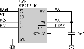
On the left of the chip are the SPI interface connections, MOSI, MISO, SCK, and a chip select (FLASH). The chip will support SPI transfers at up to 20 MHz, so the SPI interface can be run very fast indeed. On the right of the chip is the power supply, VDD, which is decoupled to ground using a 100 nF capacitor. The AT45DB161 requires a power supply in the range 2.5 V to 3.6 V. However, its logic inputs are 5 V tolerant, meaning this chip can be used in systems with mixed power supplies. In other words, while this chip requires a 3 V power supply, it can be directly interfaced to a processor with a 5 V supply (and 5 V logic levels). The AT45DB161 has a write-protect pin (![]() ), which, when driven low, prevents the contents of the flash from being modified. If you don’t require write protection, simply tie this input high, as shown in the schematic. The flash also has a
), which, when driven low, prevents the contents of the flash from being modified. If you don’t require write protection, simply tie this input high, as shown in the schematic. The flash also has a ![]() input so that the chip can be manually reset under software control. The flash incorporates an inbuilt power-on reset that will put the device into a known state, and therefore a “manual” reset at power up should be unnecessary. However, I’ve found that the internal power-on reset generator is somewhat finicky and doesn’t always kick in as it should. Under such circumstances, the flash fails to enter a known state and is unusable in the system. Therefore, I have found it good practice to give the processor control of the flash’s reset. As part of the processor’s initialization routines executed in its reset firmware, I get the processor to reset the flash, nudging it into reality. It’s a simple thing, but it makes all the difference for a reliable system. Pin 1 is a status output (RDY/
input so that the chip can be manually reset under software control. The flash incorporates an inbuilt power-on reset that will put the device into a known state, and therefore a “manual” reset at power up should be unnecessary. However, I’ve found that the internal power-on reset generator is somewhat finicky and doesn’t always kick in as it should. Under such circumstances, the flash fails to enter a known state and is unusable in the system. Therefore, I have found it good practice to give the processor control of the flash’s reset. As part of the processor’s initialization routines executed in its reset firmware, I get the processor to reset the flash, nudging it into reality. It’s a simple thing, but it makes all the difference for a reliable system. Pin 1 is a status output (RDY/
![]() ) indicating whether the device is ready or if it is still completing an internal operation.
) indicating whether the device is ready or if it is still completing an internal operation.
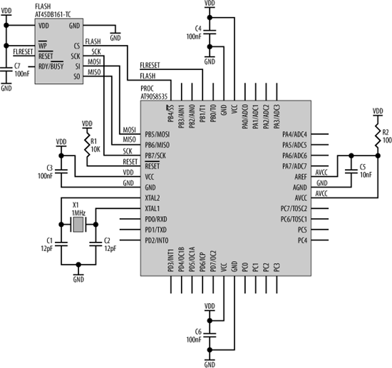
The connections for interfacing this memory chip to an Atmel 90S4434 AVR processor are shown in Figure 7-15. The AVR portion of the schematic is no different from the examples we have seen previously. That’s the nice thing about simple interfaces such as SPI. They form little subsystem modules that “bolt together” like building blocks. Start with the basic core design and just add peripherals as you need them. The schematic also shows decoupling capacitors for the power supplies, the crystal oscillator for the processor, and a pull-up resistor for ![]() . Pin 41 (PB1) is used as a “manual” (processor-controlled) reset input to the flash.
. Pin 41 (PB1) is used as a “manual” (processor-controlled) reset input to the flash.
Adding a Parameter Memory Using SPI
We saw in the previous section how to add a large-capacity serial flash for data storage. It is often useful to use nonvolatile memory to hold system parameters, a way of preserving important variables during periods of no power. But the AT45DB161 DataFlash is just not the device for that task. It is better suited to data recording, and its large capacity is overkill for parameter storage. So, now we’re going to look at how you can use SPI to add a small parameter memory (in the form on an EEPROM) to your embedded system. The EEPROM I’ve chosen is the Atmel AT25640. This device will hold data for at least 100 years without power, and will endure more than one million write cycles (significantly more than an AT45DB161!). As such, your software can happily alter parameter variables without fear of limiting the lifespan of the chip. The AT25640 has only 8K of memory, which might not sound like much. But don’t forget, that’s 8192 char variables, which is more than enough storage space for most parameters. If 8K is too much, there are also versions of the chip with 1K (AT25080), 2K (AT25160), and 4K (AT25320) bytes of memory.
The architecture and use of the AT25640 is much simpler than that of the AT45DB161. Full details of the required software protocol are in the Atmel datasheet for this chip.
The schematic for an AT25640 circuit is shown in Figure 7-16.
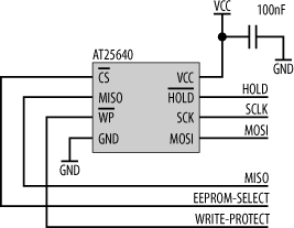
The interface is standard SPI, and the chip also has a write-protect input and a hold input. Asserting HOLD allows the processor to temporarily stall a serial transfer (while it performs other tasks) without terminating the access to the AT25640. And as you might expect, write-protect, when asserted, turns the chip into a read-only device. These control inputs may be driven by programmable I/O lines of the processor. The only other requirement is power (which is decoupled to ground using a 100 nF capacitor) and ground. The chip is available in two types. One will operate from a supply voltage of between 2.7 V and 5.5 V, while the other needs a supply voltage of between 1.8 V and 3.6 V.
[*] Developed by National Semiconductor, three-wire, also known as MicroWire, is very similar to SPI and is found is some microcontrollers and DSP processors. Unlike SPI, which has separate data lines for reading and writing, three-wire uses a common bidirectional data line.