
Power electronic circuits for magnetic bearings
In magnetic suspension controllers, current or voltage commands are generated via the sensing of the displacement of a suspended object. Power electronic circuits apply voltage to the winding terminals to produce current in the windings. The rate of change of current should be fast enough to follow the current command. However, the amplitude and frequency ranges are limited by the voltage and current ratings of the power electronic circuits and the bearing winding inductances. If the current response is not fast enough, then the feedback loop becomes unstable, which results in shaft touch-down.
In this chapter, the structures and principles of power electronic circuits are explained (focusing on switched-mode amplifiers) and the principles of pulse width modulation (PWM) are introduced. For a PWM scheme, the linear and nonlinear current regulations are shown. The limitation of amplitude and frequency range of current supply is derived, with a brief introduction of IGBT and MOSFET power devices as well as gate drive circuits.
5.1 Structure and principles of power electronic circuits
Table 5.1 shows typical voltage and current regulators for magnetic bearings. Linear analogue amplifiers have push–pull transistors at the output stage, as shown in Figure 5.1(a). This circuit is often used in audio amplifiers. Basically, push–pull circuits amplify the current capability. In addition to the current capability enhancement, a high-gain linear amplifier can be integrated, such as a power operational amplifier. Voltage or current followers can be constructed with external resistor circuits. The linear amplifiers have the advantage of precise current and voltage regulation as well as low noise and they have a current rating of less than 10 A. Operation at the rated current is available only with effective cooling. Cooling of the output stage transistors is done with large heat sinks. Therefore the amplifier dimensions are large, resulting in high cost. The efficiency is low because of high losses in the push–pull transistors.
Table 5.1
Voltage and current regulation
| Advantage | Disadvantage | |
| Linear analogue amplifier | Precise regulation | High cost |
| Low noise | Low efficiency | |
| Large dimension | ||
| Switched-mode PWM amplifier | High efficiency | Noise generation |
| Compact Low cost | ||
| Hybrid amplifier | Precise regulation Better efficiency | Difficult to set operating point |
| Better efficiency |
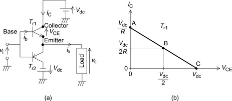
Figure 5.1 Push–pull transistors and operating points: (a) push–pull transistors; (b) operating points
Switched-mode amplifiers enhance efficiency. Since the losses in the power devices are reduced the heat sinks are much smaller and, as a result, switched-mode amplifiers are compact in dimension so that the cost is low. Switched-mode operation of power devices is widely used in industry, e.g., for general-purpose inverters in ac drives and computer power supplies. Domestic appliances, most air conditioners, high specification refrigerators and washing machines use switched-mode power inverters to improve efficiency. Hence switched-mode amplifiers are dominant in magnetic bearing drivers.
Hybrid amplifiers take advantage of linear and switched-mode amplifiers. At low current the push–pull transistors operate as a linear amplifier but at high current they operate in switched mode. To take advantage of a hybrid amplifier, it is quite important to modify the winding structure in magnetic bearings.
5.1.1 Linear transistor amplifiers
Figure 5.1(a) shows the circuit configuration of the push–pull amplifier. Positive and negative dc voltages are supplied. The output voltage νo follows the input voltage νi, and if νi is sinusoidal then νo is also sinusoidal with the same amplitude. The current drive capability is increased by the collector current gain hFE, which is normally in the range of 20–100, e.g., a base current ib of 0.1 A is required for an output current io of 5 A if hFE = 50.
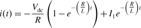
Figure 5.1(b) shows the possible operating points of Tr1 on the voltage and current plane. The possible operating points are on the line ABC. At point A, Tr1 is on so that the collector–emitter voltage VCE is almost zero with the maximum collector current IC, i.e., Vdc/R, where R is a load resistance. The device power consumption is almost zero. The operating point moves along the load line as VCE is increased. At point B, IC and VCE are half of the maximum current and voltage so that the output voltage νo = Vdc/2. The power consumption of Tr1 is a product of VCE and IC so that Tr1 = V2dc/4R. The operating point travels towards point C if νo further decreases. At point C, νo is minimum, and io is zero, i.e., Tr1 is off. The power consumption in Tr1 is zero. One can draw a similar load line with negative voltage for the transistor Tr2.
In linear amplifiers, the operating points travel along the load line and considerable power is consumed by the transistors because they are neither fully on nor fully off. Only at operating points A and C the power consumption is zero. The principle of switched-mode amplifiers is that the operating points are always set to A or C to minimize losses. Therefore the output voltage is not continuous but has two discrete values, i.e., +Vdc or −Vdc. The required voltage value is somewhere between +Vdc and −Vdc so that the time lengths of operating points (i.e., the “on” and “off” times) are adjusted so that the average voltage corresponds to the reference voltage. The details are explained in the section “PWM Operation”.
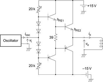
Figure 5.2 shows the circuit configuration of a linear amplifier with two stages. An oscillator is connected to the push–pull amplifier to drive the transistors and apply a voltage to the winding terminals. The oscillator can be replaced with operational amplifiers or D/A converters. It may be thought that an oscillator may be connected directly to the winding terminals to apply the voltage; however, voltage reduction occurs because of the output impedance. This is explained below.
General-purpose oscillators, D/A converters and operational amplifiers usually have an output impedance of several hundred ohms with an output voltage range of −12V to +12V. Let us consider a sinusoidal waveform. If the output terminals of the oscillator are opened then a sinusoidal waveform, having amplitude of 12V, can be obtained. However, if an electrical circuit with low input impedance is connected to the oscillator terminals, the output voltage amplitude is decreased. The oscillator output voltage νi is written as
where νosc is the open-circuited voltage amplitude, Zo is the output impedance of the oscillator and Zi is the input impedance of an electrical circuit connected to the oscillator output. For example, the amplitude is reduced to 6V if the input impedance is the same as the output impedance of the oscillator. Hence if the winding has an impedance of only a few ohms then the output voltage amplitude is reduced significantly. Therefore the reduction of output impedance is important. In most cases, the input impedance of the connected circuit is designed to be high enough to make the output impedance negligible so that νi is almost equal to νosc.
The two-stage amplifier circuit reduces the output impedance. In one transistor, the collector current is amplified by hFE times the base current. Therefore the required input current iosc is written as
where hFE1 and hFE2 are the current gains in transistors 1 and 2. For example, if io = 1A, hFE1 = 100 and hFE2 = 60 then iosc = 1.6 mA. Hence the input impedance of the 2-stage amplifier is 12 V/1.6mA = 7.5 kΩ, which is sufficiently high compared with the output impedance of the oscillator.
The adjustable 20 kΩ resistors set the bias dc current for less waveform distortion and the series diodes compensate the voltage drop between base and emitter terminals. The first stage transistors are low current types; however, the second stage transistors have a high enough current rating for the load current. For example, a maximum current rating of 5 A is usually required for a 1 A load current and heat sinks are required for the second stage transistors.
5.1.2 Linear operational amplifiers
Transistor amplifiers with push–pull circuits can be integrated into one package with the differential amplifiers. These semiconductor devices are sold in the market as power operational amplifiers. General-purpose operational amplifiers can drive output currents between 10 and 30 mA. However, the rated current for a power operational amplifier is usually between 1 and 10 A. Normally an effective cooling method is required to operate at the rated current. In most cases, de-rating is necessary to match the heat sinks and airflow.
A voltage follower circuit is easily fabricated from a power operational amplifier. The negative input is connected to the output and the positive input is connected to the input voltage νi. The output voltage νo follows the input voltage νi. However, the voltage gain is unity and current drive capability is increased.
Figure 5.3 shows a linear current driver using a power operational amplifier. The output current io is following the input voltage νi. If the gain is set to unity then 1 A of current is provided at an input voltage of 1V. The resistance R6 has a low value to avoid losses because the main current flows through it. The other resistances R1, R2, R3 and R5 have values in the range of several kΩ. The relationship between the input voltage and output current is written as
In the case of resistance values given in the figure, the current gain is unity. In designing the current driver, the value of R6 should be determined by considering the load resistance, supply voltage, heat generation in power operational amplifier and R6. It should be noted that the resistors should have low temperature drift and wide frequency range. Noise and high frequency oscillation should be avoided with practical wiring and smoothing capacitors.
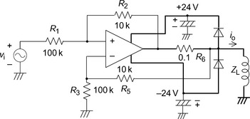
The diodes provide a regenerative current path for the inductive load. The output voltage is limited to the power supply voltages. Chemical capacitors are necessary in parallel with the power supply to maintain the power supply voltage in case of sudden increase of output current. In addition to the chemical capacitors, ceramic capacitors with a high frequency range are also necessary, as with most electrical circuits.
Figure 5.4(a) shows an output stage of a transistor circuit with a load resistance of 10Ω and supply voltage of ±100 V.
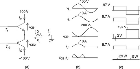
Figure 5.4 Linear and switched-mode operations: (a) output stage; (b) linear operation; (c) switched-mode operation
1. Suppose that the output voltage is sinusoidal with maximum amplitude. Draw the waveforms for the load voltage νL and current iL, as well as voltage νCE1 and current iC1. Also draw the instantaneous power consumption in Tr1. Derive average power consumption of Tr1.
2. Suppose that the transistors are operating in switched mode, and the output voltage has a square waveform. Draw the waveforms and derive the average power consumption of Tr1 assuming that the voltage drop for the on state of the transistors is 3 V.
3. Efficiency is defined as the ratio of load power consumption to the power provided by the DC source power. Derive the efficiency for the cases of linear and switched-mode operations.
4. How much power is consumed in linear operation compared to switched-mode operation?
Figure 5.4(b) shows the waveforms for linear operation. The load voltage and current are sinusoidal and Tr1 supplies current in the positive half period. The transistor voltage νCE1 is given as
Instantaneous power consumption is the product of νCE1 and ic1, i.e.,
as shown in the figure. Therefore average power consumption is
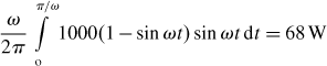
In switched-mode operation, the waveforms are shown in Figure 5.4(c). A transistor on-state voltage drop of 3 V is assumed. Therefore the output voltage amplitude is +97 V or −97 V and the peak value of the load current is +9.7 A or −9.7 A. The power consumption in Tr1 over a half cycle is the product of 3 V and 9.7 A, i.e., 29 W. Hence the average power consumption is 15W.
In linear operation, the load power consumption is ![]() . The supplied power from the power source is the sum of load power and transistor power losses = 500 + 68 + 68 = 636 W, giving an efficiency of 500/636 = 78.6%.
. The supplied power from the power source is the sum of load power and transistor power losses = 500 + 68 + 68 = 636 W, giving an efficiency of 500/636 = 78.6%.
In switched-mode operation, the load power consumption is 97 × 9.7 = 941 W. The supplied power is a sum of load power and transistor loss = 941 + 15 + 15 = 971 W, giving an efficiency of 941/971 = 97%.
The power consumption ratio is 68/15 = 4.5. Note that switched-mode operation results in significantly less power consumption in the semiconductor devices. Small heat sinks with less airflow are therefore required so that small and lightweight voltage and current drivers can be used. It should be noticed that if the voltage is increased, but the current is decreased to maintain the same power, then the efficiency is higher. Increasing the number of coil turns by using thinner wires will increase the coil impedance allowing for high voltage operation. Also, if the voltage drop during the on state is decreased, more efficient drivers are obtained. Recent power device developments have led to the voltage drop during the on-state in IGBTs to decrease down to about 1.6 V. MOSFETs provide low device losses with low on-state resistance in low voltage circuits. For further power consumption calculations, switching losses should be included with the on-state power consumption.
5.1.3 Switched-mode amplifiers
In this section, three types of switched-mode amplifiers are introduced. The first is a single-phase H-bridge inverter; the second is a simplified single-phase inverter for unidirectional current. This inverter is widely used in magnetic bearings. The third is a chopper circuit for low voltage and current drivers.
Figure 5.5 shows the two main circuits that are used in a single-phase inverter. In Figure 5.5(a), four power-switching devices (e.g., IGBTs) are connected in an H-bridge configuration. The power-switching devices can be other self-turn-off devices such as MOSFETs, transistors, SITs, and so on. These power-switching devices are encapsulated with an anti-parallel diode. The magnetic bearing winding is represented by an inductor and the terminal voltage and current are νL and iL, respectively. The circuit operation has several modes depending on the current direction and on–off states of the switching devices.
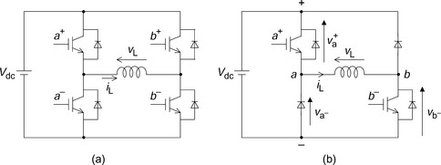
Figure 5.5 Single-phase inverters: (a) single-phase inverter; (b) single-phase inverter with unidirectional current
Figure 5.6 shows the operation modes. In modes 1 and 2, the gate voltage is applied to IGBT a+ and b−. If the winding current is positive then the current flows from positive dc terminal, through IGBT a+, the winding and the IGBT b− and returns to the negative dc terminal as shown in mode 1. If the winding current is negative, current does not go through IGBTs a+ and b−; instead, the current goes through the anti-parallel diodes of a+ and b− so that the stored magnetic energy in the winding flows back into the dc power source. In modes 1 and 2, positive voltage is applied to the winding terminals and the current path is automatically changed depending on the winding current direction.
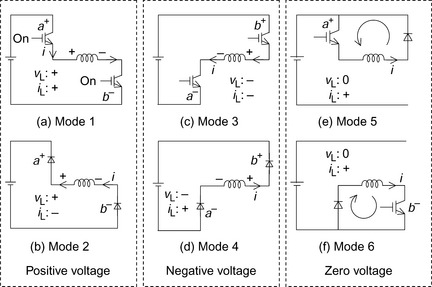
In modes 3 and 4, negative voltage is applied to the winding terminals. The gate voltages are applied to IGBTs a− and b+. Depending on the current direction of the winding, the current path is as in mode 3 or 4.
One may notice that the single-phase inverter is designed to provide positive and negative voltage as well as bidirectional current flow. In magnetic bearing controls that utilize bias current, only unidirectional current is required. Suppose only positive current is required, then modes 2 and 3 are not necessary. Hence the single-phase inverter can be simplified as shown in Figure 5.5(b).
Diodes can replace IGBTs a− and b+. This simplification reduces the cost, so this circuit is widely used in magnetic bearings. For one radial magnetic bearing with two-axis active positioning, four electromagnets are constructed, hence four inverters with eight wirings are required and, in total, eight switching devices are necessary (down from 16 when using full H-bridge inverters). This circuit configuration is also used widely in switched reluctance motor drives. However, these power modules are not widely available on the market in 3-phase inverter form.
Figure 5.6(e,f) shows additional modes, i.e., the zero-voltage modes. In these modes the winding terminal voltage is almost zero. They are useful for reducing the switching frequency. In mode 5, gate voltage is applied to only the a+ switching device. The winding current circulates through the diode and a+ device providing a short-circuit path. In mode 6, switching device b− is on, providing a short-circuit path with another diode. In the zero-voltage modes, the winding current is almost constant. These modes of operation are often described as freewheeling.
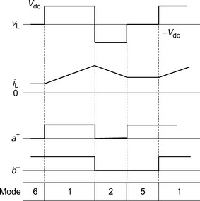
Figure 5.7 shows an operating sequence, including the zero-voltage mode. In mode 1, gate voltages a+ and b− are high so that the IGBTs are on. The load current iL increases as positive voltage is applied. In mode 2, the diodes are on so that the winding current decreases due to negative voltage being applied. In mode 5, the current value is kept constant and zero voltage is applied to the terminals.
5.1.4 Low cost chopper circuit
In some applications, cost reduction is more important than efficiency and performance of the power electronic circuits. This is especially true in small voltage and current applications where the minimum number of switching power devices should be used for cost reduction. A drop in efficiency is allowed because the voltage and current are not high. In these applications, a chopper circuit (which is basically a dc-to-dc converter) with variable voltage is employed.
Figure 5.8 shows the main circuit of a chopper circuit. Only one switching power device is required for one winding. There are two operating modes. In mode 1, the switching device is turned on and positive voltage is applied to the winding. In mode 2, the switching device is turned off, and a zero voltage loop occurs through the diode and winding (freewheeling again).
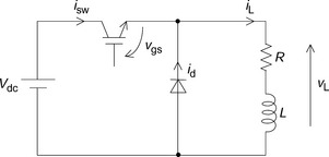
Figure 5.9 shows the operating sequence for the chopper circuit. In mode 1, the winding voltage νL is positive and the current iL increases. The on-state voltage νgs of the switching device is high and the winding current isw is flowing through the switching device. In mode 2, the current iL is almost constant since the winding is short-circuited.
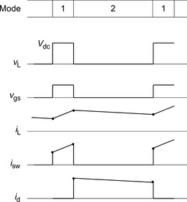
The main problem associated with the chopper circuit is easily understood from the waveforms. A fast increase in winding current is possible in mode 1; however, during mode 2 (zero voltage) the current decay is quite slow. The current decay leads to energy dissipation via winding loss and diode voltage drop. Unsymmetrical current response characteristics result in a nonlinear transfer function of the current regulator. The nonlinearity may cause a stability problem with the negative feedback loops in a magnetic suspension system. To enhance the current response, one solution is to connect a resistor in series with the winding. In zero voltage mode, the current decreases as a function of exp(−Rt/L), where R is the sum of a winding resistance and a connected resistor. Therefore an increase in R results in a fast current decay. Moreover, the rate of change of current increase is reduced because of the voltage drop at the resistor terminals. Therefore an external resistor compensates for the unsymmetrical current response to some extent. The disadvantage is the additional power consumption in the resistor.
The other way to enhance the response of current decay is to connect the external resistor in series with the freewheeling diode. The loss in the resistor is decreased because resistor current is only present during the zero-voltage mode.
With considerable trade-off in the design a low cost power electronic circuit is possible for low voltage and current applications.
5.2 PWM operation
In this section, the operation of a single-phase inverter with unidirectional current is analysed and discussed. First, the principles of PWM are explained. Then an analysis of voltage and current is carried out and the derived voltage and current relationships are applied to a magnetic bearing example. A calculation method for the winding resistance is shown in order to obtain the time constant. The example is also analysed by computer simulation for better understanding.
5.2.1 Principles
Figure 5.10 shows the principles of PWM operation in a single-phase inverter with unidirectional current. The triangular waveform νc has a frequency of fc and the maximum and minimum values are +1 and −1, respectively. The voltage command is ν* and a comparator provides a digital signal νcom from the comparison of νc and ν* as shown in the figure. Using the comparator output signal the switching devices are operated. If νcom is high then the switching devices are turned on so that the dc bus voltage Vdc is applied to the winding. On the other hand, − Vdc is applied when νcom is low.
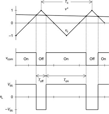
Let us define the carrier period and the on and off periods as Tc, Ton and Toff respectively. Therefore the average output voltage in winding terminals is
where
In addition, the relationship between the voltage command and the on-to-period ratio (the duty cycle) is written as
Substituting these equations into (5.4) yields
This equation indicates that the voltage across the winding terminals is proportional to the voltage command. The winding voltage can be controlled by the voltage command when the dc bus voltage Vdc is kept constant. The voltage can be both positive and negative. Note that a dead time, which is normally required in a typical inverter, is not needed. Therefore better linearity is obtained.
5.2.2 Analysis of RL circuit
A magnetic bearing winding can be represented by a series R-L circuit. When the dc voltage Vdc is applied as a step function, the voltage and current equations can be obtained using the Laplace transform:
where I0 is the initial current. Solving the equation for I(s) and transforming into the time domain provides the current:
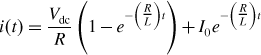
The first term gives the current component due to the applied voltage. The second term is obtained from the initial current.
For the negative voltage period, substituting −Vdc into the above equation gives
where I1 is the initial current of the negative voltage period.
For the radial magnetic bearing shown in Figure 2.14 derive and calculate the following:
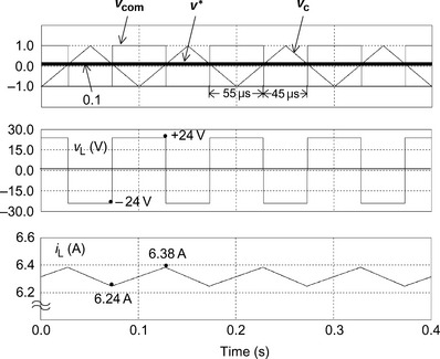
3. Suppose that the PWM carrier frequency is 10 kHz with Ton = 55 μs and Vdc = 24 V. Find the current values at the switching points in the period. Also find the average current value.
4. Draw the waveforms for the triangular carrier signal, voltage command, comparator output, terminal voltage and winding current by a digital simulation.
1. The conductor cross-sectional area S is given as a product of the wire cross-sectional area and the number of parallel strands, i.e., Nst = 2, so that
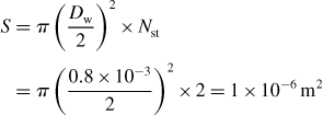
where Dw is the diameter of a wire.
Let us assume that the length of the straight coil part is the sum of the iron core stack length l and an additional length lad of 4.5 mm at the both ends. The coil end is assumed to be a semicircle of diameter Dend. The wire length is the sum of the straight and circular lengths. The straight length Lst is
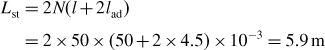
Figure 5.11 shows an enlarged figure of iron core cross section. The conductors fill the shaded area in the stator slots. To simplify the calculation, let us assume that the coil-end diameter Dend is equal to the arc between the slot coil centres so that
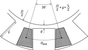
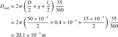
Therefore the wire length of the circular part of the coil is
Hence the total length of wire in a phase coil is
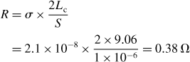
Two coils wound around neighbouring magnetic poles are connected in series so that the total wire length is 2Lc. The resistivity of copper σ is 2.1 × 10⁻⁸ Ωm at a temperature of 75 °C. Therefore the resistance is
2. The time constant is given as a ratio of inductance and resistance
3. From (5.9), the current I1 can be obtained after 55 μs of positive voltage application using
And also the current value at the end of the negative voltage mode, from (5.10), is
Substituting I1 given in (5.18) into (5.19) and solving for I0 gives
Substituting I0 into (5.18) yields
Hence the current values at the switching instances are derived. The instantaneous current values can be obtained from (5.9) and (5.10) by substituting I0 and I1.
The average current value can be derived from the integration of the instantaneous current waveforms; however, there is a simple way to obtain the average current from the average voltage. The average voltage is calculated from (5.4) so that
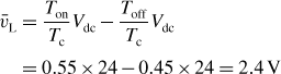
The average current is obtained by dividing the average voltage by the resistance
4. The top graph of Figure 5.12 shows the waveforms for carrier signal νc, voltage command ν* and comparator output νcom. In the middle graph the winding terminal voltage νL characteristic is illustrated while the bottom graph shows the winding current waveform. The power electronic simulation is carried out using the PSIM program, which is a fast, efficient and cost-competitive digital simulation program for modelling power electronic circuits, including switches and controllers.
5.3 Current feedback
In the previous chapter, inverter and chopper operations were introduced and discussed. The single-phase inverter with unidirectional current direction is often used in magnetic bearing applications so this chapter focuses on the operation of this inverter configuration.
A high frequency response is required in a magnetic bearing system. Therefore current feedback is necessary for fast response. Moreover the current feedback compensates for the problems associated with the following characteristics:
1. A transfer delay of 1/(R + sL) is caused by the winding resistance and inductance.
2. The switching speed of the power devices used in inverters is limited. This switching delay causes a nonlinear transfer function between the voltage command and output voltage of the inverter.
3. The output voltage of the inverter drifts if the dc supply voltage varies.
4. The voltage drop across a switching device when turned on is not zero. The on-state voltage drop results in a nonlinearity in the voltage transfer function.
5. A temperature drift of winding resistance causes a time variant system.
In order to suppress the influence of these problems, current feedback is usually employed. The current feedback strategies are as follows:
1. A linear current controller.
2. A nonlinear current controller such as a hysteresis function or a delta modulation controller, etc.
In this section, the characteristics of a linear current controller are discussed first, followed by a description of a nonlinear controller.
5.3.1 Linear current controller
Figure 5.13 shows a block diagram of a linear current controller system. The current iL is detected then compared with the current command i*L. The current error ie is amplified by a controller block Gc and, from the current controller, a voltage command ν* is generated. A limiter block keeps the voltage command within the PWM triangular carrier waveforms. In the Ginv block, the on-and-off logic for the main power devices is determined and the voltage is applied to the winding. The winding transfer function is simply represented by 1/(R + sL) and the current iL is the output. The transfer function of this feedback loop is then

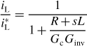
This equation indicates that the transfer function is close to unity if GcGinv is high. However, a gain limitation exists because of the limited switching frequency.
Let us look at the current regulating characteristics from computer simulation. In the simulation, the main circuit current is detected and a high-cut filter provides current feedback signal, which is compared with the current command. A proportional and integral (PI) controller, having proportional gain KPI and integrator time constant TPI, amplifies the current error so that the output is limited to between −1 and 1. This is the amplitude of a PWM triangular waveform. The limiter output, i.e., feedback voltage ν*, is compared with a PWM carrier triangular waveform at 10 kHz. The comparator output logic is fed to the main power-switching devices.
Figure 5.14(a–g) shows the current waveforms. The waveforms are plotted from 0.5 ms in order to see the steady-state conditions. To observe the transient response, the current command is decreased and increased at 1 and 2 ms, respectively. In this simulation the zero-voltage loop is not used. The waveforms show the current command and winding current. The current waveform includes a triangular component, which is often called the current ripple. In Figure 5.14(a), the current command has a step function change from 4 to 3.9 A at 1 ms. With the effect of feedback, the current follows the command after a 0.5 ms transient period. A similarly good response is also seen after the step at 2 ms. Hence it is found that the current response is good with a small step change of the current command.
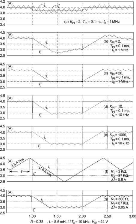
Figure 5.14(b–g) shows the current response when the current command has a large step change. The current command is decreased from 4 to A at 1 ms, then increased back to 4A at 2 ms. Just after the step command, the feedback voltage is saturated so that the winding terminal voltage is fixed to the minimum value for a period. The current has a ramp function decrease. In Figure 5.14(b) it can be seen that it takes about 0.4 ms to follow the current command. The current slew rate is determined by the applied voltage and also the winding inductance. To enhance the current slew rate, an increase in inverter dc voltage is necessary. In addition, after reaching the current command at a time of 1.3 ms, the current then overshoots the target command. To improve the current response the gain of the proportional controller should be increased.
Figure 5.14(c) shows the waveforms with KPI = 20, which is 10 times that of the original controller. It is seen that the current response is much faster in the time range of 1.4–1.7 ms compared with the previous figure. However, voltage command ν* includes high frequency oscillation. This oscillation causes abnormal switching which increases the switching frequency so that it may cause excessive heat generation in power devices. The high frequency oscillation should be removed with a high-cut filter.
Figure 5.14(d) shows the effect of the high-cut filter with a cut-off frequency of fh = 10 kHz. The voltage command ν* does not include a high frequency component; however, a 10 kHz sinusoidal ripple is added. The current response is now excellent, at around 1.4–1.7 ms in this simulation.
In Figure 5.14(e) the proportional gain is increased significantly. Now there is no abnormal switching of the triangular function and the current response is excellent. The feedback voltage is mostly saturated. Even though the current follows to the command in a time range of 1.5–2 ms, the feedback voltage is saturated. This operation is very close to the nonlinear current control method.
In this section, the linear current feedback method was introduced. The current response is good for large step response with an increased proportional gain and a high-cut filter. If the proportional gain is significantly increased then the operation is close to the nonlinear feedback method.
5.3.2 Non-linear current controller
Figure 5.15(a–c) shows the principles of a hysteresis current controller. In Figure 5.15(a), the detected current iL is compared with the current command i*L so that the error ie is obtained. From the current error, a hysteresis block generates an on-off command for the main power-switching devices.
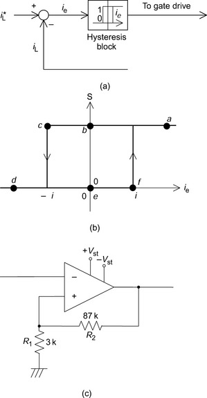
Figure 5.15 Hysteresis current regulator: (a) hysteresis current controller; (b) hysteresis function; (c) hysteresis comparator with operational amplifier
Figure 5.15(b) shows the function of a hysteresis current controller. The horizontal axis is the current error as an analogue function. The vertical axis is the output digital signal, which takes a value of 0 or 1. Let us define the digital signal as S. This is 1 if ie > Δi and 0 if ie < − Δi. If the absolute value of ie is less than Δi then S is left unchanged from the previous value.
Suppose that ie is at the operating point a. If ie is decreased gradually, the operating point travels from a to b and then to c. If ie is decreased further then S becomes 0. Next, let us suppose that the operating point is at d. If ie is increased, the operating point travels from d to e and then to f. If ie is increased further, then S becomes 1.
Figure 5.16 shows the waveforms of a hysteresis current controller. The upper figure shows the current command i*L as a solid curve while i*L + Δi and i*L − Δi are dotted curves. The middle and the lower graphs show the current error ie and on-off logic S. Suppose that the original operating point is a; as the current value is less than i*L − Δi, S is 1. If a positive voltage is applied to the main circuit then current increases rapidly and the operating point moves from a to b and then to c. At the operating point c, S becomes 0. Since there is a delay in the power devices, a negative voltage is applied to the winding terminals at d so that the current decreases when moving between points e, f and a.
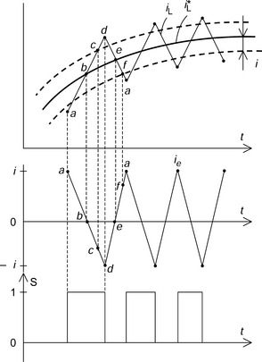
Note that the current waveform is composed of straight lines connecting at the switching points (i.e., a linear approximation of the circuit). The change of current can be written as
where Vdc is the peak value of applied voltage, L is the winding inductance and t is time. This equation is valid only when the switching frequency is high with respect to the time constant of the RL circuit.
A hysteresis current controller is regulating an RL series circuit current with hysteresis widths of 0.5 or 0.05 A, and a current command of 4 A at t = 0. The current command is decreased to 3A at 1 ms then increased to 4 A at 2 ms. Sketch the current waveform. The dc voltage of the inverter is 24V and load inductance is 8.6 mH. Also derive the switching frequency in steady state. Construct a hysteresis function using an operational amplifier and resistors. Construct the digital simulation blocks and show the current waveforms.
From (5.25), the rate of change of current is given as Vdc/L = 2.8 A/ms. Figure 5.14(f) shows the current waveform for the case of Δi = 0.5 A. Although it is not drawn, the current is zero at t = 0. A line is drawn having that slew rate. The line has an intersection with i*L + Δi, at which point the current rate is changed to −2.8 A/ms. The second line has an intersection with i*L − Δi at t = 0.6 ms as shown. Then the current is increased up to 4.5 A at t = 0.9 ms where it is switched again and decreases down to 2.5 A at t = 1.7 ms. During this period the current command has a step-function change.
In the figure, ΔT is defined as a term of half cycle. Substituting iL = 2Δi and t = ΔT into (5.25) then
One cycle termination Ts is 2ΔT and the switching frequency fs is an inverse function of Ts so that Substituting values, fs = 1.4 kHz.
Figure 5.15(c) shows a hysteresis comparator circuit formed from an operational amplifier and resistors. The resistors R1 and R2 determine the hysteresis width. Let us suppose that a saturation voltage of the operational amplifier output is Vst. Hence the hysteresis voltage Δν is
Suppose that the current detection gain is Kig so that the current function is converted into a voltage function using ν = Kig iL. Therefore the hysteresis current width is obtained from
Substituting Kig = 1, R1 = 3kΩ, R2 = 87 kΩ, Vst = 15V then Δi is 0.5A.
Figure 5.14(g) shows the current response with R1 = 300Ω. The current hysteresis is 0.05 A. Hence we get a fast response and small error.
5.4 Current driver operating area
In the previous section, current control strategies were investigated in order to improve the system response. However, it was shown that the slew rate of the current was limited by the dc supply voltage of the inverter. This fact indicates that the operating frequency range of a current driver is limited. At a low frequency the output current is limited by the rated value, which is determined by power devices and dc power source. At high frequency the maximum output voltage limits the current response. If a current, with frequency ω and amplitude Ip, is required then the inverter should have an output voltage of ωLIp, where L is the inductance of a winding. Since the inverter output voltage is limited, the possible current amplitude decreases and is inversely proportional to ω.
In a magnetic bearing system, the current driver operating area should be wide enough for the requirement. If the current command, generated by the radial positioning loop, is outside the operating area then the current driver is saturated and the negative feedback is opened, producing unstable radial positioning. This is because the magnetic suspension system is inherently unstable; so it is quite important to check the operating area of a current driver well in advance.
5.4.1 Operating area
Figure 5.17(a) shows the definition of the operating area of a current driver. The horizontal axis has a logarithmic frequency scale. The vertical axis is the current amplitude and also has a logarithmic scale. At low frequency the operating area is limited by the current rating. However, the voltage limitation line, which has an incline of −20 dB/dec, provides the high frequency current limit. Hence the operating area is the shaded area.
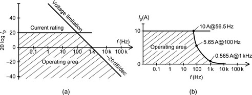
Figure 5.17 Current drive operating area: (a) current drive operating in log scale; (b) operating area for ±24 V inverter with 8.6 mH load
Figure 5.18(a) shows the voltage waveform at the maximum output. The voltage waveform is square in shape with peak amplitude equal to the inverter dc voltage. The fundamental component, which has an amplitude of 4/π of the voltage waveform, is also drawn. Let us assume that the winding resistance and power device voltage-drops can be neglected with respect to winding inductance voltage. Therefore the amplitude of the sinusoidal current Ip is
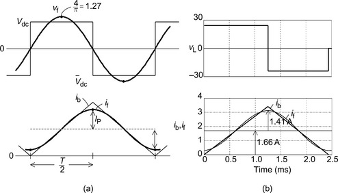
Figure 5.18 The maximum voltage and current: (a) ideal maximum voltage and current waveforms; (b) the maximum voltage and current in simulation
This equation is also written in terms of the current frequency f as
In the lower graph the current waveform ib, which is triangular in shape, is drawn. The sum of the dc and fundamental component if (having the peak amplitude of Ip) is also illustrated. The waveform shows the maximum current and (5.31) provides the voltage limitation line shown previously in Figure 5.17(a).
5.4.2 Acceleration test
It is quite important to investigate the influence of insufficient current from the current driver. In magnetic bearing applications the required amplitude and frequency of the current command increases as the rotational speed increases up to the critical speed. If the current command is outside the operating area then the radial positioning becomes unstable. Figure 5.19 shows a simulation of the rotational acceleration, including unbalance and sensor target eccentricity.
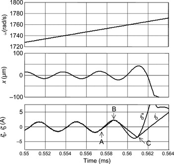
The current command and current are drawn in the bottom graph. The current follows the command up to point A; however, from point A to B, a discrepancy is seen. This is because enough voltage is not available to force the current to follow the command. Whilst they converge again at B, after B a significant error is seen. At point C the voltage is insufficient such that a fatal error is seen after point C, where the shaft radial position cannot be regulated and the shaft touches down to an emergency bearing. The required current peak is about 2 A at a frequency of 280 Hz. This limit corresponds to the case in Example 5.4. To avoid this problem, the following solutions can be implemented:
1. An increase in the dc voltage of the inverter.
2. A decrease in the number of series turns in the magnetic bearing winding to reduce the inductance. To compensate a reduction of series turns, parallel turns may be used with an increase in current rating.
3. The eccentric errors of the shaft, rotor and sensor target ring should be reduced and better mechanical balancing should be achieved.
4. The controller should be improved. The frequency characteristics of the radial position controller should be shaped so that current requirement is less. Feedforward signal injection may be considered.
5.5 Power devices and gate drive circuits
In this section, the characteristics of various power devices and gate driver circuits are described and waveform measurements are given. Insulated gate bipolar transistors and metal oxide silicon field effect transistors are discussed because these devices are popular. An example of a gate drive circuit is shown and the principles and operation are explained. In addition, the electrical failure mechanisms associated with the circuit are discussed and explained. The fundamental functions of a differential probe and isolators are introduced.
5.5.1 Power devices
Insulated gate bipolar transistors and metal oxide silicon field effect transistor are the most popular semiconductor devices used in inverters. Power transistors, which require considerable base current, have been used for over a decade. The IGBT is an improved power transistor with voltage controlled MOS gate characteristics. There are three terminals: gate, collector and emitter. Turn-on and turn-off is achieved by applying a specific voltage between the gate and emitter terminals. For example, if the gate terminal voltage is 15 V higher than the emitter terminal then the device conducts current from collector to emitter. If the gate–emitter voltage is zero or negative then the device is off. Note that the on-state and off-state are controlled by the voltage and, unlike in the power transistor, a high gate current is not required. Gate current injection is required only for a short period during turn-on to charge the gate capacitance. During turn-off, the charged energy is extracted. The required power for a gate drive circuit is much less than the equivalent base drive circuit for a power transistor and fast switching is obtained. However, IGBTs do have the good output characteristics of power transistors. The voltage and current ratings are available up to more than 1000V and 1000A. The on-state forward voltage drop is 1.6 to 3V. Hence IGBTs are preferred in applications of more than 100V.
Metal Oxide Silicon Field Effect Transistors have a longer history compared to IGBTs. The MOSFET has a fast switching speed and low on-state resistance. The three terminals are gate, drain and source. The drain and source correspond to the collector and emitter of the IGBT. The on-state voltage drop is a product of the drain-source resistance Ron and the drain current, so a low voltage drop is achieved with low Ron and low current. Hence MOSFETs are preferred in low voltage systems, e.g., 12, 24 and 48V applications.
5.5.2 Gate drive circuit
Figure 5.20 shows the structure of a main circuit with gate drive interface circuits. A digital processor provides the inverse logic ![]() and a logic power supply of 5V. When
and a logic power supply of 5V. When ![]() = 0, the main switches are on. In the gate drive circuits a photo coupler is driven by the current loop. The inverse logic with current loop provides a fail-safe logic for the off-state in power devices in a case of accidental wire disconnection.
= 0, the main switches are on. In the gate drive circuits a photo coupler is driven by the current loop. The inverse logic with current loop provides a fail-safe logic for the off-state in power devices in a case of accidental wire disconnection.
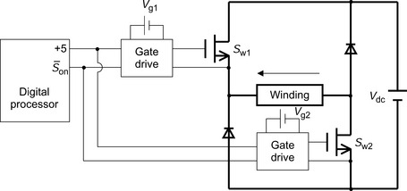
The gate drive circuits need isolated dc power supplies Vg1 and Vg2. Let us examine the negative voltage terminal potential of Vg1. The potential is equal to the source voltage of Sw1. If the winding voltage is positive then the negative terminal potential is equal to Vdc. If the winding voltage is negative then the negative terminal potential is zero. Hence the potential voltage has changed in accordance with winding voltage. Therefore Vg1 should be isolated using a transformer. In recent dc/dc converters the input dc power is converted to high frequency ac and applied to a primary winding in an integrated transformer to provide isolation. The output from the secondary winding of the transformer is rectified to obtain a dc voltage source. The use of a high frequency reduces the transformer size.
The isolation circuit also has frequency-dependent characteristics. In power devices, the switching speed is as fast as 0.5 μs where the slew rate is 600 V/μs for the case of Vdc = 300 V. Vg1 is supposed to maintain a constant voltage during this fast voltage transition so that excellent regulation at high frequency is required.
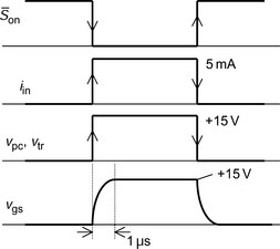
Figure 5.21 shows an example of a gate drive circuit and Figure 5.22 shows the operational waveforms. Twisted-pair wires are connected to the left side of the photo coupler, which has a high slew rate in common mode rejection ratio (CMRR) mode, for example 1000V/μs to avoid malfunction of the output stage. When ![]() = 0, current flows from the +5V supply and through the 1kΩ resistance and the photo diode. For the photo diode, there is an integrated circuit (IC) with a buffer that gives +15 V at the photo coupler output terminal. A complimentary transistor buffer amplifies the current; νtr has an amplitude of +15 and 0V with respect to the negative terminal of Vg1. This signal is the inverse of
= 0, current flows from the +5V supply and through the 1kΩ resistance and the photo diode. For the photo diode, there is an integrated circuit (IC) with a buffer that gives +15 V at the photo coupler output terminal. A complimentary transistor buffer amplifies the current; νtr has an amplitude of +15 and 0V with respect to the negative terminal of Vg1. This signal is the inverse of ![]() . The gate resistor Rg is to restrict the turn-on and turn-off speed of main switching devices. If the switching speed is too fast then turn-off delays in the diodes (integrated into the power devices) can cause inrush current. The gate resistor and gate capacitance provide an RC series circuit configuration so that the gate–source voltage waveform is delayed as shown in Figure 5.22.
. The gate resistor Rg is to restrict the turn-on and turn-off speed of main switching devices. If the switching speed is too fast then turn-off delays in the diodes (integrated into the power devices) can cause inrush current. The gate resistor and gate capacitance provide an RC series circuit configuration so that the gate–source voltage waveform is delayed as shown in Figure 5.22.

In power devices with low voltage and current ratings, the gate–source capacitance is rather low. In this case, the gate–source voltage can be directly driven by the photo coupler without an isolated dc power supply to reduce the cost.
The gate drive circuit may be replaced by capacitors using recently developed charge pump gate driver ICs.
5.5.3 Waveform checking and isolation
Single-phase inverters with a unidirectional current are not common for inverter circuits so that these power modules are not manufactured. Therefore these circuits have to be fabricated from components. The circuits may be tested by checking the waveforms. Incorrect waveform checking using an oscilloscope may cause a fatal electric breakdown in the inverter circuits. To avoid the problem let us see how the possible failure occurs when checking the waveform.
Figure 5.23(a,b) shows two possible two fault connections for an oscilloscope when attempting to see the voltage waveforms of the switching power devices. When we want to see if the power devices are working correctly, we look at the drain–source voltage of the two switching devices. Unfortunately, once the oscilloscope probes are connected as shown in Figure 5.23(a), the switching device Sw1 has a fatal inrush current because the source is connected to the bottom rail of the dc source via the oscilloscope. The inrush current occurs because the probe lead grounds are connected together by the oscilloscope channels and the internal impedance of Vdc is small so that the inrush current is extremely high. This will burn out the switching device and the probe leads.
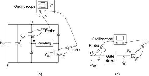
Figure 5.23 Possible typical failure: (a) failure caused by waveform checking; (b) failure caused by waveform checking
Figure 5.23(b) shows another possible connection of an oscilloscope. The on and off delay of the main switching device is being checked. Channel 1 is connected to the input terminals of gate drive circuit and channel 2 is connected to the main switching device. In this case, a failure may be avoided if isolation is provided. However, there are possible problems:
• If dc power supply of the digital processor is not isolated, Vdc is applied to ![]() , causing the digital processor circuit to break down.
, causing the digital processor circuit to break down.
• Even though the power supply is isolated, the output device of ![]() may break down because the output voltage is driven by the main circuit voltage.
may break down because the output voltage is driven by the main circuit voltage.
In order to avoid the problems associated with oscilloscope ground connections, differential probes or isolated amplifiers should be used. Differential probes allow the measured voltage to float and the ability to simply measure the potential difference between the probe terminals. Oscilloscope distributors supply this type of probes. An isolated amplifier is an alternative measurement method. A four-channel isolated amplifier provides a wide frequency range with less temperature drift of the offset voltage. Probes can be connected to the different voltage potentials and the output of the amplifier is connected to oscilloscope. For the cases in Figure 5.23 the inrush current and electric failure can be avoided by use of either of these two methods.