
I beseech your Lordships to be merciful to a broken reed.
Francis Bacon
CONETNS
11.1 Principles and Design of the Reed Switch
11.1.1 Pull-In Characteristics of a Reed Switch
11.1.2 Drop-Out Characteristics of a Reed Switch
11.1.3 Magnet Drive Characteristics of a Reed Switch
11.1.3.1 X-Y Characteristic H (Horizontal)
11.1.3.2 X-Z Characteristic H (Horizontal)
11.1.3.3 X-Y Characteristic V (Vertical)
11.2 Recommended Contact Plating
11.2.1 Materials for Contact Plating
11.2.5.5 Nitriding the Permalloy (Ni-Fe [48 wt%]) Blade Material
11.3 Contact Surface Degradation and Countermeasures
11.3.1 Surface Deactivation Treatment
11.3.1.1 Life Test of Samples Left for 24 Hours after Sealing
11.3.1.2 Life Test of Samples Left for One Week after Sealing
11.3.1.3 Life Test of Samples Left for One Month after Sealing
11.3.1.4 Life Test of Samples Left for Three Months, Six Months, and One Year after Sealing
11.3.2 Prevention of Contact Adhesion
11.4 Applications of Reed Switches
11.4.2 Applications of Magnetic-Driven Reed Switches
11.1 Principles and Design of the Reed Switch
A reed switch is a pair of blades in a magnetic material, such as 52-alloy (Ni 52%, Fe Bal.), sealed in a glass tube together with an inert gas (see Figure 11.1) [1,2,3,4,5]. As shown in Figure 11.2, the magnetic field of a coil or magnet induces a north or south pole in a blade, and consequently the contacts make as a result of the attractive force. When the magnetic field is removed, the contacts break as a result of the elasticity in the reeds.
A reed switch has the following characteristics:
1. Since the contacts, together with an inert gas, are hermetically sealed in a glass tube, the substitution operation is free from the influence of the external environment.
2. Since a reed switch undergoes no unnecessary operations because it has few mechanically moving parts, the life with no load is virtually limitless.
3. Since the moving components are lightweight with a high resonant frequency, the contacts make or break very quickly.
11.1.1 Pull-In Characteristics of a Reed Switch
The relationship between Φg (the magnetic flux passing through a contact gap) and Q (magnetomotive force Q when the blades are set along the axis of the coil with a certain contact gap and overlap) in Figure 11.3 [5,6,7,8,9,10,11,12] is represented by
Φg=QrL1cosh αL2/2−cosh α(L2−L1)/2cosh αL2/2+(prg/2α)sinh αL2/2 |
(11.1) |
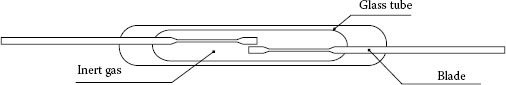
FIGURE 11.1
Basic structure of reed switch.
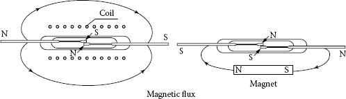
FIGURE 11.2
Principle of operating reed switch.
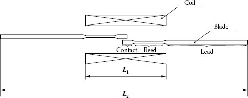
FIGURE 11.3
Magnetic analysis model of reed switch.
where, Φg = magnetic flux passing through the contact gap, Q = magnetomotive force, L1 = coil length, L2 = reed switch length, p = permeance per unit length, r = magnetic resistance per unit length, rg = magnetic resistance per unit length of contact, α =√pr
With a magnetomotive force per unit length taken as q, the number of coil turns as N, and coil current as I in Equation 11.1, the following expression holds:
(11.2) |
Then, NI is represented by Equation 11.3 below, on rearranging Equation 11.1:
NI=L1rcosh αL2/2+(prg/2α)sinh αL2/2cosh αL2/2−cosh α(L2−L1)/2Φg |
(11.3) |
The permeance per unit length, p, is approximated by the permeance when an elongated ellipsoid of rotation symmetry is magnetized in the direction of the length:
(11.4) |
Nd=1ε2−1(ε√ε2−1ln(ε+√ε2−1)−1) |
(11.5) |
(11.6) |
Where, Nd = demagnetizing factor, d = lead diameter, μ0 = magnetic susceptibility in vacuum (4π × 10−7 H/m in the MKS system of units, 1 in the CGS system of units)
With the magnetic susceptibility taken as μ, r is represented by
(11.7) |
With the permeance of contact taken as pg, rg is represented by
(11.8) |
Next we will obtain pg. Using the dimensions of the contact as shown in Figure 11.4. Where, g = contact gap, a = overlap, w1 = contact width and t1 = contact thickness. The permeance of contact, pg, is the sum of the permeance of the side, pgs, and the permeance of the facing surface, pgt, and is as follows:
(11.9) |
(11.10) |
k, as a function of g/a with tl/wl as a parameter, is obtained from Figure 11.5. From Equations 11.8 through 11.10, rg is expressed by
(11.11) |
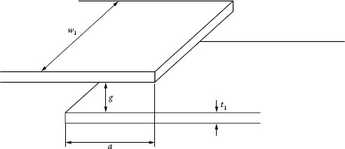
FIGURE 11.4
Dimensions of contact.
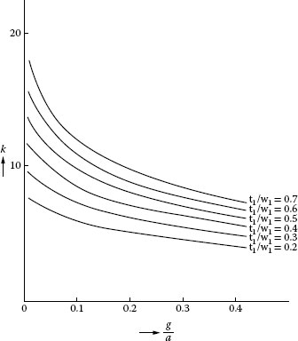
FIGURE 11.5
k vs. ga
The magnetic attractive force acting on the blades, Fm, is expressed by
(11.12) |
Applying Equation 11.11 gives
(11.13) |
where μ0 = 1. When a reed switch is closed, g = 0. The magnetic attractive force in this case, F0, is expressed by
(11.14) |
where the contacts are assumed to be not plated. If a reed switch, whose contacts are plated to a thickness of tp, is closed by a saturated magnetic flux Φs caused by a soak current, magnetic attractive force Fs is expressed, from Equation 11.13, as follows:
(11.15) |
Equation 11.15 expresses a magnetic attractive force for an ordinary operation. With the stiffness of a reed, indicating the spring strength of the reed, taken as S, the retractive force in the blades, Fr, is expressed by
(11.16) |
where x = displacement. With a contact gap when the reed switch is open taken as G, the retractive force for contact gap g is expressed by
(11.17) |
From Equations 11.13 and 11.14, magnetic attractive force Fm is expressed by
(11.18) |
Figure 11.6 shows the relationship between a retractive force expressed by Equation 11.17 and a magnetic attractive force expressed by Equation 11.18. The abscissa represents a contact gap g, and the ordinate, magnetic attractive force Fm and retractive force Fr.
The straight line represents Equation 11.17 and is called a load line. The three curves represent Equation 11.18 and are called attractive force curves. The difference between them is caused by F0. Each of them is described below.
Fm1
However, when g<g1,Fm1<Fr
Consequently, the reed switch cannot close, and the apparent gap becomes g1 only.
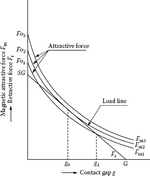
FIGURE 11.6
Attractive and retractive characteristics.
Fm2
When g<g0,Fm2>Fr
Consequently, the reed switch closes.
F02: The point at which the attractive force curve touches the load line is the attractive force required to pull the reed switch. The magnetic flux at this time is pull-in magnetic flux ΦPI. In general, contact force Fc is expressed by
(11.19) |
And contact force Fc2
(11.20) |
This represents the contact force when the contacts pull in.
Fm3
Consequently, the reed switch is always closed.
Contact force Fc3
(11.21) |
Applying Equation 11.15 to F03
(11.22) |
This represents a contact force during ordinary operation.
We will now obtain the pull-in conditions for a reed switch. A reed switch pulls in at the point where the attractive force curve touches the load line. At this point, with a contact gap of g0, the retractive force expressed by Equation 11.17 becomes equal to the magnetic attractive force expressed by Equation 11.18. Therefore,
(11.23) |
Then
(11.24) |
Since the attractive force touches the load line, the slopes become identical as expressed below:
(11.25) |
Then
(11.26) |
From Equations 11.24 and 11.26,
(11.27) |
Substituting pull-in ampere-turns NIPI for NI and pull-in magnetic flux ΦPI for Φg in Equation 11.3, and using
1 ampere turn (AT)=4π10 gilbert |
(11.28) |
gives
NIPI=104πL1rcosh αL2/2+(prg/2α)sinh αL2/2cosh αL2/2−cosh α(L2−L1)/2ΦPI(AT) |
(11.29) |
A reed switch whose contact gap is G when it breaks begins to close at a contact gap of g0. Then, magnetic resistance rg of the contact is obtained from Equation 11.11 as follows:
(11.30) |
where μ0 = 1.
ΦPI is expressed from Equations 11.26 and 11.27 as follows:
ΦPI=√4(1+kGa)327k1aS×8πaw1×980 |
(11.31) |
Now, if the dimensions of a reed switch are given, the NI-Φ characteristics of the switch can be obtained. However, it is necessary to calculate the stiffness S of the reed in advance.
To calculate the stiffness S of a reed, specify the dimensions of the reed, apply load W(g), and take the deflection of the reed as x (mm) as shown in Figure 11.7.
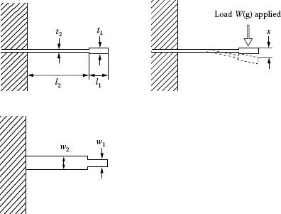
FIGURE 11.7
Dimensions of reed.
With cross-sectional secondary moments taken as I1 and I2, the stiffness S of a stepped cantilever as shown in Figure 11.7 is calculated by
S=Wx =Eℓ313I1+ℓ323I2+1I2(ℓ21ℓ2+ℓ1ℓ22) |
(11.32) |
(11.33) |
(11.34) |
where E is Young’s modulus. Young’s modulus of 52-alloy annealed at 850°C in a hydrogen atmosphere for 10 minutes is as follows:
(11.35) |
Obtaining magnetic resistance r requires the magnetic susceptibility in Equation 11.7. μ is determined by magnetic flux Φ.
If the diameter, d, of wire to be used as a blade in this reed switch is 0.5 mm, it is necessary to obtain the B–H characteristics of a 0.5 mm diameter wire. Using the B and H values obtained with a B–H curve tracer, the magnetic flux Φ and magnetic susceptibility μ can be obtained from
(11.36) |
(11.37) |
Table 11.1 gives Φ and μ values obtained from the measured B–H characteristics of a 40 mm diameter ring made of a 0.5 mm diameter 52-alloy wire annealed at 850°C in a hydrogen atmosphere for 10 minutes. Figure 11.8a shows the Φ–μ curve.
From Equations 11.29 through 11.31, the relationship between contact gap G, overlap a, and pull-in value NIPI is as shown in Figure 11.8b. In addition to the fact that the pull-in value increases as the contact gap increases (see Figure 11.6), Figure 11.8b shows the value of am at which NIPI is minimized by overlap being changed with the contact gap kept constant. As the contact gap increases, am decreases. The variations in NIPI in the manufacturing of reed switches can be made smaller by using am in the reed switch design stage.
11.1.2 Drop-Out Characteristics of a Reed Switch
We will now obtain drop-out ampere-turns NIDO of a reed switch using blades whose contact plating thickness is tp. Substituting NIDO for NI, ΦDO for Φg, and rp for rg because of the contact plating in Equation 11.3, and using Equation 11.28, gives
NIDO=104πL1rcosh αL2/2+(prp/2α)sinh αL2/2cosh αL2/2−cosh α(L2−L1)/2ΦDO(AT) |
(11.38) |
TABLE 11.1
Magnetic Characteristics of 0.5 mm Diameter 52-Alloy Wire
H (Oersted) |
B (Gauss) |
Φ (Maxwell) |
μ |
0.10 |
291 |
0.57 |
2,910 |
0.15 |
523 |
1.03 |
3,487 |
0.20 |
1,168 |
2.29 |
5,840 |
0.25 |
1,915 |
3.76 |
7,660 |
0.30 |
2,555 |
5.02 |
8,517 |
0.35 |
3,830 |
7.52 |
10,943 |
0.40 |
5,910 |
11.60 |
14,775 |
0.45 |
7,025 |
13.79 |
15,611 |
0.50 |
7,820 |
15.35 |
15,640 |
0.55 |
8,460 |
16.61 |
15,382 |
0.60 |
8,630 |
16.94 |
14,383 |
1.1 |
10,540 |
20.70 |
10,540 |
2.0 |
11,650 |
22.87 |
5,825 |
2.5 |
11,970 |
23.50 |
4,788 |
3.0 |
12,440 |
24.43 |
4,147 |
5.0 |
13,250 |
26.02 |
2,650 |
10.0 |
14,200 |
27.88 |
1,420 |

FIGURE 11.8
(a) Φ–μ curve of 0.5 mm diameter 52 alloy wire. (b) Relationship between pull-in value, contact gap, and overlap.
Magnetic attractive force Fm, as in Equation 11.15, is as follows:
(11.39) |
Retractive force Fr is expressed by
(11.40) |
Then, drop-out magnetic flux ΦDO is expressed by
ΦDO=√8π(1+k2tpa)2aw1×980×S(G−2tp) |
(11.41) |
From Equation 11.11,
(11.42) |
In this case, μ0 = 1.
It is obvious from Figure 11.6 that the drop-out value increases as the contact gap increases. Figure 11.9 shows the change in drop-out value NIDO with overlap a and contact plating thickness tp for a constant contact gap of G. Figure 11.9 shows that the drop-out value increases as the contact plating thickness or overlap increases.
11.1.3 Magnet Drive Characteristics of a Reed Switch
As mentioned previously, one of the characteristics of the reed switch is that it can be easily driven by an external magnet as well as a coil. There are many kinds of magnets, and there are also many different magnet shapes and magnetizing methods. There are also many kinds of reed switches with different pull-in values. As a result, the magnet drive characteristics becomes complicated. This section explains typical magnet drive characteristics [5].
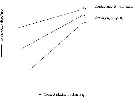
FIGURE 11.9
Relationship between drop-out value, contact plating thickness, and overlap.
11.1.3.1 X–Y Characteristic H (Horizontal)
Here a rectangular bar magnet is used with the magnet movement direction and the center of the reed switch to Z = 0 (constant) as shown in Figure 11.10a. The X–Y characteristic H is the magnetic drive characteristic of the reed switch when the magnet moves freely in the X–Y plane with the pole direction kept parallel to the reed switch. The reed switch closes and opens as the magnet moves. The “on” point is taken as the point where the reed switch closes due to the movement of the magnet, and the “off” point as the point where the closed reed switch opens due to the movement of the magnet. Plotting the “on” and “off” points results in Figure 11.10b, i.e., X–Y characteristic H. In Figure 11.10b, the area inside the solid line connecting the “on” points is called the “on” area, and the area outside the broken line connecting the “off” points is called the “off” area. The area between the “on” area and the “off” area is called the “hold” area, “hysteresis” area, or “differential” area. When the intensity of the magnet is strong, the “on” area and “hold” area marked by *are generated, resulting in three-point operation.
11.1.3.2 X–Z Characteristic H (Horizontal)
Here the magnet movement direction is shown in Figure 11.11a. The X–Z characteristic H is the magnetic drive characteristic of the reed switch when the magnet moves freely in the X–Z plane with the pole direction kept parallel to the reed switch. Connecting the on and off points, as in the case of X–Y characteristic H, results in X–Z characteristic H as shown in Figure 11.11b.
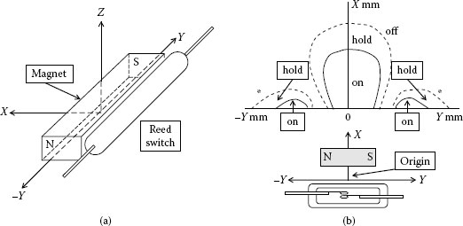
FIGURE 11.10
(a) Magnet movement direction (#1). (b) X–Y characteristic H.
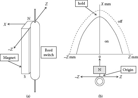
FIGURE 11.11
(a) Magnet movement direction (#2). (b) X–Z characteristic H.
11.1.3.3 X–Y Characteristic V (Vertical)
Here the magnet movement direction with the center of the reed switch to Z = 0 (constant) is shown in Figure 11.12a. The X–Y characteristic V is the magnet drive characteristic of the reed switch when the magnet moves freely in the X–Y plane with the pole direction kept perpendicular to the reed switch. Connecting the on and off points, as in the case of the X–Y characteristic H and X–Z characteristic H, results in X–Y characteristic V as shown in Figure 11.12b. In the X–Y characteristic V, the reed switch opens when the magnet comes near the contacts of the reed switch.
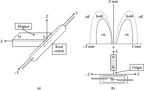
FIGURE 11.12
(a) Magnet movement direction (III). (b) X–Y characteristic V.
11.2 Recommended Contact Plating
Contact plating as well as sealing is the most important process in the manufacture of reed switches. The quality of contact plating determines the contact characteristics of the reed switch. This section describes materials for contact plating in detail [5].
11.2.1 Materials for Contact Plating
In ordinary reed switches, except for some changeover-type reed switches, which use a special plating, gold is plated onto 52-alloy as a ground layer, and rhodium or ruthenium in some cases is plated on the background layer.
Gold is usually plated as a ground layer. There are two kinds of gold-plating solutions: pure gold and cyanic. The pure gold type is in popular use. Gold striking is performed before gold plating in many instances. Gold striking may be necessary to attain secure adhesion. If the required adhesion and other characteristics can be attained by gold plating only, gold striking can be omitted.
Palladium has been attracting attention as an alternative to gold. Palladium-plating solution of good quality is also being developed. Since the density of palladium is about 60% that of gold, the weight of palladium used is about 40% less than that of gold plating for the same plating thickness. However, the monetary value of palladium is now similar to that of gold. Consequently, the cost of using it for ground plating cannot really be shortened. Palladium is somewhat advantageous in terms of performance because of higher melting point and hardness twice that of gold. Table 11.2 lists the properties of gold and palladium.
TABLE 11.2
Properties of Gold and Palladium
Gold |
Palladium |
|
Atomic number |
79 |
46 |
Atomic weight |
197.0 |
106.4 |
Density (20°C) |
19.3 g/cm3 |
2.03 g/cm3 |
Crystalline structure |
Face-centered cubic lattice |
Face-centered cubic lattice |
Melting point |
1,063°C |
1,555°C |
Hardness |
2.5~3 |
4.8 |
Specific resistance |
2.2 μΩ cm (18°C) |
10.4 μΩ cm |
Rhodium is a commonly used contact material for reed switches. Rhodium has a high melting point and hardness, and has excellent abrasion resistance, resistance against sticking, and corrosion resistance.
Initially when rhodium was first put on the market, a good plating solution was not available, and the rhodium contact surface had a problem of cracking. The cracking problem was addressed over 25 years ago and successful crack-free rhodium plating with thicknesses up to 10 μm was achieved. This success was achieved partly by the development of an excellent stress relaxing agent. This technique, together with the surface deactivation treatment described in Section 11.3.1, are core techniques for the development of reed switches’ rhodium contact. Since thick plating is possible with these techniques, reed switches with wide variations, ranging from ultra-miniature reed switches employing thin plating to high-power reed switches employing thick plating, can be obtained. A proper pretreatment and post-treatment make almost maintenance-free and stable rhodium plating possible.
At present, the matter primary concerning rhodium is cost. Limited supplies of rhodium are produced and it is used as a catalyst in anti-pollution equipment. As a result, the price has risen. Good contact plating requires that the concentration of sulfuric acid in the rhodium-plating solution to be maintained below a certain point, then it is often necessary to replace the rhodium-plating solution. This also raises the cost. Research is being conducted into removing only the sulfuric acid from the rhodium-plating solution. A sulfuric acid removing system, however, has not been completed yet due to a filtration problem and other problems. In order to alleviate the cost problem, ruthenium is an attractive alternative to rhodium.
The atomic number of ruthenium is 44, adjacent to rhodium, with an atomic number of 45, in the periodic table. Ruthenium has a higher melting point and hardness and better abrasion resistance, resistance against sticking, and corrosion resistance than rhodium. Although the production of ruthenium is lower than that of rhodium, its price remains relatively low, because it is unfit for ornamentation, i.e., a poor gloss results from its low reflectance of visible light rays.
The problem of cracking in plated layers is again a grievous one. An effective stress-relaxing agent has not been developed for ruthenium in spite of the past research for a solution. Even if the plating conditions are optimized and post-treatment is executed properly, the maximum crack-free plating thickness is about 1.5 μm. Research continues on special post-plating treatments to control cracking. Some manufacturers perform crack-free plating of ruthenium by sputtering, not by electroplating. Sputtering, however, has its own problems of productivity and quality.
Thin plating of ruthenium has a life several times that of rhodium at low and intermediate loads. In this connection, the market potential associated with these loads, mainly applications for reed relays for use in ATEs (LSI testers and board tester), will probably increase.
It is said that ruthenium does not require the surface deactivation treatment (See Section 11.3.1) after plating because a thin, stable oxide film is formed on the plated surface. There are many areas to be analyzed and studied concerning ruthenium plated surfaces [13,14].
Many attempts have been made to increase the plating thickness of ruthenium. One of them is alloy plating which uses rhodium containing about 10% ruthenium. Plating solution for this alloy plating is on the market. Ruthenium-silver alloy plating has also been reported.
Table 11.3 gives the properties of rhodium and ruthenium.
In addition to the above-mentioned plating, copper plating, nickel plating, tungsten plating, titanium, and iridium plating are actually practiced or have been reported. Some of these are described below.
A non-magnetic chip is welded to the normally closed blade of a changeover-type reed switch. Copper-plating (0.33 mm thick) can also be used in place of the non-magnetic chip, see Figure 11.13. The plating a thickness of copper that exceeds 100 μm is quite complex. It involves the optimum selection of copper–plating solution, diffusion treatment and frequent gold strikings, but stable contact characteristics can be obtained. In the early stages, the copper–plated portion can cause problems that result from the heat in surface treatment and sealing. However, this non-magnetization process is free of problems and provides quite stable non-magnetization.
TABLE 11.3
Properties of Rhodium and Ruthenium
Rhodium |
Ruthenium |
|
Atomic number |
45 |
44 |
Atomic weight |
102.9 |
101.1 |
Density |
12.41 g/cm3 (20°C) |
12.30 g/cm3(19°C) |
Crystalline structure |
Face-centered cubic lattice |
Hexagonal close-packed lattice |
Melting point |
1,966°C |
2,350°C |
Hardness (plated) |
6 |
6.5 |
Specific resistance (plated) |
5.1 μΩ cm (20°C) |
7.46 μΩ cm |
Mean reflectance of visible rays |
79% |
635 |
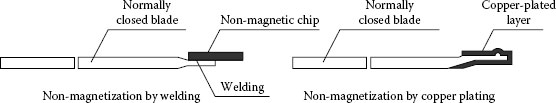
FIGURE 11.13
Non-magnetization of normally closed blade.
Tungsten, whose melting point is much higher than that of rhodium and ruthenium, is a very useful contact material for high-power reed switches for which the user’s requirements are getting more severe [15]. Tungsten is usually plated on a contact by chemical vapor deposition (CVD), which is quite costly. It has been confirmed that a tungsten layer shows excellent abrasion resistance and resistance against sticking because of the exceptionally high melting point. The tungsten layer, however, soon oxidizes in air, and consequently the initial contact resistance can be high. This problem can be solved by surface treatment after CVD and by optimizing the sealing gas.
Rhenium, like tungsten, has a higher melting point than both rhodium and ruthenium, and is one of the quite useful contact materials for high-power reed switches. Reported is a reed switch whose contact surface is covered with a three-layer structure of Re–Au–Re to suppress metal transfer caused by a molten metal bridge when the contacts begin to open.
Iridium also has a higher melting point that rhodium and ruthenium, a resistivity close to that of rhodium and hardness close to that of ruthenium. Successful crack free contact surfaces have been obtained by using a gold substrate on the blade, a rhodium plate on the gold and a final iridium plate on the rhodium. Testing using inductive circuits of 24 V dc, 36 mA and 12 V dc, 73 mA show a superior performance over rhodium contacts [16].
11.2.5.5 Nitriding the Permalloy (Ni-Fe [48 wt%]) Blade Material
An interesting study of nitriding the Ni-Fe blade instead of electroplating it with a contact material shows that this modification of the blade can perform satisfactorily for some applications of the reed switch [17].
11.3 Contact Surface Degradation and Countermeasures
Reed switches have a very simple structure and very small size. Coupled with the developments in electronics, reed switches have greatly advanced in terms of function and performance. Two of these advances are discussed in this section.
11.3.1 Surface Deactivation Treatment
The invention of the surface deactivation treatment and introduction of this technique into reed switch production are very significant in the history of reed switches. The surface deactivation treatment is one of the main techniques for reed switches using rhodium contacts.
The background to the invention of the surface deactivation treatment is the phenomenon that when a rhodium contact reed switch is operated at a low load, the contact resistance increases during the initial stage of operations [18]. Figure 11.14 shows this phenomenon. Examination of the contact surface of a reed switch whose contact resistance had increased reveals the formation of brown insulating material. Analysis by electron probe microanalysis (EPMA) shows that the material is carbon (see Figure 11.15a and b). Rhodium is active in adsorption and catalysis. Plated rhodium on a contact surface adsorbs organic impurities from the air, and the mechanical energy generated by the collisions of contacts polymerizes them. The contact resistance seems to decrease and converge to a certain level after increasing, because the generated polymer is destroyed and polymer pieces scatter. Since the polymer pieces are present between contacts, the contact resistance is unstable (see Figure 11.16a and b).
In order to prevent this polymerization, the rhodium-plated surface must be deactivated to suppress the adsorbing and catalytic activities. The deactivation process requires the blades be treated at 450°C in an oxygen environment. Organic impurities adsorbed on the blade contact surface are removed by burning, and then an oxygen film is formed on the cleaned rhodium surface to prevent organic impurities from being adsorbed again [19] (patent no. 916386 in Japan, patent no. 3857175 in USA, patent no. 2303587 in West Germany).
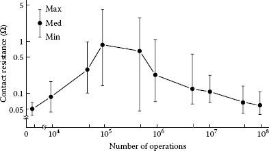
FIGURE 11.14
Increase in contact resistance of rhodium contact reed switch.
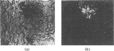
FIGURE 11.15
(a) Contact surface of reed switch after 105 operation (× 550); (b) X-ray image of contact surface of reed switch after 105 operations (× 550).
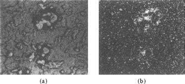
FIGURE 11.16
(a) Contact surface of reed switch after 107 operations (× 550); (b) X-ray image of contact surface of reed switch after 107 operations (× 550).
TABLE 11.4
Samples for Checking the Effect of the Surface Deactivation Treatment
|
|
Surface Deactivation Treatment |
|
Left in benzene vapor |
|
No |
Yes |
|
No |
Rh |
Rh + O2 |
|
Yes |
Rh + benzene |
Rh + O2 + benzine |
To evaluate the effect of the surface deactivation treatment, samples as shown in Table 11.4 were prepared. Samples which had been left in benzene vapor for 24 hours were also used. Some of these samples were left for 24 hours after sealing, some for one week, some for one month, some for three months, some for six months, and some for one year. Then, individual groups underwent a life test of 100 million operations with a resistive load of 12 V/5 mA operated by a permanent magnet.
11.3.1.1 Life Test of Samples Left for 24 Hours after Sealing
As shown in Figure 11.17a, the “Rh + O2” group, i.e. the deactivated contact surface group, had a stable contact resistance throughout 100 million operations, indicating that no polymer was formed. The “Rh + O2 + benzene” group also had a stable contact resistance even though the group was left in benzene vapor for 24 hours after the surface deactivation treatment. On the other hand, the “Rh” group, i.e., a group without the surface deactivation treatment, had an increase in contact resistance, indicating the formation of polymer. In particular, the “Rh + benzene” group, i.e., a group that did not receive the surface deactivation treatment and that was left for 24 hours in benzene vapor, had an extreme increase in contact resistance, indicating the formation of a lot of polymer (see Figure 11.18a and b). For the other samples, only the “Rh” and “Rh + O2” groups underwent a test.
11.3.1.2 Life Test of Samples Left for One Week after Sealing
The “Rh + O2” group had a stable contact resistance throughout 100 million operations. However, the “Rh” group had a larger increase in contact resistance than the group left for 24 hours, and the variation in contact resistance was also larger (see Figure 11.17b).
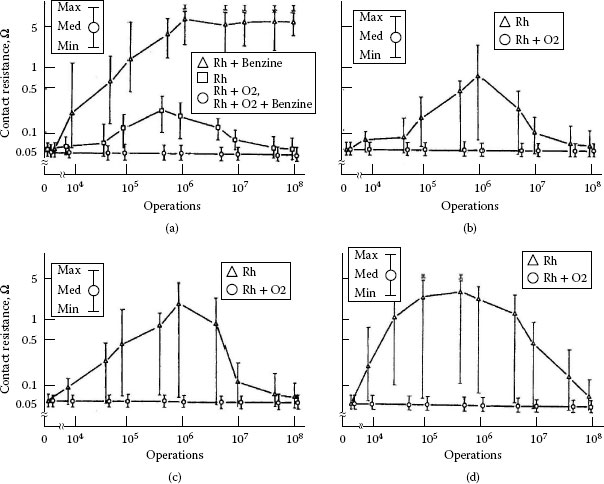
FIGURE 11.17
(a) Fluctuations in contact resistance (life test of samples left for 24 hours after sealing); (b) fluctuations in contact resistance (life test of samples left for one week after sealing); (c) fluctuations in contact resistance (life test of samples left for one month after sealing); (d) fluctuations in contact resistance (life test of samples left for one year after sealing).
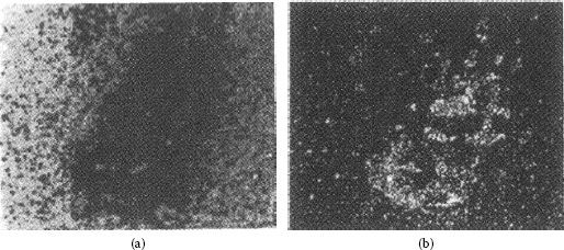
FIGURE 11.18
(a) Contact surface of reed switch after 105 operations (left in benzene vapor without the surface deactivation treatment); (b) X-ray image of contact surface of reed switch after 105 operations (left in benzene vapor without the surface deactivation treatment).
11.3.1.3 Life Test of Samples Left for One Month after Sealing
The “Rh + O2” group had a stable contact resistance. The “Rh” group had a larger increase in contact resistance than the group left for one week (see Figure 11.17c).
11.3.1.4 Life Test of Samples Left for Three Months, Six Months, and One Year after Sealing
The data were similar to the one year data shown in Figure 11.17d, the “Rh” group experienced a further increase in contact resistance. The “Rh + O2” group had as stable a contact resistance as the group left for 24 hours, and the formation of polymer was not mentioned in this group (see Figure 11.19).
These experiments show that a surface deactivation treatment suppresses adsorbing and catalytic activities. As rhodium generally resists oxidation, then studies of on how oxygen exists on the rhodium-plated contact surface were made [20,21,22]. The relationship between the contact surface treatment temperature and amount of oxygen on the contact surface was examined using Auger electron spectroscopy (AES) [23]. Figure 11.20 shows the results. Before the contacts were sealed, the amount of oxygen on the rhodium surface simply increases with the treatment temperature. However, after the contacts were sealed, the amount of oxygen increased sharply at a treatment temperature of 400°C–450°C, but the amount was almost constant at very low levels at a treatment temperature of below 400°C. This meant that virtually all oxygen on the rhodium surface treated at below 400°C dissociated. Since the temperature range of 400°C–450°C seemed to be important for the establishment of an oxygen layer on the rhodium surface, further tests were conducted using reflection high-energy electron diffraction (RHEED), molecular optical laser examiner (MOLE) [24], and X-ray photoelectron spectroscopy (XPS) [25, 26]. The RHEED electron diffraction patterns showed that rhodium oxide was not detected on the rhodium surface without deactivation treatment and the rhodium surface treated at 300°C. However, a thin broad electron diffraction pattern of rhodium oxide (Rh2O3) was obtained from the rhodium surface treated at 400°C, and a clear electron diffraction pattern of Rh2O3 was obtained from the rhodium surface treated at 450°C. In addition, a further intensive electron diffraction pattern of Rh2O3 was obtained from the rhodium surface treated at 500°C. In other words, rhodium oxide (Rh3O3) with less crystallization started to emerge on the rhodium surface treated at 400°C, and Rh2O3 with increased crystallization existed stably on the rhodium surface treated at 450°C. A change in Rh2O3 on the rhodium surface in a temperature range of 400°C–450°C corresponded to the critical temperature zone in AES. More Rh2O3 seems to exist on the rhodium surface treated at 500°C. The Raman band of Rh2O3 was not observed from the untreated rhodium surface and the rhodium surface treated at 400°C, but the Raman band of Rh2O3 was observed from the rhodium surface treated at 450°C. In addition, a more intensive Raman band of Rh2O3 was observed from the rhodium surface treated at 500°C. The above analytic results showed that an Rh2O3 film existed on the rhodium surface treated at 450°C and a thicker Rh2O3 film was formed by treatment at 500°C. The existence of Rh2O3 film at a treatment temperature of 450°C, but not at 400°C corresponded to the critical temperature zone in the AES. Table 11.5 shows the binding energy of and difference between the Rh3d5/2
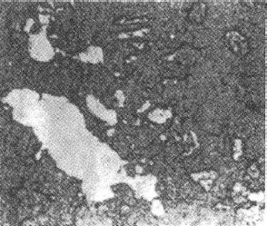
FIGURE 11.19
Non-magnetization of normally closed blade.
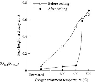
FIGURE 11.20
Amount of oxygen on rhodium surface vs. treatment temperature.
TABLE 11.5
Binding Energy of Rh3d5/2
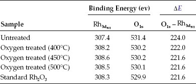
The results of the analysis above show that metal rhodium accounts for most of the untreated rhodium surface, but the rhodium oxide (Rh2O3) begins to be generated in the rhodium surface treated at 400°C and coexists with metallic rhodium. Only Rh2O3 is observed on the rhodium surface treated at 450°C, and the rhodium surface treated at 500°C is the same as that treated at 450°C. A change from the coexistence of Rh and Rh2O3 on the rhodium surface treated at 400°C to the existence of Rh2O3 only on the rhodium surface treated at 450°C corresponds to the critical temperature zone in AES. The RHEED, MOLE, and XPS, indeed confirm that oxygen exists on the deactivated rhodium-plated contact surface in the form of rhodium oxide (Rh2O3). Contact surface deactivation also improves the sealing properties through a betterment in the usability of blades. In other words, a metal surface covered with an oxide film shows better adhesion to glass than a pure metal surface. This is because metal oxide diffuses into the glass and promotes a bond between the glass and metal in sealing.
11.3.2 Prevention of Contact Adhesion
Adhesion of contacts that is called soft sticking of the contacts is caused by a friction of contact surfaces. Soft sticking has a low detection rate and is difficult to reproduce in distinction from ordinary sticking in which a load current and discharge make the contact surfaces rugged by erosion and the rugged contact surfaces stick to each other. Since it is difficult to predict when soft sticking occurs, soft sticking used to be one of the critical factors reducing the reliability of reed switches. Thus, the study of soft sticking is one of critical interest. Oxygen on the rhodium-plated contact is effective against soft sticking and has been used to suppress soft sticking [27,28,29,30].
Blades were prepared whose rhodium-plated contacts were deactivated and blades whose rhodium-plated contacts were left untreated. They were sealed in glass tubes in a nitrogen atmosphere or a highly reducing atmosphere including hydrogen (see Table 11.6). Figure 11.21a shows the sticking test circuit, and Figure 11.21b shows the sticking test mode. Adhesion was checked after every reed switch operation. In Figure 11.21b, coil excitation was attained by half-wave rectification of 50 Hz ac and the peak was 70 ampere turns (AT). A load of 50 kΩ (5 V and 100 μA) was connected to the contacts.
Figure 11.22a shows the results of the sticking test. Sticking occurred with reed switches whose contacts were deactivated and locked in a hydrogen environment and reed switches whose contacts were untreated and sealed in a nitrogen or hydrogen atmosphere. The sticking occurrence rate was roughly the same in these cases. No sticking at all was detected with reed switches whose contacts were deactivated and locked in a nitrogen atmosphere. The oxygen amount on the contact surface was analyzed of each sample using Auger electron spectroscopy (AES) to define the relationship between the outcomes of the sticking test and oxygen along the touch surface. Figure 11.22b shows the results of the analysis. Virtually no oxygen exists on the contact surface of reed switches whose contacts were deactivated and locked in a hydrogen atmosphere: the hydrogen atmosphere effectively reduced the oxygen. The reed switches whose contacts were untreated and sealed in a nitrogen or hydrogen atmosphere also showed no oxygen on the contact surfaces. There was, however, a lot of oxygen on the contact surface of reed switches whose contacts were deactivated and sealed in a nitrogen atmosphere in the form of Rh2O3 (see Section 11.3.1) Thus, only those reed switches free from sticking are those whose contacts are deactivated and sealed in a nitrogen atmosphere. Because there is a lot of oxygen on the contact surfaces of these switches, it can be deduced that oxygen on the rhodium-plated contact surface not only results in a stable contact resistance, but also is effective against contact sticking.
O2N2 |
Contact surface deactivated, sealed in N2 atmosphere |
O2H2 |
Contact surface deactivated, sealed in H2 atmosphere |
N2 |
Untreated, sealed in N2 atmosphere |
H2 |
Untreated, sealed in H2 atmosphere |
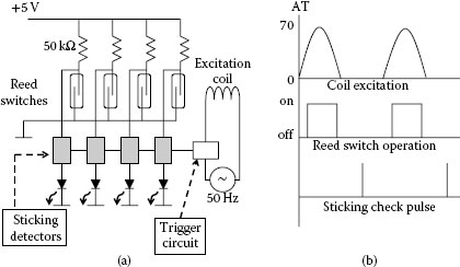
FIGURE 11.21
(a) Sticking test circuit. (b) Sticking test mode.
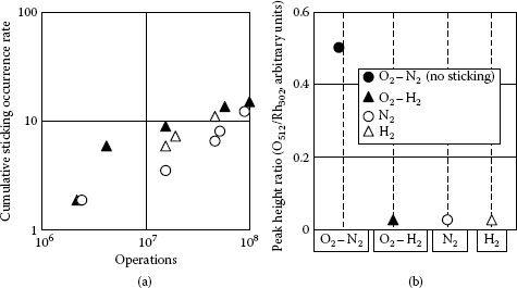
FIGURE 11.22
(a) Results of sticking test. (b) Amount of oxygen on contact surface.
11.4 Applications of Reed Switches
Reed switches have been used as reed relays-reed switches with multilayer coils around their glass tubes—in many cases since their development. They have also been used, in combination with permanent magnets, with various devices and equipment. At present, many kinds of reed relays have been developed, and also diversified requirements have expanded the applications of magnet-driven reed switches [5,6]. Reed switches can also be used as thermal switches, which go on and off according to the temperature, by using thermal ferrite.
A reed relay is an electromagnetic relay consisting of a reed switch and a driving coil around it or by using a permanent magnet as shown in Figures 11.2 and 11.3. The driving coil or magnet activates switching. There are many kinds of reed relays according to what they are to be applied for. Reed relays have the features described below.
1. They have excellent resistance to environment. Since the contacts are hermetically sealed in a glass tube, they are free from the influence of the surrounding atmosphere. An explosion-proof structure is employed.
2. They have excellent operating characteristics. The operating time, bounce time, and release time are short (see Figure 11.23). Although they vary, depending on the model, the operate time and bounce time are 0.5 ms maximum and the departure time is 0.2 ms maximum [31]. These are one tenth or less than those for mechanical relays.
3. Their input and output are completely isolated from each other electrically.
4. They are miniature and lightweight. The trend of reducing the size of devices and equipment causes reed relays to be miniaturized further. This trend is particularly noticeable with reed relays in ATEs (LSI testers and board testers), which use many reed relays. At present, miniature reed relays measure only 15 mm × 5 mm × 5 mm.
5. They have high sensitivity. Reed relays can control a large current and large voltage on the output side with a small input current of several to several tens of milliamperes.
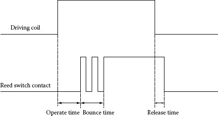
FIGURE 11.23
Operating characteristics of reed relay.
Various types of reed relays using these features have been developed along with the development of office automation (OA), factory automation (FA), and home automation (HA). Specifically speaking, they are SIP-type reed relays and DIP-type reed relays which are easily automatically mounted on printed circuit boards and can be directly driven by TTL-ICs and CMOS-ICs, surface-mounted-type reed relays, ultra-miniature reed relays, flat package reed relays, tubular-type reed relays that allow leads to be cut and bent at any point, and stand-type reed relays with a single end.
11.4.2 Applications of Magnetic-Driven Reed Switches
Figures 11.24 through 11.32 show many applications and are self explanatory.
The reed switch use is also expanding to higher power applications such as controls in hazardous atmosphere, railway control devices, railway signaling devices and electric power utility devices, elevator control, heavy industry control and machinery non-contact safety switches [32]. At the other extreme, micro-fabricated reed switches are being developed to operate with miniature electronic circuits [33].
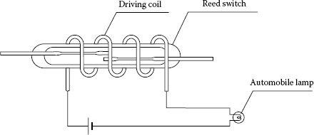
FIGURE 11.24
Lamp burnout sensor for an automobile.
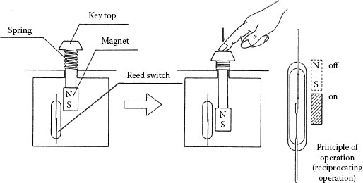
FIGURE 11.25
Key switch for use with key boards.
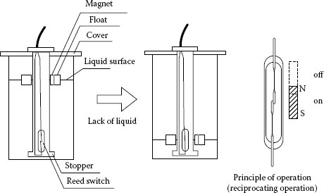
FIGURE 11.26
Float switch to detect fluid levels.
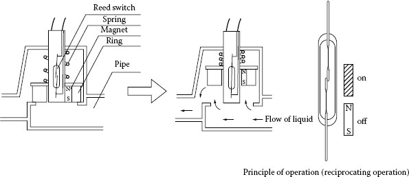
FIGURE 11.27
Flow detection switch to detect fluid motion in pipes.
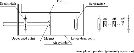
FIGURE 11.28
Air cylinder switch.
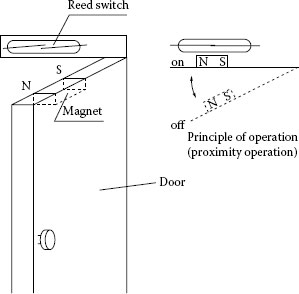
FIGURE 11.29
Door switch that detects door opening and closing.
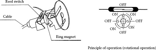
FIGURE 11.30
Speedometer switch.
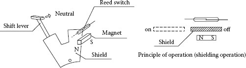
FIGURE 11.31
Neutral position detection switch.
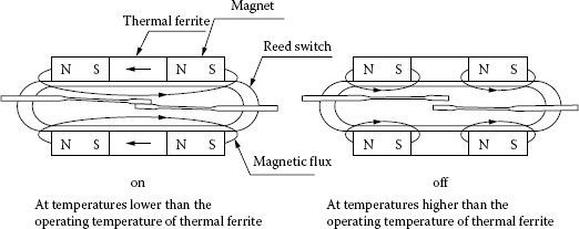
FIGURE 11.32
Principle of operating thermal switch for a wide application from electric ranges to automobile engines.
1. OM Hovgaard, GE Perreault. Development of reed switches and relays. Bell Syst Tech J 34 (2): 309, 1955.
2. LD Dumbauld. Dry reed switches. Control Engineering, July: 75, 1963.
3. HN Wagar. Some measurement techniques for characterizing sealed reed contact performance. IEEE Trans Comp Parts, December: 8, 1964.
4. R Holm. Electric Contacts, 4th ed. Berlin: Springer-Verlag, 3rd Printing, p 171, 2000.
5. T Yano, C Kawakita, M Yasuda, K Hinohara. Reed Switches. Tokyo: Oki Electric Industry, 1987.
6. C Kawakita, K Hinohara, T Kobayashi, Y Mizuguchi. Development of ultraminiature wide differential reed switches. Proceedings of the 39th Relay Conference, April 1991.
7. K Hinohara, T Kobayashi, C Kawakita. Magnetic and mechanical design of ultraminiature reed switches. IEEE Trans Comp Hybrids, Manuf Technol 15: 172–176, 1992.
8. RL Peek Jr. Magnetization and pull characteristics of mating magnetic reeds. Bell Syst Tech J 40 (2): 1961.
9. KF Bradford, FE Bader. Estimating sealed reed contact forces. Bell Lab Rec 44 (5): 1966.
10. K Kato, H Suzuki. Design of magnetic reed switch. Trans IECE J51-C (5): 211–218, 1968.
11. M Takahashi, S Yamazaki, K Kato, T Tanii, K Ono, M Nagao, M Watanabe. Development of DC-10 reed switch for DEX-2. Elect Commun Lab Tech J 18 (4): 79–99, 1969.
12. RJ Gashler. Magnetic force characteristics of electromechanical relays. Proceedings of the19th Relay Conference, pp 18.1–18.16, 1971.
13. T Yokokawa, T Yano, C Kawakita, K Hinohara, T Kobayashi. Contact surface conditions of ruthenium-plated contact reed switches. Proceedings of the 14th International Conference on Electric Contacts, pp 135–140, 1988.
14. T Yokokawa, T Yano, C Kawakita, K Hinohara, T Kobayashi. Thickness of ruthenium oxide film produced by the surface deactivation treatment of ruthenium-plated contact reed switches. Proceedings of the 35th IEEE Holm Conference on Electrical Contacts, pp 177–181, 1989.
15. L-J. Xu, JG Zhang, B Miedzinski. Modeling of vacuum reed failure by using finite element method. Proceedings of the 46th IEEE Holm Conference on Electrical Contacts, pp 115–119, 2000.
16. Y Hashimoto, K Yokoyama, T Kobayashi. A study on the contact materials for ultra-miniature reed switches. Proceedings of the 24th International Conference on Electrical Contacts, pp 113–118, 2008.
17. K Arushanov, S Karabanov, I Zeltser, R Maizels, E Moos. New technology of modification of reed switch contact surfaces with the usage of ion-plasma nitriding. Proceedings of the 26th International Conference on Electrical Contacts, pp 284–287, 2012.
18. HW Hermance, TF Egan. Organic deposits on precious metal contacts. Bell Syst Tech J 37: 739–776, 1958.
19. T Yokokawa, C Kawakita. High reliability reed switches with rhodium plated contacts. Proceedings of the 21st Relay Conference, pp 13.1–13.7, 1973.
20. K Hinohara, A Nagai. Surface deactivation treatment of rhodium-plated contact reed switches. OKI Tech Rev 52 (123): 59–63, 1986.
21. T Yokokawa, T Yano, C Kawakita, K Hinohara, A Nagai. A study on the surface deactivation treatment of rhodium-plated contact reed switches. IEEE Trans Comp Hybrids Manuf Technol CHMT 9: 124–127, 1986.
22. T Yokokawa, T Yano, C Kawakita, K Hinohara, A Nagai, T Kobayashi. A study of the thickness of rhodium oxide film produced by the surface deactivation treatment of rhodium-plated contact reed switches. IEEE Trans Comp Hybrids Manuf Technol CHMT 10: 42–46, 1987.
23. DG Castner, GA Somorjai. LEED, AES and thermal desorption studies of the oxidation of the rhodium (111) surface. Appl Surf Sci June: 28–38, 1980.
24. H Ishida, A Ishitani. Raman microprobe analysis of thin films formed on the surface of silver electrical contacts utilizing the surface-enhanced Raman scattering effect. Appl Spectrosc 37 (5): 1983.
25. AD Hamer, DG Tisley, KA Walton. X-ray photoelectron spectra of compounds containing rhodium-halogen bonds and of rhodium (II) acetate and its derivatives: rhodium 3d and halogen np binding energies. J Chem Soc Dalton 116–120, 1973.
26. JS Brinen, A Melera. Electron spectroscopy for chemical analysis (ESCA) studies on catalysts. Rhodium on charcoal. J Phys Chem 76 (18): 1972.
27. T Yokokawa, T Yano, C Kawakita, K Hinohara, A Nagai. A study on the soft sticking of rhodium contact reed switches. Proceedings of the 34th Relay Conference, pp 12.1–12.3, 1986.
28. T Yokokawa, T Yano, C Kawakita, K Hinohara, T Kobayashi. A study on the rhodium-plated contact reed switch. Proceedings of the International Conference on Electrical Contacts and Electromechanical Components, pp 254–262, 1989.
29. T Yokokawa, T Yano, C Kawakita, K Hinohara, T Kobayashi. Contact performance degradation and surface deactivation techniques. Proceedings of the 1st International Symposium on Corrosion of Electronic Materials and Devices, Vol. 91-2, pp 423–429, 1991.
30. K Hinohara. Tribology in electrical contacts. J Jpn Soc Tribol 39 (5): 447–450, 1994.
31. N Wakatsuki, A Yamamoto. Bouncing of a reed switch due to coulomb’s electrostatic force. Proceedings of the 52nd IEEE Holm Conference on Electrical Contacts, pp 165–169, 2006.
32. K Hamada, Y Shimizu, S Umezaki. Applications of heavy-duty reed switches. Proceedings of the 23rd International Conference on Electrical Contacts, pp 534–540, 2006.
33. S Day, T Christenson. A high aspect ratio micro-fabricated reed switch capable of hot switching. Proceedings 59th IEEE Holm Conference on Electrical Contacts, pp. 336-343, 2013.