
Plug-in connectors are in common use for connecting equipment to a busway. Devices connected to busways cover a wide range of industrial control equipment ranging from individual circuit breakers to feeders for panel boards. Under certain conditions, fretting can occur in the connector-busbar interface owing to the same type of relative motions as in the bus-stub contacts as discussed above. The connector assemblies used in these applications must reliably conduct currents ranging from 100 A to several thousand amperes throughout the lifespan of the bus duct system. Thiesen and Forsell [69] designed a special fretting testing system to investigate the performance of a typical 200 A plug-in connector under fretting conditions. Tests were carried out on the silver-, tin-, and cadmium-plated contact surfaces showed that fretting produced significant contact damage as manifested by the large accumulation of the fretting debris in the contact zones which resulted in high contact resistance. The authors concluded that this fretting testing system can be an excellent tool in comparative analysis of the design requirements for connector systems.
It is generally accepted that the reliability of bolted joints is attributed to high contact forces and large apparent contact areas with virtually no relative displacement between the contacting members. Although this may hold for copper-copper joints, it is certainly not necessarily the case for aluminum-copper connections. This is because the coefficient of thermal expansion of aluminum is 1.36 times that of copper and when a bolted aluminum-copper joint is over heated by the passage of current, aluminum will tend to expand relative to copper causing displacement of the contact interface. The shearing forces generated by differential thermal expansion will rupture the metallic bonds at the contact interface and cause significant degradation of the joint. Published experimental evidence and reports of trouble in service show that bolted joints may not be as impervious to degradation and failure. The effect of relative motion in aluminum-copper bolted joints has been investigated in the laboratory by Bond [70], Naybour [71], Jackson [14], and Roullier [72] who have shown that the relative displacement induced by differential thermal expansion forces is one of the major degradation mechanisms of aluminum-copper joints. Yet, despite the seriousness of this problem, there is very little published information linking field failures with the degradation effects of relative motion (fretting) in bolted joints.
Recently, fretting damage in real life tin-plated aluminum and copper connectors, commonly used for distribution transformers, has been reported by Braunovic [73,74]. The connectors examined had been removed from the service after 7–10 years of service owing to either overheating, as discovered by routine thermography inspection, or unstable performance on the network under normal operating conditions. The connectors were bolt-type tin-plated aluminum or copper busbars jointed with either tin-plated or bare aluminum cable terminals. A typical example of the connectors with signs of severe fretting damage as manifested by a characteristic set of accumulated fretting debris and oxides is shown in Figure 5.34. The significant feature of these events is that fretting causes serious damage to the contact areas. Examination of these areas reveals the presence of four distinct forms of fretting damage: electrical erosion by melting/arcing (region 1, Figure 5.34a), accumulation fretting debris, delamination and abrasion. The results of contact resistance measurements across the contact zone of a tin-plated copper connector are shown in Figure 5.35. The most important feature is that the contact resistance of the zones severely damaged by fretting increases rapidly to very high values, and in some locations, open-circuit conditions developed. These results correlate well with those obtained under controlled laboratory conditions showing that fretting causes the contact resistance of tin-plated contact to increase at very rapid rates. The cyclic nature of the contact resistance, manifested by sharp fluctuations from one site to another, indicates that the fretting debris formed on the connector surface is not a continuous layer but rather porous, since the transition from high-to low-conducting current paths occurs over relatively short distances. Another interesting feature of these events is the presence of a region around the bolt with very low contact resistance values. This can be associated with the formation of good metallic contact with the load-bearing area under the flat washer where the contact pressure is highest. Detailed SEM examination of these zones shows no evidence of severe fretting damage or accumulation of fretting debris. Instead, the grainy texture of the tin-plating was heavily deformed and compacted, as revealed by the presence of areas with smooth surfaces with clearly visible scars of mild abrasion. The results of x-ray diffraction analysis of the fretting debris removed from the damaged contact zones of tin-plated aluminum connectors showed that the fretting debris was composed mainly of tin but the presence of Al (OH)3 was also detected, indicating that the corrosion products of aluminum were also prominent constituents. This suggests that fretting was not the sole mechanism responsible for the observed degradation of tin-plated connectors and that corrosion also played a very important role. The presence of corrosion products in the contact zones indicates that the introduction of an aqueous solution to a fitting environment may influence the fretting process in one or both of two distinct ways. Firstly, the liquid can serve as a lubricant, so separating the metal surfaces and reducing adhesion, friction and wear rate. Secondly, a liquid may induce an anodic corrosion reaction within the fretting scar, trapping the corrosion products inside the fretting scars and therefore increasing the rate of wear.
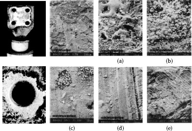
FIGURE 5.34
Typical example of a tin-plated connector removed from service with signs of severe fretting damage as evidenced by a characteristic band of accumulated fretting debris and oxides and SEM surface analysis of typical fretting damage in aluminum-to-tin-plated copper connection: (a) Electrical erosion (region 1); (b) Accumulation of fretting debris and oxides (region 2); (c) Delamination wear (region 3); (d) Abrasion (region 4); and (e) Combined delamination-abrasion wear.
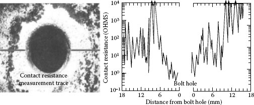
FIGURE 5.35
Variation of contact resistance with the distance from the bolt hole in the contact zone of a tin-plated copper connector.
Tin and tin alloys are used extensively in a variety of applications in the electronic and electrical industries either as solders or as coatings to aid soldering or to mitigate galvanic corrosion when dissimilar metals like copper and aluminum are in contact, Such widespread use prompted numerous investigations into determining the parameters for ensuring satisfactory and reliable operation of these joints. As a consequence, it is now well-established that the formation of intermetallics, corrosion and fretting are the most serious degradation mechanisms impairing the reliable operation of tin and tin alloy connections. Although the nature of these degradation mechanisms is different, they all have an adverse effect the contact resistance of a connection.
Systematic studies of dry tin-plated connection failures have established that fretting is probably the foremost detrimental mechanism to the performance of a connection involving tin and tin alloys. Dry tin-plated contacts are the most susceptible to fretting damage, since hard tin-oxide particles easily abrade the contacting, metals thus alleviating the oxidation of exposed materials and accumulation of highly insulating fretting debris at the contact interface. As a result, the contact resistance will increase at very high rates thus raising the joint temperature which, will accelerate the deterioration of the contact members. A typical example of the deleterious effects of fretting in tin-plated contacts is shown in Figure 5.36. It is seen that contact resistance increases rapidly after only a few hundred cycles, eventually leading to an open circuit condition. This takes place over a wide range of contact loads and becomes worse with increasing slip amplitude. The consequences of such a dramatic increase in the contact resistance are, initially, Joule heating of the contact spots followed by melting, sublimation and decomposition of the oxides and vaporization of the tin. This is illustrated in Figure 5.37 showing the contact voltage as a function of the fretting cycles. Two sustained plateaus in the contact resistance characteristics are present: one coinciding with the melting voltage of tin, corresponding to the melting temperature of tin, that is, 232°C, the other in the range where tin oxides melt and tin vaporizes. Note that the voltage range for the second plateau corresponds to the temperature range of 1000–3000°C.
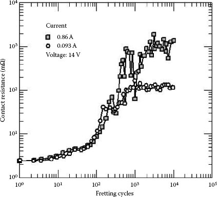
FIGURE 5.36
Typical examples of deleterious effect of fretting in tin- and solder-plated contacts.
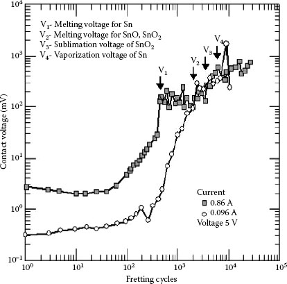
FIGURE 5.37
Contact voltage as a function of fretting cycles.
It should be pointed out, however, that despite the widespread use of tin and tin-alloys as contact materials (plating) in a variety of high power connector systems, very little published information about failures owing to fretting is available. It is virtually certain that fretting has a significant influence on the performance of tin-plated power electrical connections and therefore deserves more attention than accorded in the past. Jackson [67] who found that a dramatic resistance changes are produced during heating and cooling of a tin-plated aluminum–copper joint. The progressive deterioration was attributed to the relative motion generated at the contact interface by the differential expansion forces between the substrates of aluminum and copper induced during heating and cooling of the contact assembly.
5.4.11.7.2 Silver and Silver Alloys
Owing to its nobility, silver and silver alloys have been widely used in high power electrical applications where high conductivity of the contacting interface is essential. It is generally believed that fretting is not a serious problem in silver-bearing contact, although recently Kassman et al. [61] have reported that fretting can produce severe deterioration of the power contacts. The tests were conducted on contacts made of copper rods electroplated with 5 and 17 μm of silver using cross-rod geometry. The frequency was 100 Hz and the vibration amplitude was varied from 20 to 70 μm. The contact force was varied from 5 to 50 N. The current was 10 or 100 A DC and the test durations were 2 and 20 minutes. The type of contact mechanism produced under dry weather by the vibration motion was found to vary drastically depending on the contact force and vibration amplitude. In the case of unlubricated contacts after 2 minutes of vibration four contact deformation mechanisms were distinguished, in the case of unlubricated contacts. Their occurrence could be mapped in the amplitude/contact force plane, seen in Figure 5.38. Coating thickness variations do not seem to specify which characters are included in the map, but serve rather to move their borders and the margin between the seizure and non-seizure zones. Furthermore, the damage can also vary with time, that is, the amount of material transfer and extrusion increases and the effect of fretting corrosion on exposed copper becomes obvious. The changes in the contact resistance for the four types of fretting damage observed are illustrated in Figure 5.39. For all damage types the contact resistance dropped from a slightly higher initial value to around 15 μΩ after a few seconds. After some 2 minutes the resistance starts to escalate for Types C and D. This is because both types quickly expose copper in the contact area, which is twisted into an insulating copper oxide layer by fretting corrosion. After 20 minutes, the contact resistance had increased approximately 1000% for Type C, which was the worst type. Type B showed a moderate 70% increase while Type A showed no increase even after trying for a long time and remained still consistently low after 2000 minutes.
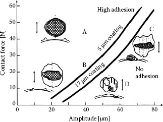
FIGURE 5.38
Mapping of the damage mechanisms as a function of contact force and vibration amplitude 52.
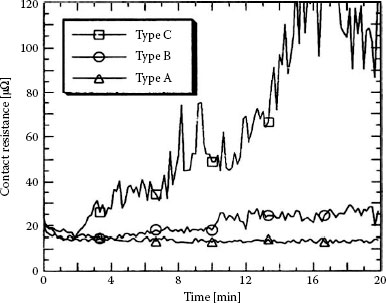
FIGURE 5.39
Contact resistance variation with fretting time in silver-plated copper.
5.4.11.8 Fretting in Aluminum Connections
The deleterious effects of fretting are of particular interest in aluminum connections since aluminum exposed to the atmosphere rapidly oxidizes, forming an oxide film within a very short time. Hence, under fretting conditions, accumulated wear debris and oxides cannot be effectively removed from the contact zone and a highly localized, thick insulating layer is formed leading to a rapid increase in contact resistance and, subsequently, to virtually open circuits. The performance of aluminum conductors in contact with different plating and base metals under fretting conditions has been extensively studied by Braunovic [54,55,56,57,58,73,74,77,78,79] who has shown that fretting adversely affects the contact behavior of aluminum in contact with practically all common contact materials. Some typical examples of such behavior are shown in Figure 5.40. The effect appears to be characterized by three points:
1. The contact resistance remains virtually unaffected by the fretting action and can be explained as follows. When the contact is made, surface asperities will penetrate the natural oxide films, thereby establishing localized metallic contacts and, conducting paths. The number of conducting paths thus established will not be greatly affected by the fretting-induced displacement of the contact interface, since the wear products formed will be predominantly composed of metallic particles, thus a relatively good electrical contact will be maintained.
2. Further fretting will force the wear debris to escape and allow the establishment of a larger number of metallic contacts. Consequently, a good metallic contact between contacting surfaces will be established and maintained, resulting in a very low, practically fluctuation-free contact resistance. The cyclic nature of the contact resistance, manifested by short-term fluctuations, is most likely owing to temporary rupture of the oxide layers and the appearance of local metallic contacts, which provide good conducting paths. The persistence of these fluctuations indicates that the generation of conducting spots by mechanical rupture of the intermediate layers of oxides and fretting debris is counterbalanced by the closure of the paths newly formed by the fretting action.
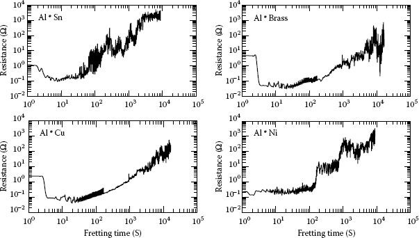
FIGURE 5.40
Typical contact resistance behaviour of aluminum in contact with common contact materials under fretting conditions: slip amplitude 25 μm; contact load 2 N; frequency 0.005 Hz
3. After prolonged exposure to the fatigue-oxidation process, metallic layers in the contact zones soften and progressively separate. The contact zone now consists of a thick insulating layer containing oxides and wear debris, and any remaining metallic contact is lost, causing a sharp increase in the contact resistance. The cyclic nature of the latter is owing to the temporary rupture of the insulating layer by fritting and the appearance of localized metallic conducting paths formed as a result of contact self-healing [12]. Subsequent wiping will fracture these conducting bridges and the contact resistance will rise, which in turn will further increase the contact spot temperature up to melting, sublimation and decomposition of the oxides and even vaporization of the contact materials.
Fretting of aluminum causes an extensive exchange of materials in the contact zones. Some representative examples of the Scanning Electron Microscope (SEM) and Energy Dispersive X-Ray Analysis (x-ray mapping, EDX) of material transfer in the aluminum-to-tin plated brass connections are shown in Figure 5.41. The deleterious effects of fretting can be greatly reduced by applying higher contact loads and/or lubricants to the contact zones. When higher load is applied, the onset of the thermal runaway condition can be delayed since much higher contact resistance is needed to reach the contact voltage or spot temperature required for this to happen. The effect of contact load is of considerable practical importance because of aluminum has an intrinsic tendency to creep and stress relaxation, which can result in the loss of a contact and consequently accelerate the degradation of a connection with the ever-present fretting action. It is therefore essential to maintain high contact pressures in all electrical connections in order to assure sufficiently large current-carrying areas and the mechanical integrity of a joint.
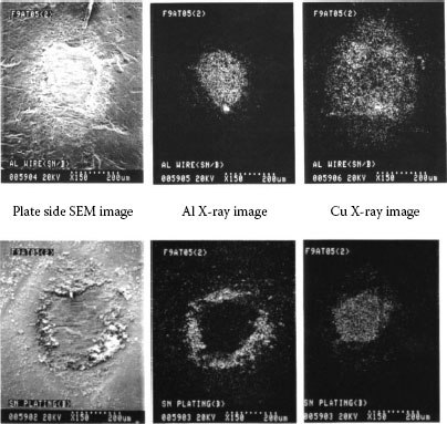
FIGURE 5.41
SEM micrographs of fretting damage in contact zones of an aluminum conductor in contact with tin-plated connections. The X-ray images of Al, Cu, and Sn exemplify the transfer of materials in both directions. Light areas depict the fretting debris.
5.4.11.9 Effect of Electrical Current
The result of fretting in copper-to-copper contacts under AC (60 Hz) and DC current conditions was investigated by Gagnon and Braunovic [78]. It was demonstrated that the overall contact resistance behavior of copper-to-copper wire-plate couples under AC and DC current was practically the same as pictured in Figure 5.42. Fretting debris in the samples fretted under DC current are compacted without flake-like plates, Figure 5.43. Furthermore, the fretting damage in samples operating under AC current is more pronounced and characterized by the presence of flake-like debris that was not observed in the samples operating under DC current as clearly depicted in Figure 5.43. The characteristic feature of the samples under AC current conditions is a pronounced distortion of the contact voltage (see Figure 5.44) and the presence of large amounts of flake-like fretting debris widely scattered around the contact zone.
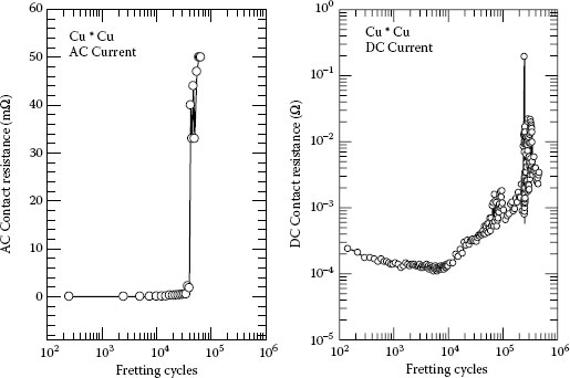
FIGURE 5.42
Effect of fretting on the AC and DC contact resistance of copper-to-copper wire-plate contacts. Fretting conditions: contact load 400 g, fretting frequency 1 Hz, slip amplitude 100 μm current 50 mA.
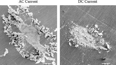
FIGURE 5.43
SEM images of the contact zones after 40,000 fretting cycles under AC and DC current conditions. (From M. Braunovic, Electric Contacts-1989, San Francisco, 1989, p. 179.)
5.4.11.10 Fretting in Coatings (Platings)
Presently, electronic and electrical industries are experiencing a relentless increase in the use of protective and wear-resistant coatings for electrical contact applications. Such movement is driven not only by the cost benefit demands but also useful functions offered by the coatings such as: corrosion and wear protection, diffusion barriers, conductive circuit elements, fabrication of passive devices on dielectric surfaces and others (See Chapter 8). The performance of an electronic/electrical connector is essentially controlled by the surface phenomena such as pollution, oxidation, re-oxidation, sulfide-formation, corrosion, etc. The presence of these contaminants on the surface increases the contact resistance and is detrimental to the connection reliability. Examples of the effect of coating materials on the contact resistance and coefficient of friction on the fretting behavior of different plating materials are indicated in Figure 5.45 [79]. It should be noted that despite the obvious advantages of the coatings, there are still a number of factors such as surface imperfections (porosity), hardness (soft), adherence to the substrate and resistance to oxidation and the effects of a corrosive environment are probably the most important affecting the characteristics of practically all types of coated electrical connections.
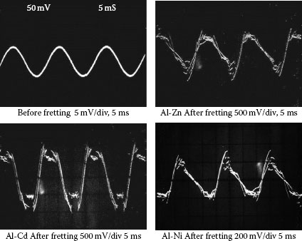
FIGURE 5.44
Effect of fretting on the AC waveform signals.
5.4.11.11 Fretting in Circuit Breaker Terminal Contact Materials
Although there is only limited data described in the open literature on fretting problems with circuit-breaker contact materials, the above discussion on the deleterious effects of fretting in power contacts may be equally applied to circuit-breakers. Ambier and Perdigon [81] have designed a special test system to simulate the real-life operation of a circuit breaker and used it to investigate the degradation of the contact materials by fretting. The contact materials examined were copper (OFHC and copper-tellurium alloy) and tin-, nickel-, and silver-coated copper and aluminum alloy (6061 grade). Tests were conducted at contact loads of 10–30 N, oscillation frequency 20–300 Hz, slip amplitude 25–200 μm and with current in the range 10–250 A. It was shown that as a result of fretting severe damage occurred in the contact zones of almost all the materials tested. The most stable performance was observed in the aluminum contacts coated with 150 μm thick silver layer. However, the stability of silver-coated contacts was greatly influenced by the contact load, coating thickness and processing methods and slip amplitude. Commercially available silver-coated aluminum with 7 μm layer of silver and with 15 μm nickel underlayer showed an erratic behavior under different fretting conditions. At low contact loads, a very unstable contact resistance behavior was observed whereas at higher loads higher wear rates dominated.
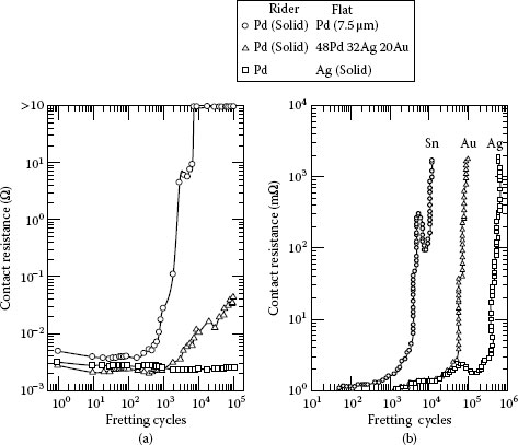
FIGURE 5.45
Contact resistance of (a) solid palladium fretting against palladium- and PdAgAu-plating and solid silver and (b) tin-plated spherical pin (rider) fretting against tin-, gold-, and silver-plated flats.
5.4.12 Intermetallic Compounds
Bimetallic welds, particularly, aluminum-to-copper are increasingly being utilized in a variety of electrical applications. Such joints, caused by friction welding, pressure welding, diffusion and roll bonding, flash welding and explosion welding, are characterized by a relatively stable joint interface and negligible intermetallic formation. In service, however, frequent current surges on the network may generate favorable conditions for inter-diffusion to occur and, thus, nucleation and growth of intermetallics at or near the initial interface. This, in turn, can seriously impair the overall electrical stability and mechanical integrity of bimetallic joints since intermetallic phases have much higher electrical resistance and lower mechanical strength (See Chapter 1, Section 1.3.3). Some authors found that tensile strength, ductility, impact resistance and electrical resistance of flash-welded aluminum-to-copper joints are practically unaffected by thermal treatment for two years at 149°C to 5 minutes at 371°C [82]. Investigations of roll-bonded [82,84], hot-pressed [75] and flash-welded [75,76] aluminum-to-copper joints show that the mechanical and electrical properties are significantly affected by the formation and growth of intermetallics at the joint interface. It was shown that, when the total width of intermetallic phases exceeds 2–5 μm the aluminum-to-copper joint rapidly loses its mechanical integrity [85,86].
Figure 5.46a depicts the intermetallic phases formed at the interface of an aluminum-copper contact while in Figure 5.46b is shown the nanohardness traverse of the intermetallic phases formed at the aluminum-copper interface in samples diffusion annealed. The composition and characteristics of intermetallic phases formed in the aluminum-to-copper joints are shown in Table 5.6. To illustrate the importance of interdiffusion and the formation of intermetallic compounds, let us use the following example. The process of diffusion is controlled by the following expression:
(5.15) |
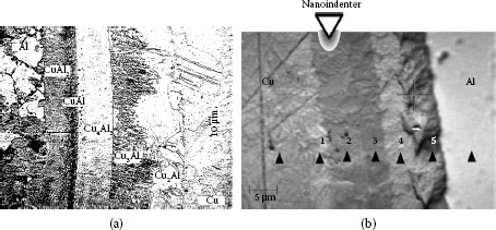
FIGURE 5.46
(a) Microstructure of the intermetallic phases formed at the interface of Al–Cu contact under the influence of thermal gradient; (b) Nanohardness traverse of the intermetallic phase formed at the copper-aluminum joint interface.
TABLE 5.6
Important Characteristics of Intermetallic Phases Formed in Bimetallic Al-Cu
where Do is a constant, Q is the activation energy for diffusion and R is the universal gas constant. In the case of aluminum-copper, the activation energy for diffusion of aluminum is Q = 40 kcal/mole. Hence the diffusion rates at temperatures T1 and will be
(5.16) |
Using Equation 5.16 the temperature rise required to double the diffusion rate at T1 = 60°C is calculated to be ΔT = 4°C. Bearing in mind the fact that, owing to the current constriction, the a-spot may develop a higher temperature, the diffusion rates at the a-spot can be considerably higher than in the bulk. To prove this point, let us assume that the a-spot is at T2 = 300°C and the bulk at T1 = 60°C. Then the calculated diffusion rate at the a-spot will be 1012 faster than that in the bulk. Under these conditions, the formation of intermetallics is very likely to happen.
Accelerated diffusion can occur via some short-circuit diffusing paths rather than through the lattice. Such paths, called “pipe diffusion,” can be dislocations, grain and subgrain boundaries. Diffusion along these paths is found to be considerably faster (a few orders of magnitude) than diffusion of the same species through the lattice [87]. Another mechanism that can enhance mass transfer across the contact sport is electromigration. Runde [88] has shown that high-current density can provoke mass transport by electromigration through the contact spots. As a result, accumulation of vacancies at some distance inside the contact will occur, leading to the formation of vacancy clusters and voids which, in turn, will reduce the mechanical strength of the contact area.
Gusak and Gurov [89] and Pimenov et al. [90] who have shown that the current has a considerable effect not only on diffusion but also on the kinetics of nucleation and formation of phases in bimetallic systems. Braunovic and Alexandrov [91] investigated the effect of electric current on the morphology and the dynamics of formation of intermetallic compounds of bimetallic friction-welded aluminum-copper joints, see Table 5.6. The establishment and growth of intermetallic compounds were analyzed in the temperature range 200°C–500°C realized by heating Al–Cu joints with an AC current of different intensities (400–1000 A). It was demonstrated that electrical current accelerates the kinetics of formation of intermetallic phases and significantly alters their morphology in bimetallic aluminum-to-copper friction-welded joints.
The growth kinetics of intermetallic phases under the influence of electrical current is much higher than under diffusion annealing in a temperature gradient. The growth rate of the intermetallic phases was determined by measuring the thicknesses of the interdiffusion layers (x) after selected time intervals (t) at each of the diffusion-annealing temperatures using the following expression (see Section 1.3.3):
(5.17) |
where D is the interdiffusion rate constant at the selected temperature. The thicknesses of intermetallic phases formed by diffusion annealing by an electrical current and in a temperature gradient are given in Tables 5.7 and 5.8. The activation energy characterizing the rate of formation of the intermetallic phases is given as
(5.18) |
where Do is a constant, Q the activation energy, T the temperature and R the universal gas constant. The reaction rate constant (D) calculated from the slope of (D)1/2 of each curve is plotted versus 1/T in Figure 5.47. In both cases, the rate of formation of intermetallic phases in samples diffusion-annealed in an electrical field gradient could not be identified by the single activation energy over the entire temperature range studied but rather by considering the two separate areas, that is, 200°C–300°C and 350°C–500°C.
TABLE 5.7
Thickness (μm) of Intermetallic Phases Formed in Aluminium–Copper Bimetallic Joints After Diffusion Annealing by an Electric Current
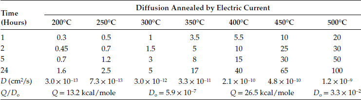
TABLE 5.8
Thickness (μm) of Intermetallic Phases Formed in Aluminum–Copper Bimetallic Joints After Diffusion Annealing in a Furnace
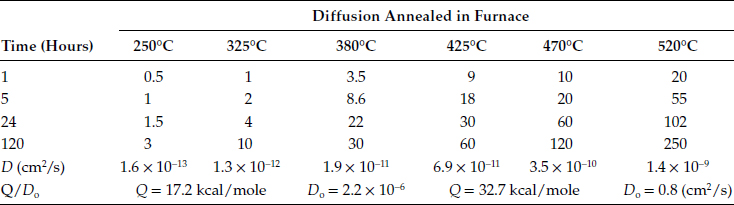
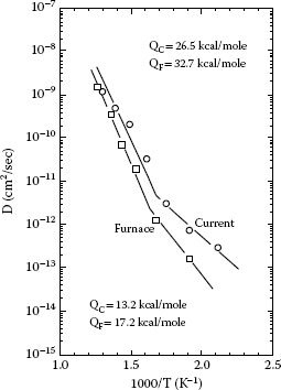
FIGURE 5.47
Arrhenius plot of the rate constant for growth of the diffusion layers in aluminum–copper bimetallic contacts diffusion annealed in temperature and electrical field gradients.
The activation energy corresponding to temperatures below approximately 350°C is considerably lower (QC = 13.3 kcal/mol) than that obtained for higher temperatures (QC = 20.5 kcal/mol). It is also important to note that for the same temperature range, these values are significantly lower than those obtained for the samples diffusion annealed in a furnace, that is, Q = 17.2 kcal/mol and Q = 32.2 kcal/mol. The same type of behavior was reported by Timsit [92] in aluminum-brass contacts diffusion annealed in a temperature gradient. The activation energies in the temperature range 150°C–300°C and 350°C–450°C were almost identical to those measured in the Al–Cu bulk diffusion couples. It was demonstrated that both the pace and the total diffusion bandwidth of the intermetallic phases formed under the influence of electric current are higher than in samples diffusion-annealed in furnaces. It is interesting to note, that these results are in contrast with those obtained in the case of roll-bonded aluminum-brass couples since no effect of electrical current on the intermetallic growth was found in this system [93].
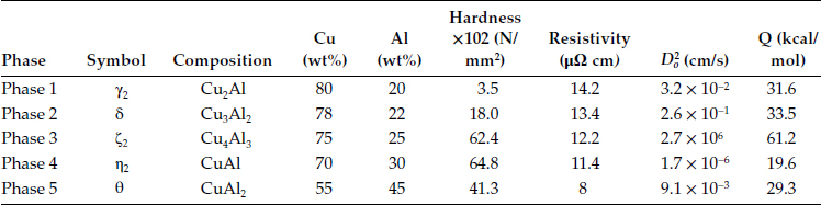
The most characteristic feature of the microstructure of the Al–Cu interface after diffusion annealing by an electric current is that, over the entire temperature range investigated, the interdiffusion layer consisted basically of four major bands (Cu2Al, Cu4Al3 CuAl and CuAl2), as seen in Figure 5.48. The compositions formed are given in Table 5.6. The impaired mechanical integrity of the Al–Cu bimetallic joints treated by an electric current is clearly evidenced by extensive cracking not only across the whole intermetallic bandwidth but also within different phases and at a neighboring interface as seen in Figure 5.49. It is clear that complex structural processes occur at the contact interface during the action of the electric current, following which the mode, the kinetics of formation, and the development of the intermetallics are significantly altered. The question immediately arises as to whether the formation of intermetallic phases within the allowable operating temperature range in an electrical connection, generally reckoned to be 100°C–150°C, is sufficiently fast to produce an appreciable effect on the functioning of a connector that otherwise follows the requirements generally determined by the existing standards.
Using the experimentally found values of the activation energies (Figure 5.47), the thicknesses of the intermetallic layers formed in aluminum-copper were calculated for different time intervals at 100°C, 150°C, and 200°C and are depicted in Figure 5.50. Since electrical connections operating under network overload conditions often experience temperatures of 200°C and above, these temperatures were included in the calculation. It is clear that at 100°C, the growth kinetics is relatively slow. However, at 150°C and 200°C, the rate of intermetallic growth is quite appreciable. It is interesting to note that the rate of intermetallic growth in samples treated by an electric current is roughly twice as high as that of samples diffusion-annealed in a furnace.
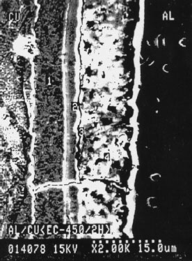
FIGURE 5.48
SEM micrograph of the intermetallic phases formed in the bimetallic Al–Cu contacts after 2 hours of diffusion annealing at 450°C by an electrical current.
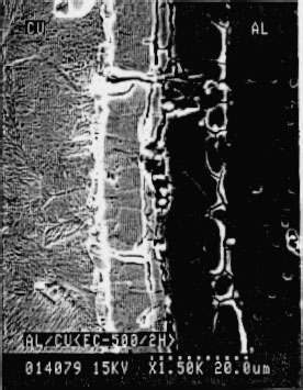
FIGURE 5.49
Cracks formed in bimetallic layers illustrating the fragility of intermetallic phases formed at bimetallic Al–Cu contact. Microhardness of copper and aluminum are respectively 42 and 38 kg/mm2.
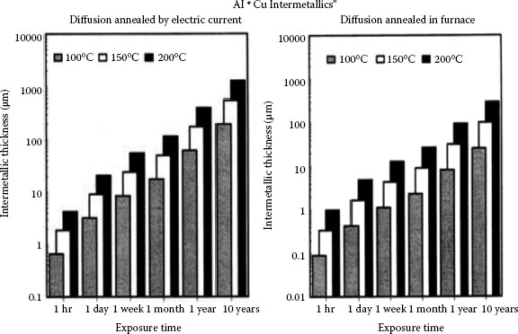
FIGURE 5.50
Calculated thicknesses of the intermetallic phases formed in Ai–Cu bimetallic contacts following diffusion-annealing in thermal and electrical field gradients for different times at 100°C, 150°C, and 200°C.
The mechanical properties of aluminium–copper are strongly affected by the presence of the intermetallics when their thickness at the interface reaches the critical value of 2 μ m. At this thickness, the interface between the two metals in contact becomes brittle, therefore creating the interface highly porous, more susceptible to adverse environmental effects and generation of numerous fissures in the interdiffusion layer [94]. From Figure 5.50 it appears that the critical thickness of 2 μm can be reached after a few days of exposure to 100°C produced by the electric current. If such is the case, this finding can have serious implications for the mechanical integrity of Al–Cu electrical connections. The effect of electric current on the formation and growth of intermetallic phases therefore deserves more attention because the electrical connections are constantly subjected to the action of electric current.
The formation of intermetallic phases has an extremely detrimental effect on the electrical resistance, as demonstrated by dramatic increases in the contact resistance. A direct consequence of higher resistance is heating of the contact, which results in an increased rate of formation of intermetallic phases and as well as other degradation processes such as creep, stress relaxation, fretting, oxidation, etc. The effect of intermetallic phases formed at the Al–Cu interface on the contact resistance is shown in Figure 5.51.
(5.19) |
Within the scatter of experimental data, the rate of resistance rise across the Al–Cu interface and thickness (x) of the intermetallic layers formed can be approximated by a linear relationship
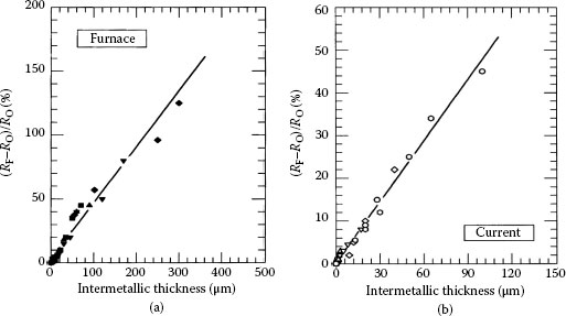
FIGURE 5.51
Growth of contact resistance with thickness of the Intermetallic phases formed in Al–Cu bimetallic contacts after diffusion annealing by a temperature and electrical field gradients.
(5.20) |
Where Ro and RF are respectively the resistances measured across the Al–Cu interface before and after diffusion treatment of an electric current; C is the proportionality constant having the value 0.4 for the samples diffusion annealed in a temperature gradient and 0.48 for the samples annealed by an electric current. The resistivity of the intermetallic layers in the aluminum-to-copper bimetallic joints can be expressed as
(5.21) |
where xt is the thickness of the total intermetallic layer (microns); ρAl = 2.4 μΩ cm and ρCu = 2.0 μΩ cm—are the resistivity of aluminum and copper respectively; ; D = 0.3 cm is the spacing between the potential probes. The calculated value of the resistivity of the total intermetallic layer in Al–Cu heat-treated solid-phase joints is ρt = 18.5 μΩ cm. The resistivity values for the individual phases range between 8 and 14.2 μΩ cm (Table 5.6). The observed difference exceeds the experimental error indicating that there are additional contributions to the total resistivity.
It is believed that these contributions can be attributed to porosity, cracking, grain size changes and increased dislocation density in the diffusion zone. These defects constrict the current flow across the interface and thus considerably reduce the effective contact area. As a result, the resistivity of the total intermetallic layer increases. One plausible explanation is that the observed effect might be associated with the material transport by electromigration [94]. The transport phenomenon, first reported in 1861, and was termed as electromigration. Conceptually, electromigration may be considered as current-induced diffusion. In any region in the material where conditions exist that make an atomic jump in one direction more probable than another, a net mass flow may occur. This process of current-induced mass flow takes place only in the immediate vicinity of the contact spots. In electromigration material transport occurs via interaction between the atoms of a conductor and a high density current of the order of 103–105 A/cm2. The drift velocity varies strongly with temperature and is particularly high along grain boundaries, dislocations and other lattice defects. The migration velocity v of the atom is given by
(5.22) |
where j is the current density, Δ the electrical resistivity, Z* the dimensionless term regarded as the effective valence or charge number of the ion, D the diffusion coefficient, k the Boltzmann constant and T the absolute temperature.
Modern studies [94,95] of aluminum electromigration have centered on the reliability of thin-film interconnections in microcircuit applications. Reduction of the conductor line width to enable the circuit density to be increased has brought the current density in aluminum thin-film “wiring” up to a range where electromigration failure (open circuit) has become a reliability concern. Investigations in this regard have generally focussed on DC applications. Although electromigration has not previously been associated with the deterioration of contact spots, the current density in the a-spots of a practical contact can be substantially higher than in the thin-film interconnections of an integrated circuit. It is therefore suggested that electromigration is of considerable importance for the reliability and degradation of bulk electric contacts.
Electromigration deterioration of a-spots in aluminum contacts has been studied by Runde [96] in Al–Al and Al–AlZn alloys using both AC and DC currents. It was shown that mass transport by electromigration appears to influence both the mechanical and the electrical properties of a contact spot. In aluminum contacts, the atoms tend to migrate toward the anode, and hence an accumulation of vacancies occurs a short distance inside the cathode contact member. The high vacancy concentration causes considerably lower mechanical strength and higher electrical resistivity in these areas. Degradation with DC was demonstrated, but AC results were inconclusive owing to the unstable electrical behavior of the specimens.
Aronstein [97,98] has investigated AC electromigration and compared the results with DC under otherwise identical conditions. The specimens tested were two-dimensional models of asperity contact junctions, made of solid metal configured to avoid experimental scatter owing to many of the variables inevitably encountered in experiments utilizing actual contact interfaces. In order to obtain the most reproducible and meaningful results, the actual metallic current-carrying area of the “a-spot” constriction was carefully controlled. The experimental results demonstrated electromigration failure with AC as well as DC. No significance was attached to the observed difference in median time-to-failure, since the sample size for each condition tested was relatively small. Electromigration in AC applications is expected in aluminum connections when current density through the a-spots is high. With AC, the aluminum atoms in a-spots at the contact interface may be considered to have double the number of available paths (relative to DC) by which to move out of the high-current-density neighborhood, but only half the current-application time in each direction. Conceptually, all other factors being equal, AC electromigration deterioration of a-spot should therefore be about the same as DC.
Electromigration is not expected under low-current density conditions. Therefore, a comparatively low density AC current (<103 A/cm2) alone are unlikely to cause electromigration, thus, to be the operating mechanism responsible for the observed accelerated formation of the intermetallic phases in electrically heat-treated Al–Cu bimetallic joints. An alternative is that the accelerated formation of the intermetallic phases is a result of an enhanced diffusion of some species, most probably copper. The enhancement may result from the concentration of vacancies and interstitials exceeding their respective equilibrium values, thus increasing proportionally the contributions from the vacancies and interstitials to the diffusion rates.
Another possible mechanism is that accelerated diffusion occurs via some short-circuit diffusing paths rather than through the lattice. Such short diffusion paths, called “pipe diffusion” can be dislocations, grain and subgrain boundaries [87]. If “pipe diffusion” is the operating mechanism, then the kinetics of intermetallic phase formation and growth leads to the conclusion that the mobility of the diffusing species, probably copper, is much greater in the presence of an electric field than in the temperature gradient. Hence, it is believed that interaction between the applied electric field and lattice defects notably dislocations and grain boundaries, enhance the migration of the diffusing species along these short-circuit diffusion paths and thus accelerate the formation of intermetallics. The absence of certain phases in samples heat-treated by an electrical current can be attributed to the increased incubation time of some phases owing to the presence of an electrical field. In other words, the growth of these phases from their critical nuclei is suppressed by diffusion interaction with the critical nuclei of neighbouring phases having greater diffusion permeability [87].
5.4.13 Intermetallics in Copper–Tin Systems
In view of the fact that the power connections are operating at relatively high temperature, possibly 100°C, the formation of intermetallics at the copper-tin plating interface becomes an important issue. The formation and development of these phases will affect both electrical and mechanical properties of the contact interface. Figure 5.52a illustrates some typical morphological characteristics of the intermetallic phases formed during diffusion annealing by thermal gradient. The EDX elemental composition analysis of the intermetallic phases formed indicated that the phase 1 corresponds to Cu3Sn while phase 2 to Cu6Sn5. Figure 5.52a shows the SEM image of these phases formed at the interfaces of tin-coated copper while Figure 5.52b shows the elemental X-ray line scan of Sn cross the tin-coating. Flexible connectors often referred to as expansion joints, jumpers, braids, braided shunts are widely used in power generating stations and substations. Their primary purpose is to establish continuous current transfer, for example, between rigid busbars, tubular conductors or current-carrying parts of other electrical equipment such a power meter, disconnect switches etc. Flexible connectors are created by compressing the copper or tinned copper ferules with inserted ends of stacks of copper or tinned copper laminates or bundles of braided wires. In order to maintain mechanical and electrical uniformity the sides of ferrule are often soldered. The characteristic feature of the intermetallic phases formed in tin-plated copper is that these phases are significantly harder than the base material (copper) thus making these susceptible to brittle facture. The composition, physical and mechanical characteristics of intermetallic phases formed in the tin-copper systems are shown in Table 5.9.
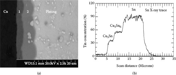
FIGURE 5.52
(a) SEM micrograph of the intermetallic phases formed at the copper-tin interface in tin-plated copper wires. Note the presence of two distinct phases (1) Cu3Sn and (2) Cu6Sn5 (b) Tin x-ray scan across the copper-tin interface of tin-plated copper wires showing the phases Cu3Sn and Cu6Sn5.
TABLE 5.9
Room Temperature Properties of Intermetallic Compounds, Copper and Tin
Cu6Sn5 |
Cu3Sn |
Cu |
Sn |
|
Hardness VHN (MPa) |
378.0 |
343.0 |
369 |
51 |
Elastic modulus (GPa) |
85.56 |
108.3 |
115 |
47.0 |
Thermal expansion (PPM/°K) |
16.3 |
19.0 |
16.5 |
23.0 |
Heat capacity (J/g/°K) |
0.286 |
0.326 |
0.385 |
0.226 |
Resistivity (μΩ cm) |
17.5 |
8.93 |
1.65 |
11.6 |
Density (g/cm3) |
8.28 |
8.90 |
7.96 |
6.97 |
Thermal conductivity (W/m K) |
34.1 |
70.4 |
401 |
66.8 |
5.4.13.1 Example of Intermetallics Formation in Power Connections
In flexible connectors made of bare copper wires or laminates, temperature raise increases the rate of oxidation of wires or laminates while in the tinned copper flexible connectors it accelerates the rate of formation of intermetallic phases at the tin-copper interfaces. In both cases the end results are the same—reduction of the current-carrying cross section area, overheating and connector failure. Typical examples of flexible tinned copper connectors, intact and failed connectors, are shown in Figure 5.53. A scrutiny of the copper–tin interface with new (intact) flexible connector reveals the presence of intermetallic phases. The resistance measured across the copper–tin interfaces of failed connector shows that their resistance values are almost half that of the intact flexible connector (Table 5.10). Lower bulk resistance of damaged connectors is a result of annealing of cold drawn copper laminates as the connector overheats. The difference in resistance measured across Cu–Sn–Cu interface and inside Cu–Sn intermetallic bands of intact and damaged connectors can be attributed to the presence of different amounts of fractured intermetallics and porosity in these zones. Higher concentration of fractured intermetallics and porosity reduce the effective conducting area and increase the bulk resistance.
The results of microhardness measurements, shown in Table 5.11 indicate clearly that the microhardness of the intermetallic phases is considerably higher than that of copper laminates (70–100 kg/mm2) and tin plating (6 kg/mm2). In addition, the microhardness of intermetallic phases formed in intact connectors is higher than that in a damaged one. The observed difference is associated with the morphology of the phases present in these samples. The results of Scanning Electron Microscope (SEM) surface analysis show that the intermetallic phases formed at the copper-tin interface not only in the damaged, but also the intact flexible connector (Figure 5.54) during the hot-dip tinning process. Detailed examination of the intermetallic phases reveals considerable cracking at the copper–tin and tin–tin interfaces which is a clear indication of their low mechanical strength, hence their brittle nature. The brittleness of these phases is illustrated by the presence of fractured debris at these interfaces (Figure 5.55) and also by their substantially higher microhardness values.
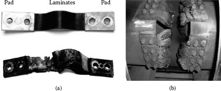
FIGURE 5.53
(a) Typical examples of flexible tinned copper connectors: intact and failed connector: (b) Example of failed flexible power connector.
TABLE 5.10
Resistance Measured in the Bulk of Connector Laminates, Across Cu–Sn Interface and Inside of Cu–Sn Intermetallic Phases
Sample |
Laminate Bulk (μΩ) |
Cu–Sn–Cu Interface μΩ |
Inside Cu–Sn Band (μΩ) |
Intact |
3 |
9.35 |
16.78 |
Damaged |
2.2 |
15.25 |
25.65 |
TABLE 5.11
Microhardness Measured in Copper Connector Laminates, within Tin Plating and Inside Cu–Sn Intermetallic Phases
Sample |
Laminate Bulk (μΩ) |
Cu–Sn–Cu Interface μΩ |
Inside Cu–Sn Band (μΩ) |
Intact |
100 |
6 |
345 |
Damaged |
70 |
– |
266 |
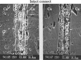
FIGURE 5.54
SEM micrographs and EDX spectra of intermetallic phases formed in intact and damaged flexible tinned copper connectors.
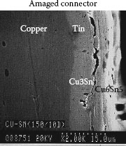
FIGURE 5.55
SEM micrograph of cracks at interface of intermetallic phases Cu3Sn and Cu6Sn5.
5.4.14 Stress Relaxation and Creep
Creep, or cold flow, occurs when a metal is subjected to a constant external force over a period of time. The rate of creep depends on stress and temperature and is higher for aluminum than for copper. Stress relaxation also depends on time, temperature and stress but, unlike creep, is not accompanied by dimensional changes. It occurs at high stress levels and is evidenced by a reduction in the contact pressure owing to changes in metallurgical structure. The change from elastic to plastic strain has the effect of significantly reducing the residual contact pressure in the joints, resulting in increased contact resistance, possibly to the point of failure. The loss of initial contact pressure can be accelerated at elevated temperatures, making a loss of contact area in a relatively short time. Hence, excessive conductor deformation and high stresses produced by certain connector systems with no way of providing residual mechanical loading to the contact interface cause accelerated stress relaxation and eventual failure of a joint.
The gist of the metallurgical state and temperature on the strain relaxation of aluminum and copper was investigated by Naybour and Farrell [71,99] and Atermo [100]. It was shown that, for electrical grade aluminum (EC-1350 grade), increasing the temperature and the amount of hardening augmented the rate of stress relaxation. It was also revealed that stress relaxation in hard-drawn EC-grade aluminum conductors was anisotropic, being much faster the transverse than in the longitudinal direction, and a great deal faster in hard-drawn than annealed wire. This is shown in Figure 5.56. Mounting evidence indicates that mechanical properties such as creep [101,102,103], stress relaxation [104,105,106], flow stress [107,108,109], metal forming [109,110,111,112,113,114,115,116,117], etc. can be significantly affected by the action of electric current. This so-called electroplasticity manifests itself in a spectacular increase in the ductility of a material. It is generally believed that the outcome is a result of the interaction between electrons and dislocations, although some controversy still exists regarding the precise nature of this electron-dislocation interaction. Even though there is a scarcity of data, I shall briefly review the nature of the effect of electric current on and provide some examples of this effect on stress relaxation and creep of some metals.
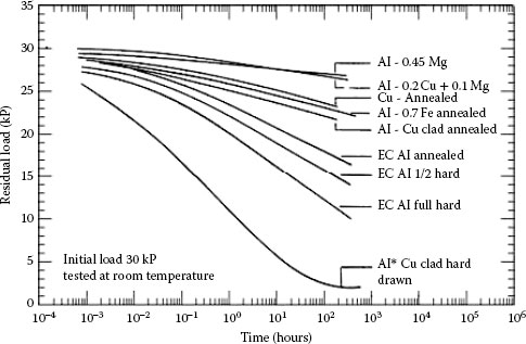
FIGURE 5.56
Effect of metallurgical state on the stress relaxation of aluminum.
5.4.15 Nature of the Effect of Electric Current
It is now well established that the electrons in a metal can exert a drag on dislocations, particularly those moving at high velocity at very low temperatures [94,95,96]. The electron drag coefficient Bew is given by
(5.23) |
where (f/l) is the force per unit length acting on the dislocation, ϑ is the resolved shear stress, b the Burgers vector and Vd the dislocation velocity. The electron drag coefficient Bew is of the order of 10−5 dyne/cm2 [103,104]. The interaction of moving electrons with the dislocations led Troitskii and Likhtman [115] to conclude that drift electrons can exert a force (“electron wind”) on dislocations and, therefore, that such a force should occur during the passage of an electric current through a metal when plastically deformed. A comprehensive reassessment of the extensive study of Russian scientists on the electroplastic effect is given by Trotsky and Spitsyn [104]. Theoretical considerations of the power exerted by drift electrons on dislocations are given in the papers by Kravchenko [116], Klimov et al. [117] and, more recently Roschupkin et al. [118]. The force is considered to be proportional to the difference between the drift electron velocity ve, and the dislocation velocity vd thus indicating that the electron wind force (few/l) is proportional to the current density,
(5.24) |
where ϑew is the stress acting on the dislocation owing to an electron wind, b the Burgers vector, Kew the electron force coefficient and J the current density. These theories give a different magnitude of the constant Kew which, in turn, is reflected in the value of the electron drag coefficient Bew given by:
(5.25) |
where e is the electron charge and n the electron density. The values of Bew predicted by Kravchenko for metals are of the order of 10−6dyn-s/cm2, those by Klimov et al. 10−6 to 10−4 dyn-s/cm2 and those by Roschupkin et al., 10−5 to 10−3 dyn-s/cm2. These values are all within the range of those measured experimentally for Bew although the theory of Klimov et al. gives the values in best accord with those most generally accepted [117,118].
In recent years, the electroplastic effect has been studied in the United States by Conrad and coworkers [119,120,121,122,123,124,125] who have carried out a series of investigations into the effects of single high-density DC pulses (~103 A/mm2 for ~60 μs duration) on the flow stress of a number of polycrystalline metals (Cu, Pb, Sn, Fe and Ti), representing a range of crystal structures and valences. The primary objectives of the work of this group were to determine:
• The magnitude of the drift electron-dislocation interaction which occurs with the application of a current pulse during plastic flow,
• The physical basis of this interaction.
In order to ascertain the magnitude of the electron-dislocation interaction, attention was given to separating the side effects of the current, such as Joule heating, pinch, skin and magnetostrictive effects. This was an indispensable first step since there was considerable skepticism [126] as to whether the electroplastic effect is a consequence of the electron-dislocation interaction. It has been argued that the observed changes in the mechanical properties such as flow stress, creep etc. are caused by a side effect of current such as Joule heating and pinch effect. However, Cao et al. [127] has clearly demonstrated that the observed changes in the mechanical properties cannot be explained in terms of the current side effects but rather are the result of the electron-dislocation interaction.
5.4.16 Effect of Electric Current on Stress Relaxation
Troitskii and co-workers [104] have used stress relaxation to study the electroplastic effect in a number of metals such as zinc, lead and cadmium under the influence of high-density (104 A/cm2) current pulses. The frequency of the pulsing current was 100 Hz and the pulse duration 65 μs. They found that the application of current increases the rate of stress relaxation and significantly affects its onset; see Figure 5.57. Figure 5.58a depicts stress relaxation Δτ with time with and without current. Figure 5.58b illustrates the rate of stress relaxation Δτ with and without current as a function of applied stress. Note that the onset of stress relaxation with and without electric current is different: it is significantly lower in the samples under the influence of electric current.
The mechanical properties of metals may also be tempted by low-density electric current as reported by Silveira and co-workers [128,129]. They have demonstrated that the rate of stress relaxation of polycrystalline Al and Cu near 0.5 Tm (where Tm is the melting temperature) can be increased with the application of a small (1.6 A/mm2 continuous AC or DC) current, the effect being greater for the DC current. The effect decreased with the number of current cycling times. Also, they found that the DC current altered the dislocation arrangement in the Cu specimens; partial destruction of the cell structure occurred even in the first relaxation cycle. No change in the dislocation structure was observed for Al. The effect of DC electric current on stress relaxation is shown in Figure 5.59. Braunovic [130] compared the stress relaxation of aluminum conductor wire at room temperature and low initial stress (20 N) under the influence of a low-density electric current (3 A/mm2) with that of a wire relaxing at higher temperature (150°C) and higher initial contact stress (260 N); see Figure 5.60. Here the relative force changes (Fi/Fo) versus time, where Fi is the contact force at the instant i and Fo. is the initial contact force. It is clear that the stress relaxation of an aluminum wire conductor at elevated temperature (150°C) and under current cycling conditions is similar. In other words, the initial contact force (Fi = 20 N) of a wire subjected to current cycling decreases at virtually the same rate as a wire subjected to stress relaxation at 150°C and higher initial stress Fo = 260 N. The observed effect of current cycling on stress relaxation cannot be justified in terms of the temperature effect alone, since the temperature rise produced by the passage of a low-density current through the wire conductor is merely 2°C–3°C.
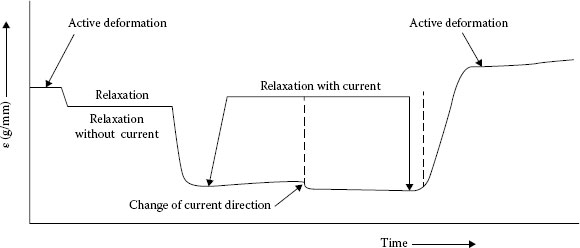
FIGURE 5.57
Stress relaxation of zinc crystal without and the intercept when the current was applied.

FIGURE 5.58
(a) Variation of stress relaxation with time with and without current; (b) variation of the rate of stress relaxation with applied stress for samples with and without current.
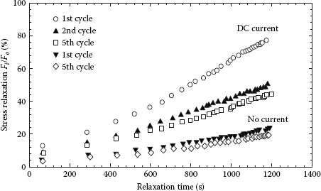
FIGURE 5.59
Effect of DC electric current on stress relaxation of copper.
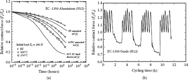
FIGURE 5.60
Stress relaxation of aluminum wire conductor (a) at room temperature (RT), 100°C and 150°C and 260 N initial load; (b) at room temperature under current cycling conditions and 20 N initial load.
One possible explanation is that current cycling causes thermal fatigue in aluminum wires which in turn reduces the overall durability of the material and thereby increases the rate of stress relaxation. Nevertheless, the temperature rise in the wire resulting from the current passage is of the order of 2°C–3°C, thus, insufficient to significantly change the properties or structure of the material (wire). Another possibility is that during cycling the contact zone, which is under compression, work-hardens as a result of increased contact stresses brought about by the thermal expansion of the wire. This, in turn, can augment the rate of stress relaxation, since it is well known that work hardening increases the rate of relaxation. Work-hardening of the contact zone may occur in response to the stresses generated by thermal expansion of the wire being high enough to cause localized yielding of the contacting asperities. Again this is unlikely because a temperature exceeding 2°C–3°C cannot generate sufficient thermal stresses to create significant work-hardening and, therefore, stress relaxation. An alternative explanation is that the observed effect of electric current on stress relaxation is associated with electroplasticity. The stress relaxation of a metal is generally associated with the arrangement, density and motion of dislocations and their interactions with other structural defects such as grain and subgrain boundaries, impurities, solutes, precipitates, etc. Hence, when the electric current passes across the wire, it will not only cause heating and, hence, the elaboration of the wire but also weaken the binding forces between dislocations and obstacles impeding dislocation motion, which otherwise cannot be overcome by thermal activation alone. As a result, nucleation and multiplication of dislocations will be alleviated this, in turn, will increase the density of mobile dislocations and alter their arrangement. Repeated passage (current cycling) of current through the wire will free more and more dislocations from pinning defects, enhance mobility and reduce their density in the material, thus, resulting in an increased rate of stress relaxation. It should be pointed out, however, that the effect of temperature on the processes involved was not excluded. However, because of the relatively low heating generated by the passing current, thermal activation alone is insufficient to significantly affect the dynamics of dislocation motion and their arrangements in the material.
The elementary processes of plastic deformation of metal during creep can be described by the phenomena related to the dislocation dynamics and viscous diffusion flow. The latter takes place at temperatures close to melting point. At medium temperatures and low applied stresses the creep rate gradually diminishes and vanishes, as reported by the logarithmic law
(5.26) |
where α and β are constants and εo is the initial deformation. The logarithmic law of creep is valid for metals and alloys with different types of crystal lattice at temperatures below (0.2–0.3) Tm, (Tm is the melting temperature) and can be used to study the mechanisms responsible for the rate of plastic deformation of a metal. At low temperatures, creep is dominated by the dislocation mechanism which reflects the combined action of thermal fluctuations and applied stress, resulting in an unimpeded motion of dislocations throughout the lattice. Figure 5.61 depicts the evolution of creep in power connections and accompanying processes occurring in the contact. The effect of electric current on creep in different metals has been studied extensively by Klypin [102] at a low-density DC current, (0.25 A/mm2) and different temperatures. It was demonstrated that the creep rate is significantly affected by the action of the electric current, the more so at lower creep rates and higher current densities (see Table 5.12). Increasing the number of current applications (cycles) was found to reduce the effect of electric current. A typical creep curve for copper tested at 400°C and a stress σ = 6 kgf/mm2 is shown in Figure 5.62. It is clear that when the current is applied the creep rate sharply increases.
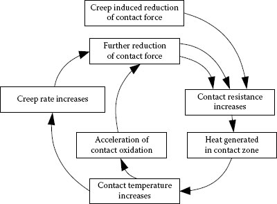
FIGURE 5.61
Schematic of creep evolution.
TABLE 5.12
Effect of DC Current (0.15 A/mm2) on the Creep of Different Materials
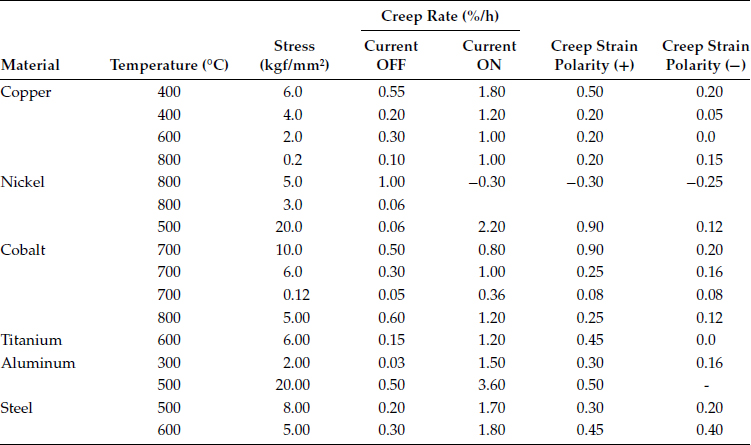
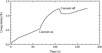
FIGURE 5.62
Effect of current on the creep of copper at 400°C and stress σ = 6 kgf/mm2. Note the change in creep rate when the current was switched ON and OFF.
The uninterrupted passage of current across the contact interface is influenced by many parameters such as the size and shape of the contact surface, pressure (torque) and contact resistance and protection against adverse environmental effects. Various palliative measures are used to ensure the continuous passage of current, A brief review of those most frequently used as follows. There are three basic ways for improving the contact performance: (a) development of new contact materials, coatings, and lubricants; (b) special techniques involving the structure and state of the interface; (c) improvement in contact design (Figure 5.63).
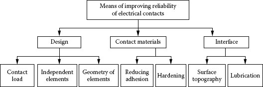
FIGURE 5.63
Main means of improving reliability of sliding contacts.
The size of the contact area is generally defined by the stiffness of the contacting members, applied force, and the rated current density. It should be sufficiently large to prevent the rise of the contact interface temperature under normal and emergency conditions. However, the contact temperature itself is not a critical parameter since it is an effect rather than a cause of the processes occurring in a joint, being a function of the current density, the geometrical dimensions of the contact, and the voltage drop across the contact. The contact temperature can exceed that in the bulk of a conductor or connector without causing electrical instability at the contact interface. On the other hand, the contact voltage cannot increase to even moderate values without causing the contact temperature to exceed that of the conductor or connector bulk temperature. It is therefore imperative that changes in the contact temperature and voltage with the connector operating time remain very small; ideally <10 mV. This requirement can be met providing the area of real contact is sufficiently large so that, despite initial and long-term deterioration, there is still a reserve of contact spots (a-spots) to ensure that the overheating conditions in the joints are not reached.
Practice and published experimental evidence has shown that mechanical abrasion (brushing) and lubrication of aluminum is the simplest and most efficient method of obtaining a large number of contact points [2,9]. In order to prevent oxidation of the exposed metal, brushing should be done with a contact aid compound (grease) applied to the contact surfaces. Serration of the connector contact surfaces is a very efficient method and most desirable when splicing conductors because it assures a large contact surface area between connector and conductor. Figure 5.64 shows the result of surface preparation and lubrication on the contact resistance of aluminum bolted joints [14,131].
In the event of a bolted joint, it has been indicated that current lines are distorted at the joints as a result of which, the resistance of even a perfectly made overlapping joint (no interface resistance) is higher than that of a bar of the same duration as the joint. This is known as “streamline effect” and is determined by the ratio between the overlap and busbar thickness. Figure 5.65 illustrates the action of current flowing through an overlapping busbars of uniform width (w), and thickness (t). Thus, the strip is shaped like a lapped joint but is void of contact surfaces along AB, except through part of its length AB where the thickness is 2t. A current (I), is passed through the busbar from end to end. The voltage drop is measured between A and B, and between B and C whereby distance AB to BC. Hence,
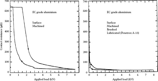
FIGURE 5.64
Effect of contact load and surface finish on the contact resistance of aluminum.
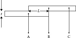
FIGURE 5.65
Schematic of an overlap joint without contact interface.
(5.27) |
where e is the streamline effect, R is the total resistance of a joint and RB is resistance of equal length of a busbar and is given as:
(5.28) |
Hence, the streamline effect e becomes a function of the ratio L/t, i.e
(5.29) |
Melsom and Booth et al. [132] have tested a number of different busbar combinations and obtained the results shown in Figure 5.66 which allows calculating the resistance caused by the streamline effect of a perfectly made overlap in relation to the resistance of an equal length of a single busbar. It appears that the streamline effect rapidly decreases until the overlap/thickness ratio reaches a value of 2 when its decrease is slowed down and practically stabilized upon passing a value of 6. In other words, upon reaching this value, the current distortion is minimized and the current lines become parallels. Consequently, the optimal overlap length in a bolted joint should be 5–7 times the busbar thickness. However, to meet all requirements, and for the sake of convenience, it is common practice to make overlaps equal to the width of the bus bar. Although this procedure is usually satisfactory for busbars of ordinary dimensions, it may not provide sufficient joint contact area on busbars that have a high thickness-to-width ratio. Hence, as a rule of thumb, the minimum overlap should be from 8 to 10 times the bar thickness. Furthermore, since the actual area of contact is much less than the total area of overlap, the determination of overlap on the basis of the width alone is reasonably safe practice only if the current density in the contact surface does not exceed 1/3 to 1/4 of the current density in the busbar cross section.
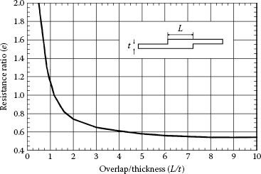
FIGURE 5.66
Effect of current distortion (“streamline effect”) on the contact resistance of an overlapping joint.
Donatti [133] has studied extensively bolted overlapping joints and found that the current tends to traverse the contact surface at the end points of the joint while the passage of current in the intermediate region is minimal. It was also demonstrated that when the two conductors of substantially different resistance values are in contact, the current will pass across the contact interface almost exclusively at the end of the better conductor, the remaining contact interface being almost inactive. Therefore, to reduce current density in the joints, it is useless to increase the contact surface by expanding its length, since this does not alter the current distribution to an appreciable extent. Rather, increasing the width of the contact surface was found to be more beneficial. Jackson has shown [14] that in a bolted joint, unless it is grown in a perfect manner, it is not possible to hold a uniform distribution of the current on the contact surface. Furthermore, it was also indicated that the current tends to traverse the contact surface at the end points of the joint while the intermediate area is used very little for the passage of current. This feature was exploited in the edge-shaped transition washer as seen in Figure 5.67 [134]. In the case of bolted connections, it was shown that the contact area can be increased by changing the busbar design. In other words, cutting the slots in the busbar in a manner as shown in Figure 5.68, the actual surface area of a joint can be increased by 1.5–1.7 times that of without slots. The contact resistance of a joint configuration without slots (A) is 30–40% inferior to that of (B), and is mechanically and electrically more stable under current cycling conditions [135]. The beneficial effect of sectioning the busbar is attributed to a uniform contact pressure distribution under the bolt and a larger contact area.

FIGURE 5.67
Pfisterer Transition washer (Elast contact disk) (a) Cross section of the busbars with the transitions washer showing the contact points, (b) Cross section of a transition washer, (c) Busbar contact surface showing the impressions left by the sharp edges of transition washer.
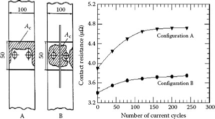
FIGURE 5.68
Contact area of a joint with slots (B) is 1.5 to 1.7 times larger than without slots.
This idea has been explored by Braunovic [136] in the case of high voltage (>700 kV) power connectors used for connecting stranded 4000 MCM conductors to a variety of power equipment at the sub-station site. The connectors used to be with intact current-carrying pads (no slots) and with pads modified by cutting slots seen in Figure 5.69.
The contact resistance was derived from the voltage drop measured between the potential leads positioned on the connector pads and busbars as shown in Figure 5.69. Although this figure depicts only the location of the voltage drop leads for the connectors with slots, the same system was used for the connectors without slots. The results in Table 5.13 show the mean values of joint contact resistance of connectors with four- and six-bolt configurations whereas Table 5.14 shows calculated composite radius of a-spot (ac) and composite contact area (Ac). To estimate the size of contact zone where conduction takes place, this zone can be envisaged as a large circular composite area comprising several discrete small areas (a-spots) with composite electrical resistance Rc (see Equation 5.7). Where ρ is the bulk resistivity of the connector aluminum alloy and ac is the composite radius. Hence, using the resistivity value ρ = 50 nΩ m typical for the aluminum commonly used for this type of connectors, the composite radius ac and real conducting area Ac; see Section 5.2.2. From the results presented in Tables 5.13 and 5.14 it is clear that sectioning the overlapping bolted joints combined with machining and lubricating the contact surface assured very pronounced enlargement of the actual conducting area and hence the lowest contact resistance. The slotted approach may prevent bolts from loosening with the improved contact area. On the other hand, connectors whose current-carrying parts (pads) were not given any surface treatment nor were sectioned, had extremely small conducting area and, thus, highest contact resistance.
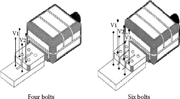
FIGURE 5.69
Schematic of the bolted joint configurations and positioning of the voltage probe leads for the contact resistance measurements.
TABLE 5.13
Mean Values of Joint Contact Resistance of Connectors with Four- and Six-Bolt Configuration
Condition |
No Slots |
With Slots |
Rs/Rns |
Four-Bolt Configuration |
|||
As received |
9.19 |
6.70 |
0.73 |
Brushed |
5.48 |
3.97 |
0.72 |
Brushed + Lubricated |
0.39 |
0.27 |
0.69 |
Six-Bolt Configuration |
|||
As received |
22.52 |
15.20 |
0.68 |
Machined |
2.74 |
1.55 |
0.56 |
Machined + Lubricated |
0.32 |
0.18 |
0.56 |
Rs—Contact resistance of contacting members with slots.
Rns—Contact resistance of contacting members without slots.
TABLE 5.14
Calculated Values of Joint Contact Resistance for Composite Radius (ac) of Composite Contact Area (Ac)
No Slots |
With Slots |
|||
Surface Finish |
ac |
Ac |
ac |
Ac |
Four-Bolt Configuration |
||||
As received |
0.27 |
0.23 |
0.37 |
0.43 |
Brushed |
0.46 |
0.66 |
0.63 |
1.25 |
Brushed + Lubricated |
6.29 |
1124.21 |
8.85 |
245.92 |
Six-Bolt Confuguration |
||||
As received |
0.11 |
0.04 |
0.16 |
0.08 |
Machined |
0.91 |
2.60 |
1.61 |
8.14 |
Machined + Lubricated |
7.72 |
187.14 |
13.89 |
605.81 |

FIGURE 5.70
Current lines of an idealized joint without (a) and with (b) slanted busbar ends.
Boychenko and Dzektster [135] have shown that the current distortion in the joint can be reduced by slanting the busbar ends at 45°; see Figure 5.70. Slanting the busbar ends will make the current flow across the joint more uniform. The initial contact resistance of bolted joints is 15% lower; see Figure 5.71. Also, the rate of contact resistance increase in a joint with slanted busbars (a) during current-cycling is 1.3–1.5 times slower (Figure 5.71) than that without slanted busbars (b). Lower contact resistance in a joint with slanted busbar is owing to uniform current distribution at the contact interface which eliminates localized overheating, thus improving the contact thermal stability. The contact resistance was derived from the voltage drop measured between the potential leads positioned on the connector pads and busbars as shown in Figure 5.69.
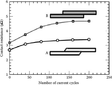
FIGURE 5.71
Effect of current-cycling on contact resistance of bolted joints with and without slanted busbar ends. Contact load 100 kN.
A well-designed connector should have adequate mechanical strength to maintain its mechanical integrity under normal and overload conductor operating conditions. It should also have sufficient contact pressure to maintain an ample contact area, thus allowing uninterrupted passage of current across the contacting interfaces. However, this pressure should never exceed elastic limits of the joint components since plastic deformation can increase stress relaxation and creep of the contacting members leading to eventual loss of a contact.
From the results presented in Tables 5.13 and 5.14 it is clear that connectors whose current carrying parts (pads) were not given any surface treatment nor were sectioned, had extremely small conducting area and, thus, highest contact resistance. The effect of contact load on the contact resistance of closed current-carrying copper contacts such as in the power disconnect switches, was investigated by Bron et al. [137]. The evolution of contact resistance of spherical copper contacts under 50 and 100 N contact force and a current of 1000 A was measured as a function of time. Note that the contact voltage of 100 mV is much greater than the 10 mV required to give a reliable contact joint. The results, shown in Figure 5.72 demonstrate clearly that increasing the contact load from 50 to 100 N extended the onset of the contact resistance increase, that is, the contact lifetime by 5 times. Furthermore, it was also shown that by increasing the applied contact force, the permissible temperature of electrical contacts can also be increased.
In the case of compression-type connectors, such as those used for splicing aluminum or copper conductors or terminating these at a particular electrical equipment such as transformer, disconnect switch etc. the force required to bring two or more conductors into contact and maintain this contact is provided through the deformation of a portion of the connector. This portion, usually referred to as the barrel or sleeve, is twisted in a predetermined shape and to a predetermined extent by a special tool, which may be a simple hand-actuated tool or a fully automatic power-operated machine. The deformation of the connector barrel is permanent so that the clamping force is maintained. The degree of compression is determined by looking at several factors. Mechanically, the compression force has to be sufficient to satisfy the mechanical requirement for the association. Electrically, the impedance of the connection has to be small enough so that the joint complies with the electrical demands. Simultaneously, the deformation of the connector sleeve has to be sufficient to sustain the required compression force for good. The force needed to execute this procedure has to be within the capabilities of the installation tool, allowing a sufficient margin of safety.
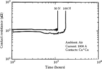
FIGURE 5.72
Evolution of contact resistance of spherical copper contacts with time under 50 and 100 N contact force.
There are definite relationships between the force necessary to achieve a given deformation or compression of any connector barrel, the conductor, and the installation die configuration. The same is true of the relationship of the degree of compression to the resulting electrical and mechanical characteristics of the connection. In establishing contact between a connector sleeve or cylinder, and a cable, deformation of the cylinder walls exerts pressure on the wire. The level of electrical conductivity of the connection is related to the amount of deformation. Put differently, in the initial stages of this deformation, the contact resistance is practically proportional to the deformation, that is, it decreases as the distortion increases. However, once the conductor is fixed firmly in the sleeve, the decrease in contact resistance levels off until no decrease is observed with further deformation. At this point a satisfactory electrical connection has been established.
The electrical and mechanical characteristics of a connector are equally important aspects that determine its reliability. Hence, to obtain a satisfactory electrical and mechanical connection, both characteristics have to be considered. Unlike electrical resistance which reaches a practically steady state with progressive deformation, the mechanical strength of a connection gradually decreases with increasing deformation which, in turn, will increase the rate of stress relaxation and creep of a connector. Closely related to this is the effect when dissimilar metals are used for the conductor and in the connector. Heating the joint by passing current through it creates a difference in the relative coefficient of expansion which may reduce the contact pressure, particularly if the conductor has a higher coefficient of expansion than the connector. There are other factors that can cause loss of mechanical load on the contacts. In a compression joint, a stranded conductor may not align itself perfectly during assembly and any subsequent realignment will make severe reductions in mechanical load. Furthermore, since aluminum is susceptible to creep, some functions will be under much greater strain than others and some stressed far beyond the yield point thus creating the conditions for extrusion to occur. Temperature will affect the rate of creep and, if increased far enough, will reduce the mechanical strength of a joint by annealing.
Experience has shown that a properly designed compression connector can exhibit a very good performance under high temperature cycling conditions. This is owing to the mechanical restraint provided by the structural configuration of the connector and the nearly complete enclosure of the conductor, which partially seals the contact area from adverse effects of the environment. The effect of conductor hardness on the quality of different compression-type connector joints has been investigated by Jesvold et al. [138]. The tests, conducted according to standard International Electrotechnical Commission IEC 1238-1 on both soft and hard conductors, have demonstrated that the conductor hardness and the extent of the mechanical deformations created during assembly strongly influence the quality of a compression joint. It was demonstrated that reliable connections between soft (annealed) aluminum conductors can be obtained simply by using connectors that mechanically deform the strands so heavily that the strand hardness becomes comparable with that of hard-drawn conductors. Braunovic and Dang [139] made a comparative evaluation of different compression-type underground connections. The connectors were evaluated according to their performance under current-cycling conditions. The connectors evaluated were compression sleeve and stepped-deep indentation connectors as shown in Figure 5.73. The results of the current-cycling tests in Figure 5.74 show changes in the maximum and minimum temperature and normalized resistance with a number of current cycles. The data were obtained by averaging the readings from the four connectors of the same kind under tests. The normalized resistance with respect to 20°C was obtained using the expression
(5.30) |
where R(T) is the contact resistance measured at temperature T. The most significant feature of these events is that the performance under current-cycling conditions is significantly affected by the type of connection. This is mainly reflected in the changes in contact resistance with current-cycling time whereas the connector temperature was affected to a lesser degree. The stepped-deep indentation connector had the most stable performance: both the temperature and contact resistance remained practically untouched by the current-cycling. However, the compression sleeve connector showed a different tendency: although its temperature remained fairly stable, its contact resistance was greatly affected by current-cycling. The increase in the contact resistance was 13%, thus exceeding the acceptance resistance criterion limit [140,141,142].
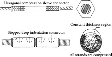
FIGURE 5.73
Schematic of compression sleeve and stepped deep indentation connectors.
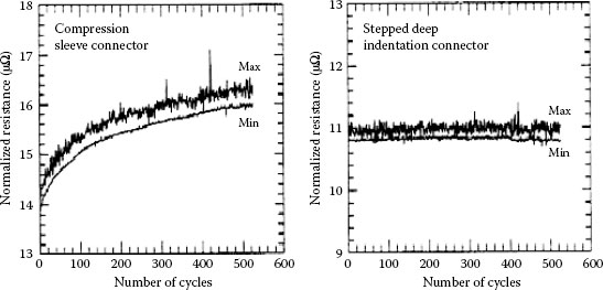
FIGURE 5.74
Effect of current-cycling on the normalized contact resistance of compression sleeve and stepped deep indentation connectors.
There are several plausible explanations for the observed inferior performance of compression sleeve connectors. One possibility is that the mechanical properties (hardness in particular) of the connector and the conductor are different, which, during mechanical deformation, will cause both connector and conductor to work-harden at different rates. As a consequence, during current-cycling, both connector and conductor will relax at different paces. The net result is a progressive loss of contact load and a gradual increase in the joint resistance, although the bulk temperature may not have been moved to the point of bankruptcy. This is because the contact resistance is more sensitive to the changes occurring at the a-spots than to the bulk connector temperature. Another possibility is that current-cycling produces thermal fatigue of the a-spots. The magnitude of the thermal strains induced will depend on the contact spot temperature rise and the coefficient of thermal expansion of the joint materials. The magnitude of the corresponding stresses generated by the thermal strains is influenced by the reduction in the yield strength with temperature as well as by structural changes that can affect ductility and resistance to thermal shock.
It is also possible that the design of the compression sleeve connector does not provide sufficient mechanical deformation to bring down the initial contact resistance to a level where it is independent of the deformation applied. Indeed, the initial contact resistance of compression sleeve connectors is about 30% higher than that of the stepped-deep indentation ones as pictured in Figure 5.73. Put differently, it is the ability of the connector contact surface to envelope the conductor and provides solid support which is important. It seems that in the compression sleeve connection this may not have been achieved, resulting in a greater tendency for substantial relaxation from the slippage of strands subsequent to installation. The advantages and disadvantages of compression type connectors are summarized in Table 5.15.
For bolted joints the contact resistance in clean contacts is determined by the resistivity of the contact members, the contact area and distribution of the conducting spots in the interface between the contact members. The area and distribution of the conducting spots are generally determined by the surface finish and the magnitude of the applied force and the manner in which it is applied. Therefore, the quantitative application of laboratory data to an actual bolted joint is possible only in so far as the laboratory conditions duplicate the activity of the fastener. Every fastener (bolt with washers or clamp assembly) produces conducting spots that are allotted according to the characteristics of the fastener and the busbar.
TABLE 5.15
Summary of Advantages and Disadvantages of Compression-Type Connectors
Advantages |
Disadvantages |
|
Low cost, relatively reliable performance, use of recommended tools and/or dies removes the human element during installation. Connector construction provides better conductor encirclement while retained oxide inhibiting compound protects the contact area from the atmosphere, thus assuring a maintenance free connection. High localized and consistent forces imparted by the installation tool break down the oxides and establish contact points (a-spots) for reduced contact resistance, thus providing electrically and mechanically sound connection. The softness of compression connector material relative to the conductor prevents spring back and contact separation. Due to their geometry, compression connectors are considerably easier to insulate or tape than mechanical connectors. These connectors are most suitable in areas of wind, vibration, ice build-up and other stress-associated tension applications. Require no soldering. Require no special tools or skill to operator. Work at higher pressures and with toxic gases. Useful when occasional disassembly is required for maintenance. They can be assembled and disassembled without affecting the joint integrity. Can be used where heat source (soldering) is prohibited. |
Proper installation tooling for a compression system program involves potentially high capital investments due to a large variety of different types of compression tooling to select from. Accurate die and tool selection is essential for proper installation of a compression connection. Due to the need for specific tools and dies to install a compression connection, installers must be trained how to use the proper techniques and maintain these tools. In some compression connections, manually operated tools require greater physical exertion to install, thus when installing numerous connections, installers can become fatigued and possibly not complete the specified number of crimps. Not as robust as soldering fittings. Should be used in applications where fitting will not be disturbed and subjected to flexing or bending. Compression fittings are much more sensitive to dynamic stresses. They are also bulkier and less aesthetically pleasing than a neatly soldered joint. The use of a special tool is disadvantage in any situation, likewise, not having to use a special tool is an advantage. |
The relationship between the contact resistance (Rc) and the applied force (F) can be described by;
(5.31) |