
Materials, Coatings, and Platings
Feltem
CONTENTS
8.1.2 Requirements of Contact Finishes and Coatings
8.2.2 Electrodeposits and Electroless Deposits
8.2.2.3 Classification of Platings
8.2.3 Contact Finishes Produced by Non-Chemical Methods
8.2.4 Metal-in-Elastomer Materials
8.3 Properties Related to Porosity
8.3.3 Relationships Between Porosity, Thickness of Finish, and Substrate Roughness
8.3.4 Effect of Underplatings, Flash Coatings, and Strikes on the Porosity of Electrodeposits
8.3.5 Reduction in the Chemical Reactivity of Finishes by the Use of Underplates
8.4 Metallurgical and Structural Properties
8.5 Physical and Mechanical Properties
8.5.1 Characteristics of Layered Systems
This chapter concerns finishes and coatings that are used on the contacts of separable electronic connectors. Because of the relatively small size of these connectors it is difficult to design their contact springs in such a way as to supply high normal loads that could facilitate the fracture and displacement of insulating oxide and corrosion films on uncoated base metal substrates. It is, therefore, necessary to modify the contact metals so as to be able consistently provide low contact resistance during the lifetime of the connector. This is achieved with suitable contact finishes and coatings. The terms “finishes” and “coatings” mean any material that is applied to a substrate. Thus, it includes electrolytic and electroless deposits, clad metals, fused metal layers, weldments, and materials from physical processes such as ion implantation and vacuum evaporation. These terms also embrace lubricants and chemical treatments for inhibiting the formation of corrosion and tarnish films on separable contact surfaces.
8.1.2 Requirements of Contact Finishes and Coatings
The purpose of a contact finish is to upgrade the contact substrate’s properties such as its oxidation, tarnish, and corrosion resistance, electrical conductivity, durability, frictional properties, and solderability. In order to be useful, finishes and coatings should not have concomitant deleterious properties. For example, while silver-plated contacts resist degradation by fretting corrosion, they can be tarnished in mildly polluted environments [1]. The proper selection of contact finishes and coatings requires an understanding of the engineering requirements of the application. Additional considerations include material cost and availability, and ease of manufacture.
Common terms that describe coatings and substrates are given in Table 8.1.
Although several finishes and surface treatments have been evaluated for connector contacts, only a few are widely used. These include some multilayered electrodeposits, electroless deposits, claddings, and fluids besides greases on the contact metal or as secondary coatings on metal finishes.
Contact or Basis Metal |
Substrate |
Base metal |
Non-noble metal |
Finish |
Layer(s) on substrate |
Plating |
Electro- or electroless deposit |
Underplate |
A layer under the top plating |
Subplate(s) |
When there are more than two layers of plating |
Strike |
Thin electrodeposit between two thicker electrodeposits or an electrodeposit and the substrate |
Flash |
Thin electrodeposit at outer surface |
Cladding |
Rolled metal, metallurgically bonded to the substrate |
Liner |
Clad metal underlayer (usually nickel) between surface layer of metal and the substrate; also called interliner |
Claddings are made by compressing two or more metals at a very high force which creates metallurgical bonds at their interfaces and elongates the composite. The top layers are usually a noble metal on a nickel liner, and most substrates are copper alloy spring metals such as 98.1 wt% Cu, 1.9 wt% Be (Unified Numbering System [UNS] designation 17200); 94.8 wt% Cu, 5.0 wt% Sn, 0.19 wt% P (phosphor bronze, C51000) and 88.2 wt% Cu, 9.5 wt% Ni, 2.3 wt% Sn (C72500); see Chapter 24, Table 24.9. With a flat stock, the cladding is obtained by squeezing between rolls (see Chapter 17, Section 17.5). Clad inlays are produced by first skiving a groove in the substrate into which a strip of the precious contact metal on the nickel liner is placed and then rolled. For clad wires of circular or other shapes, the substrate in the form of a rod is pressed into the hollow tubes of nickel and the noble metal, which then is drawn through a die. Heat is released during reduction which facilitates interdiffusion at the layer interfaces. Work-hardening occurs, and so annealing in an inert atmosphere, followed by further reduction, may be needed to obtain the desired thickness. Sheet clad metal is, then, slit to width and is the raw material for stamping and forming the contact. The amount of required precious metal is minimized by selectively locating it on the substrate so to achieve the ideal “contact engineering surface.” Excess material, cut away in the stamping, is reclaimed. Thicknesses of the noble metal in the inlay for contacts typically range at 0.75–5 μm. Multilayer inlays can also be obtained. The nickel liner is usually several micrometers thick.
Common claddings include pure gold, 75Au25Ag, palladium, 80Pd20Ni, 60Pd40Ag, 69Au25Ag6Pt, and DG R-156 (diffused gold 60Pd40Ag). DG R-156 is made by partially diffusing a golden top layer on palladium–silver to give a resulting surface composition of about 80% gold [2]. The ratio of thicknesses of the gold and 60Pd40Ag in the starting material is about 1/10, although different ratios of the metals are sometimes used [3]. Pure palladium and palladium–nickel alloys with a diffused gold surface have also been made.
Round “dots” of solid noble contact metals are produced by welding the end of a wire to the substrate, and then clipping, and coining. The weldment is usually applied to a contact spring. Pure gold, gold alloys hardened with 25%–30% silver, and palladium have been used. Typical weldment thicknesses are 25–75 μm.
Fusion coatings are made by contacting the sheet substrate with molten tin after prior treatment to remove superficial oxides. Thickness is controlled by wiping the molten surface with blades or with blowing air. Typical coating thicknesses are 2.5–10 μm. The sheet metal is then stamped and formed to the finished part. Fusion-coated contacts are attractive because of their low cost.
8.2.2 Electrodeposits and Electroless Deposits
Electrodeposits are produced by the electrolysis of a solution containing ionic species with electrons supplied by an external power source. Electroless plating involves the use of a chemical reducing agent in solution which provides the electrons for converting metal ions to the elemental form. This process requires a catalytic surface, and once plating is initiated, the metal being deposited catalyzes the process further. Electroless nickel contains 5%–10% phosphorus.
Important contact finishes are listed in Table 8.2 together with other deposits that are no longer used in significant amounts. The most common finishes are silver, tin, nickel and hard golds (golds that contain about 0.1%–0.5% cobalt, nickel, or iron and plated from acid or neutral cyanide chemistries). Gold flashes deposited on to nickel, palladium and 80Pd20Ni alloy are cheaper replacements for hard golds in many applications.
Table 8.3 describes the thicknesses of common contact platings in electronic connectors.
TABLE 8.2
Some Electronic Connector Contact Finishesa: Electrolytic and Electroless Deposits
In Current Commercial Use |
Sn |
Hard golds |
Gold flash/80Pd20Nib |
Gold flash/Pdb |
Ag |
Au, pure |
Rh |
Ni & electroless Ni (Contains 5–10% P) with no noble top layer |
Obsolete |
Pd |
65Sn35Ni |
Gold flash/65Sn35Nib |
AuAg (max. 5% (Ag) alkaline cyanide process |
AuCuCd alloy, 18 karat cyanide process |
Hard gold on an Ag underplateb |
AuAg on an Ag underplate |
Sn–Pb alloys (usually containing about 40–60% or 5–10% Pb)c |
a Usually on a Ni (sometimes electroless Ni or electrolytic NiP) underplate. Supplementary lubricant coatings are common.
b The flash is usually hard gold, although pure gold is sometimes used.
c Pb is now considered a hazardous material and is banned for general use
TABLE 8.3
Nominal Plating Thicknesses
Hard golds |
1.25 μm; military, aggressive environments, high-reliability, life-threatening applications 0.75 μm; common industrial applications < 0.75 μm; short-lived products, primarily for consumer applications in benign or protected environments, and where durability requirements are modest. |
Palladium and 80Pd20Ni alloy |
Generally used with a gold flash. 0.75–1.25 μm; normal industrial applications where high levels of durability are required. |
Tin |
2.5–5 μm; non-critical applications; some usage below 2.5 μm, but not recommended. |
Nickel |
5 μm; where relatively high forces can be used; protected environments; battery contacts 1.25–2.5 μm; common as an underplate. |
Silver |
5–15 μm; when plated on copper, 5 μm results in a mixed Cu/Ag chemistry. At 15 μm Ag chemistry dominates |
TABLE 8.4
Electrodeposit Hardness (× 102 Nmm−2)
Tin |
0.8–3.5 |
Gold, pure |
4–9 |
Silver |
4–18.5 |
Hard golds |
16–22 |
Palladium |
20–30 |
80Pd20Ni |
35–55 |
Nickel |
25–55 |
Ruthenium |
80–100 |
Typical values for these electrodeposits used in electric contacts are at the mid-range.
The hardness of platings is generally slightly greater than that of wrought metals having the same composition. When the layer is thinner than about 10–20 μm, its intrinsic hardness is determined on polished cross-sections by metallography using microhardness indenters, such as a Knoop diamond at 0.25 N, or optical microscopy. Smaller indentation loads and measurement of the indentation at high magnification with a scanning electron microscope is sometimes employed for very thin deposits. The hardness of a multilayered contact normal to its surface is different from the bulk hardness of the finish (see Sections 1.3, 8.5.2 and Table 24.1C). Table 8.4 gives the intrinsic hardness of common electrodeposits.
8.2.2.3 Classification of Platings
A brief overview of the properties of the most common electrodeposited coatings is given here.
They are the best choice for the finish in most applications. As they have noble metal properties, they are less prone to formation of films than any other metal. They are the most “forgiving” finish available. However, they are subject to pore corrosion and surface film creep in aggressive environments when in contact with certain base metals. They are also difficult to form without cracking because of their low ductility.
8.2.2.3.2 Palladium and Palladium–Nickel Alloy
These metals form tarnish films and frictional polymers in polluted environments, which can be minimized with a gold flash. Although previously these metals cost about one-third to one-half the cost of gold of the same thickness, it is no longer the case. Thus, the tendency to use them in place of gold in some applications has lessened. The gold flash reduces the wear due to adhesives, and instability of the contact resistance from fretting of the palladium and palladium–nickel, but its durability may be limited unless the connection is appropriately lubricated [4]. Now, there are several improved techniques available for the process of plating Pd–Ni to a substrate [5,6]. Older, now obsolete, palladium plating processes tend to give microcracked finishes. Now that the price of palladium has risen, it is no longer being considered as a plating material for connectors.
With the continued rise in the price of gold, efforts are on in exploring the suitability of silver as a substitute plating material [7]. Although it is only a “near noble” metal, its much lower cost and excellent electrical and thermal characteristics make it a potentially attractive alternative to gold. Unlike gold, silver is susceptible to forming tarnish films of Ag2S and AgCl if exposed to ambients where sulfur or chlorine compounds are present (e.g., H2S, PVC packaging and even some cardboard packaging). Thus, a gold plate cannot be replaced straightway with a silver one. There are several points of care required. Myers [7] has considered the performance of a silver plate as replacement for gold using a 2.4-μm silver layer over a 1.7-μm nickel underplate on a rolled phosphor bronze strip substrate. She has found that a coating of a palliative or inhibitor compound such as Evabrite [8] provides some long-term protection from tarnishing under normal temperatures and humidities. The study results in a number of conclusions:
1. For storage and shipping, silver-plated connectors should be placed in a sulfur absorbent packaging. PVC packaging must be avoided as it can result in severe chloride corrosion of the silver. Also some cardboard packagings can contribute to formation of sulfides.
2. Silver requires a higher contact force than gold in order to break through any light tarnish film that may be present. It is also useful to have a wiping action when making contact. Thus, this could well place a limit on the number of mating cycles for silver-plated connectors.
3. The higher contact force and the greater coefficient of friction increase the insertion force required for silver-plated connectors.
4. There are two other concerns regarding the use of silver in plating. The first is electromigration ([9] and also see Chapter 2, Section 2.4.3) and the second is the formation of silver whiskers from tarnish layers, that is Ag2S (see Section 8.4.4). Both of these effects can result in failure especially where separated conductors are closely spaced.
Nickel is inexpensive, but is covered with a tough oxide that must be broken to make a good electrical contact. It requires a relatively high force for forming a reliable connection. It is resistant to corrosion except at high humidity conditions; further, when in contact with more noble metals (gold, silver, and so on), it may corrode severely. It is susceptible to fretting corrosion, but there is some evidence that this can be lessened for up to 10,000 cycles [10]. It can also be used with care in highly polluting industrial environments [11].
8.2.2.3.5 Tin
Tin coatings are relatively inexpensive, but not durable. They are prone to degradation due to fretting corrosion, especially when mated to other metals. Pure tin can form “whiskers” (see Section 8.4.3). Degradation is also possible due to formation of intermetallic compounds. While lead is added to prevent the growth of whiskers, it cannot be used as a coating due to its hazardous nature; that is, the use of tin–lead alloys has mostly disappeared from electrical contacts and solders, because of the RoHS (Restrictions of Hazardous Substances) regulations.
8.2.2.3.6 Intrinsic Polymers in Hard Gold Plates
The unique properties of hard golds are attributable to the metalloorganic solids that are termed “intrinsic polymers” [12]. These polymers are fine particulates, of the order of tens of angstroms, and are also deposited (co-deposited) primarily at grain boundaries [13]. Some polymeric material may be present as larger islands in the deposit [14]. The solids have been hypothesized to be potassium–cobalt (or nickel)–gold–cyanide complexes [15]. Part of the co-deposited metal is present in the gold. The density of hard gold is 5%–10% less than that of pure gold. Unusual properties of hard gold compared to wrought gold that contains a small (< 1%) amount of alloy metals, are its high hardness, low ductility, and superior resistance to wear due to adhesion.
Many other electrodeposited connector contact finishes have been described and some have been used commercially to a limited degree. A few examples are “pure” hard golds (24-carat) hard gold [16] and additive-free hard gold [17], golds containing arsenic, cadmium, or other metals from sulfite-plating solution chemistries [18], ruthenium with and without a gold flash [19], gold-flashed PdCo [20] and PdNiCo [21] alloys, heat-treated pure gold plate on solid nickel or a thick nickel underplate [22], and heat-treated polyacrylonitrile on nickel [23]. The absence of compelling technical advantages, process limitations, inadequate deposit characterization, the highly proprietary aspects of the finishes, the lack of industry standards, and the absence of suppliers who are able to provide them have been impediments to their widespread acceptance.
8.2.3 Contact Finishes Produced by Non-chemical Methods
Some connector contact finishes obtained by physical processes, besides cladding, have been evaluated to a limited extent. These include ion-plated and vapor-deposited silver, sputtered gold, silver, and silver–tin alloy [24], flame-sprayed tungsten carbide and other “conductive hard metals” [25], titanium nitride [26], and gold or palladium [27] or silver [28] implanted with nitrogen, boron [29], or other elements [30]. The high cost of the equipment required to prepare these finishes on contact substrates has been the most serious impediment to their commercial use. However, there seems to be a growing interest for using a suitable deposition technology for making silver coatings to replace gold [31].
8.2.4 Metal-in-Elastomer Materials
Metal-in-elastomer materials consist of metallic conductors, embedded in sheet elastomers, that are oriented in the Z (thickness) direction [32,33]. The conductive elements are gold-plated or silver-plated tiny metal spheres or fine wires that protrude from the surface. The elastomer provides insulation in the X–Y plane and is usually a silicone rubber. These materials are used to interconnect components such as fine line printed circuit boards. They have the advantage of not requiring precise orientation, and are made as part of a connector structure involving clamps and fixtures for holding the elements of the system together.
Hard golds, tin, gold-flashed palladium and palladium–nickel alloys, electrolytic and electroless nickel, and some clad noble metals constitute most of the contact finishes for commercial electronic connectors. There is an increasing use of silver (for its high conductivity and lower cost than gold) in some connector applications. The use of these lower cost materials is far more common in higher voltage/higher current circuits (see Chapter 5).
In many cases, the designer has the choice of specifying either clad or plated contact materials for his product. The comparative properties and fabrication characteristics of these metals can be summarized as follows:
1. Spring materials with a clad noble metal or tin layer can be fabricated into the finished product without further processing of the plating.
2. Certain materials can be obtained only by cladding, that is, DG R-156, 69Au25Ag6Pt, while others, for example, hard golds and electroless nickel, are unique platings.
3. Both cladding (inlay, top-lay, edge-lay) and electrodeposition processes can selectively locate a material on the contact.
4. Clad metals are ductile and lend themselves to forming. A hard gold, when thicker than a flash, is prone to cracking during fabrication. Some electrodeposits, such as tin, are sufficiently ductile to permit forming after plating. Hollow tubes can more readily be made with a finish of the clad stock on the inner surface than by plating the formed part.
5. Plated layers can be made thinner than claddings. It is usually more economical to clad when a large thickness is required.
6. Hard golds have an unique ability to resist adhesive wear compared to clad metals. A gold flash can be put on a clad metal to improve its resistance to wear due to adhesion.
7. There are relatively few fabricators of clad contact metals, despite the fact that processing technology, although primitive by today’s standards, has been known since the early 1960s. Plating is much more deeply entrenched, having been practiced for some metals since long before the birth of the electronic connector. There are numerous captive and independent plating organizations that are supplied by many chemical and process equipment firms. The scientific and trade literature on electrodeposition is large. Organic lubricants have been used to some extent in conjunction with metallic finishes for separable contracts. They are discussed in Chapters 3, 5, and 7.
8.3 Properties Related to Porosity
The selection of contact finishes for electronic connectors is based on a number of factors. The main technical considerations are the chemical, metallurgical, physical, and mechanical properties, and the commercial aspect relates to the feasibility of production. When cost is a major consideration, precious metals are used in small thicknesses and selectively placed on the substrate. Porosity in the finish and the migration (creep) of surface films over the precious metal from adjacent base metal in aggressive environments may become a problem (see also Sections 2.4.4 and 3.2.4).
A few base metal finishes are suitable for connector contacts in applications that have low current. Thick, relatively pore-free, tin coatings are an exception because of the fairly low reactivity, proneness to deformation which facilitates the disruption of surface films, and solderability. However, poor resistance to sliding wear, susceptibility to fretting corrosion, formation of intermetallic compounds, and whiskering of pure tin can degrade contact reliability. Even some precious and semi-noble finishes, like silver and the platinum group metals, can acquire insulating films by catalytic effects or by sulfiding, and are therefore severely limited. Considerations involved in the selection of finishes are the subject of this section. Creep and electromigration are discussed in Chapters 2 and 3. Catalytic effects, or frictional polymerization, are described in Chapter 7 as part of the problems of fretting.
Pores are defects in a coating which expose the underlying metal, the underplate, or the underplate and substrate ([34,35]; see Sections 2.4.3 and 3.2.4.6). They may be intrinsic in the layer, that is, present in the coating when it is made. Subsequent forming of the coated metal can also produce cracks in the finish. Wear from service of the component may result in penetration of the layer. Intrinsic porosity in electrodeposited coatings originates in occluded foreign materials such as oxide particles in the substrate surface, even after rigorous cleaning. It has been found that these substances may be layered in “zones” in the substrate and appear during etching. Particulates from inadequately filtered plating solutions may co-deposit and cause porosity. Scratches on the substrate are often the sites of pores in the deposit. Co-deposited particulate material in the coating’s surface may cause localized corrosion and degradations due to pore formation. Clad metal finishes likewise may become porous if dust is embedded in the surface during fabrication. High spots on a rough substrate may penetrate the clad layer during rolling or drawing and create pores.
Except for base metal coatings that are so thick that porosity is virtually absent, porosity testing is quite common. Its main objectives are to:
1. Determine the quality of the finish—how well it protects the contact from exposure to a potentially aggressive atmosphere.
2. Assess the effects of mechanical processing: stamping, forming, chamfering of the edge contacts of a printed circuit board.
3. Determine the effects of wear due to engagement.
4. Assist in the development of new coating processes.
5. Facilitate control of the coating process because:
a. Porosity is easy to determine.
b. Porosity is a sensitive indicator of the stability of the process.
6. Satisfy customer requirements of excluding porosity in a contact finish.
Many porosity tests have been devised. Nearly all involve exposure of the contact to aggressive chemical reagents which develop corrosion “decorations” at the defect sites. The requirements of porosity tests, therefore, are that they:
• Should be fast—minutes to hours in duration
• Should be easy, and of low cost
• Should be reproducible
• Should be standardized (ASTM and other organizations are active in standardization)
• Should be non-reactive with the finish
• Should enable pores to be counted or sized
• Should have good pore delineation; minimal spreading of decoration (little tendency to “halo” formation)
• Should have the tendency for minimal formation of hygroscopic corrosion solids (sample can be heated after gas exposure to eliminate moisture).
Among the most useful porosity tests for precious metal coatings are the following:
Test Method |
ASTM |
Nitric acid vapor |
B735 |
Sulfur dioxide (sulfurous acid method) |
B799 |
Flowers-of-sulfur |
B809 |
Paper electrography |
B741 |
The gas exposure tests are suitable for contacts of any size and shape. Paper electrography is limited to flat or gently curved substrates, but provides a permanent record of defects in the surface. Method B735 should not be employed for palladium-based finishes because nitric acid vapor attacks palladium. Method B799 is suitable for all common precious metal coatings except alloys that are high in base metal content. Immersion in ammonium polysulfide solution after a gas exposure can darken corrosion solids to make them more visible. The decorations, whether corrosion solids or colored spots on paper in electrography, are not the actual sizes of the defects, but are considerably larger. Since porosity is usually of microscopic dimensions, magnification—produced by the spreading or growth of the corrosion material—is necessary in order to facilitate observation of the pores. The magnification factor diminishes with increasing size of the defect. Porosity tests are destructive since the contact cannot be used after testing. A model of pore corrosion development for a 1.18-μm gold plate over copper with a roughness of 262 nm shows a general agreement with experimental data [36]. However, the measured electrical contact resistance values show a bias towards the larger bloom not taken into account by the model.
The maximum acceptable number of pores in a separable connector contact finish of a precious metal depends on the severity of the service environment, shielding inherent in the connector structure, the ability of the contact to displace insulating corrosion products during engagement, the criterion for circuit failure, and the reliability that is required in the application. A typical specification for a high-reliability, 20-year-life, 40-contact connector limits the numbers of pores in a sample lot of contacts to no more than two to four on the engineering surface, that is, 0.05–0.1 defects per contact. This requirement can usually be satisfied with a 1-μm thick plated or clad precious metal coating that is made by state-of-the-art manufacturing processes.
8.3.3 Relationships Between Porosity, Thickness of Finish, and Substrate Roughness
The porosity of a finish diminishes with increasing thickness. Porosity rises with increasing substrate roughness. Typical data are given in Figure 8.1 for electrodeposited gold on copper substrates that were abraded with metallographic papers before plating. The sensitivity of porosity to roughness is often overlooked by connector designers and manufacturers. This is unfortunate because, besides porosity, a contact’s durability is degraded as the roughness is increased.
The reason for the dependence of porosity on substrate topography is that thickness (as given in Figure 8.1) is generally determined by X-ray fluorescence because it is non-destructive, rapid, and inexpensive. However, this method actually determines the mass of metal on the surface being studied, not thickness. Since a rough surface has a larger area, the real thickness of the coating will be less than if the surface were smooth. The sections in Figure 8.2 [37] show contacts having the same mass of deposit (identical “apparent” thickness). In addition, a non-uniform thickness distribution of plating on the surface (compare Figures 8.2a and b) exaggerates the discrepancy between the actual and apparent thicknesses. A larger surface will have a larger total number of defects, such as occluded impurities, which also contributes to porosity in the plating.
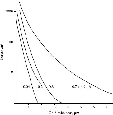
FIGURE 8.1
Dependence of porosity on deposit thickness and substrate roughness [38] (CLA–center line average); pure gold with 1.5 μm nickel underplate deposited on copper coupons that were abraded with metallographic papers prior to plating; porosity determined by electrography.
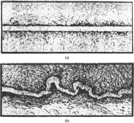
FIGURE 8.2
Metallographic sections of gold plated on copper [38]; nominal deposit thickness, 2.9 μm: (a) Smooth substrate, 0.04 μm CLA (b) Rough substrate, 0.7 μm CLA.
An example of the effect of substrate roughness on the reliability of contacts is given in Figure 8.3 [38]. Copper coupons plated with gold and a nickel underplate were exposed to a sulfur dioxide-containing corrosive atmosphere, and probed at a series of loads according to ASTM B667, “Standard Practice for Construction and Use of a Probe for Measuring Electrical Contact Resistance.” A doubling of the initial contact resistance was considered to be evidence of formation of a corrosion film and constituted a failure. It is clear that the rougher the substrate surface, the less reliable was the contact, especially at low loads. Apparently, the enhanced ability of a rough surface to penetrate contamination and to lower contact resistance was insufficient to overcome the larger amount of corrosion products.
8.3.4 Effect of Underplatings, Flash Coatings, and Strikes on the Porosity of Electrodeposits
In general, underplating, flash coatings, and strikes can lower the effect of a deposit’s porosity. These layers serve additional functions. For example, in a nickel underplate, they increase the composite hardness of the deposit thereby reducing sliding wear. Strike coatings can improve the adhesion of layers. A gold flash can serve a lubricating function in some systems.
The effect of these additional layers on porosity of the deposits has been attributed to their ability to cover defects in the surface of the substrate and thereby provide a better surface for plating. As these layers are better for closing the pores as compared to the original deposit as they thicken during plating, a given total thickness of a multilayered material will be less porous than a single layer of the same thickness. The multilayers consist of one or more of the strike, underplate, and flash, along with the deposit. A pore at the surface of a layer, that is, the underplate, is considered to be a defect. This analysis assumes that a pore in the deposit is smaller than an original defect of the underlying metal. Even so, a nickel-flashed underplate, a 0.46-μm gold top layer exposed to air for 15 months still shows considerable pore corrosion [39].
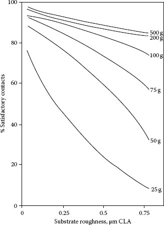
FIGURE 8.3
Effect of substrate roughness on contact reliability of plated contacts after exposure to a corrosive atmosphere: 1% SO2, 95% RH, 45°C, 120 hours [39]; pure gold plate (1 μm) on nickel underplate (2.5 μm); copper substrate. Probed according to ASTM B667. Criterion of satisfactory contact: contact resistance, not in excess of 1 mΩ.
8.3.5 Reduction in the Chemical Reactivity of Finishes by the Use of Underplates
Some underplates can passivate a contact with a noble metal finish that is prone to corrode due to porosity. Electrodeposited 65Sn35Ni becomes passive after exposure in air, and as an underplate does not corrode at pores in a gold coating [40,41]. This alloy is not a satisfactory contact material, because its protective oxide resists penetration, and therefore, its contact resistance is unacceptably high. However, a flash of gold converts the system to one that is conductive, yet inert. Nevertheless, gold-flashed 65Sn35Ni has not been successful as a connector contact finish on substrates which flex during use, such as springs, due to its brittleness. It has been used as an edge contact finish for printed circuit boards.
An analogous situation is the use of nickel in place of silver as an underplate for gold, the latter a common practice until the 1960s. Silver sulfide, which forms at pores in gold plated on silver in atmospheres that contain traces of H2S or elemental sulfur, spreads over the surface and degrades contact resistance. Nickel does not produce a spreading film on the gold. However, if the substrate is copper or a copper alloy and the nickel underplate is porous (pores in gold are superimposed on those in nickel), Cu2S will form and spread on the surface in a similar fashion, although at a slower rate than Ag2S. Unfortunately, nickel underplate and common precious metal top plates, such as hard golds and gold-flashed 80Pd20Ni, are sufficiently porous in common thicknesses (i.e., 0.75 μm hard gold on 1.25 μm nickel), so that these spreading films occur on connector contacts at severe environmental conditions. In addition, nickel is readily attacked by SO2 and may produce mounds of corrosion products at pore sites in a noble metal layer on a nickel underplate.
8.4 Metallurgical and Structural Properties
Contact resistance can be degraded when a connector is aged at an elevated temperature due to a variety of causes. These include relaxation of the spring due to thermal stress which lowers the contact force; surface contamination from expelled gas and subsequent condensation on the contact surface of volatiles from the plastics, elastomers, and adhesives of the connector, surrounding structures and other components; oxidation of non-noble contact materials; and, for noble metals, oxidation of base metals alloyed in the finish or metals from the underplate or substrate, which diffuse to the surface and produce insulating films. Additional degradation factors are: (1) Sticking of contact metals with low melting temperature such as tin plate; (2) Kirkendall porosity due to the diffusion of metals at different rates across their interface which can lead to the weakening and delamination of a finish; (3) For hard golds, the movement of potassium and carbon compounds to the surface which originates in the thermal degradation of its intrinsic polymers (in addition to oxidation of the diffused base metal hardeners); and (4) Formation of intermetallic compounds that can change the mechanical and electrical properties of the contact. The latter process is described in Sections 1.3.3 and 8.4.2
Thermal diffusion has been studied in some detail for gold platings and, more recently, palladium-based finishes. The earliest concerns with gold plate were in the telephone industry during the 1960s with the need for connectors and printed circuit boards having gold-plated contacts. The changes in packaging came with the move to circuitry with solid state components. Although contact temperatures rarely exceeded 65°C, the traditional 40-year-life requirement raised questions about long-term effects. A study was conducted with gold-plated copper that was aged above 300°C [42]. The thickness of the copper oxide films that formed on the surface was determined by cathodic reduction. Copper diffusion rates were plotted and extrapolated to room temperature by the Arrhenius relationship (log diffusion rate vs. reciprocal of absolute temperature), and lifetimes of a finish were estimated—making assumptions about the maximum amount of copper oxide that could be tolerated. This approach indicated that contact resistance instabilities due to thermal aging at 65°C would not occur for thousands of years. However, what was overlooked was there are several diffusion paths, besides the mass diffusion which predominates above 300°C. Diffusion via these other paths is of the orders of magnitude faster than mass diffusion at lower temperatures, and includes diffusion along grain boundaries, dislocations, and other defects. Gold-plated connectors ordinarily are not used at very high temperatures. The linear extrapolation of diffusion rates from high temperatures to relevant use temperatures is incorrect.
Contact resistance is dependent on many things besides the finish including contact design, normal load, topography, wipe, and the composition and mechanical properties of the underplate and substrate. It is difficult to equate contact resistance determined under a given set of conditions to values obtained with different test parameters. Nevertheless, trends in contact resistance have been obtained as a function of a number of variables [43]. Table 8.5 indicates these trends, and Figures 8.4 through 8.11 are some data obtained by the contact resistance probing of coupons with a gold probe according to ASTM B667. Samples were aged in ovens in air. The rate of rise of contact resistance increases with increasing temperature as shown in Figure 8.4 [44,45].
TABLE 8.5
Effect of Heating: Contact Resistance Trends and Electrodeposits
For Contact Resistance Rise Increase time of heating (constant temperature) Increase temperature (constant time) |
Gold-plated copper 1. Co–Aua > Ni-Aua > pure Au and Au with noble metal hardener 2. Pure Au: thin > thick 3. Co-Aua: thick > thin 4. %X (X = Co or other base metal in hard gold): high%X > low%X (depends on atmosphere sinking effect kinetics) 5. Au Porosity: high > low (flash Au thicknesses) 6. Pure Au: no underplate > Ni underplate 7. Co-Aua: Ni underplate > no underplate (depends on Au thickness) |
Gold-plated brass 8. No underplate > Cu underplate > Ni underplate 9. Grain size of Au or Ni underplate: small > large |
Palladium platings on copper 10. 80Pd20Ni > Au and Au flashed/80Pd20Ni > Pd and Au flashed/Pd |
a Hard golds.
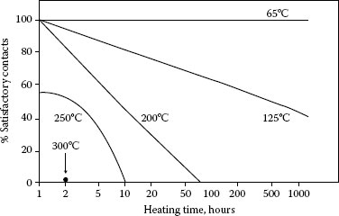
FIGURE 8.4
Effect of heating on contact reliability of 0.5 μm thick pure gold plating on a polished copper substrate [45]; probed at 1 N; criterion of satisfactory contact: Contact resistance not in excess of 1 mΩ.
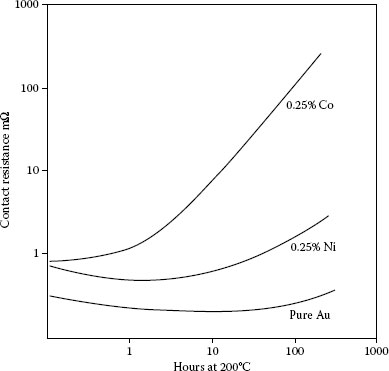
FIGURE 8.5
Thermal stability of contact resistance at 1 N of 50 μm thick gold plate; aged at 200°C; effect of cobalt and nickel additions (0.25%).
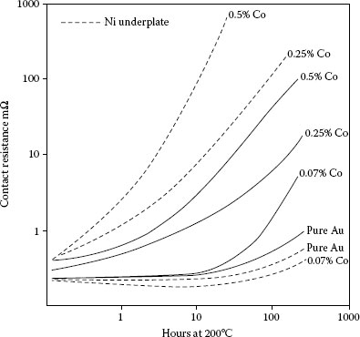
FIGURE 8.6
Thermal stability of contact resistance at 1 N of 2.5 μm hard gold plates containing 0.07, 0.25, or 0.5% cobalt without (solid, lines) and with (dashed lines) 2.5 μm nickel underplate; copper substrate, aged at 200°C.
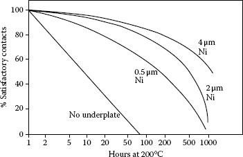
FIGURE 8.7
Effect of heating at 200°C on the contact reliability of 0.5 μm thick pure gold plate on a polished copper substrate without and with various thicknesses (0.5, 2, 4 μm) of nickel underplate. Probed at 1 N. Criterion of satisfactory contact: contact resistance not in excess of 1 mΩ.
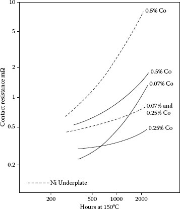
FIGURE 8.8
Thermal stability of contact resistance at 1 N of thin (0.5 μm) hard gold plates on copper containing 0.07, 0.25, or 0.5% cobalt without (solid lines) and with (dashed lines) 2.5 μm nickel underplate. Aged at 150°C.
In the gold-plated copper system, hard golds degrade more quickly than pure gold and gold alloys with noble metals such as palladium (Figure 8.5). This is due to the diffusion of the base metal hardener and polymer constituents to the surface of the hard gold [43]. Golds hardened with nickel show more stable contact resistance on thermal aging those hardened with cobalt as shown in Figure 8.5 [43,46]. There is an expected dependence of rate of change of contact resistance to the content of the base metal in the gold at a given thickness (Figure 8.6) [43].
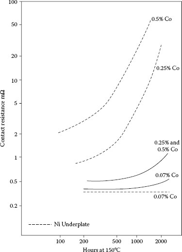
FIGURE 8.9
Same as Figure 8.8, except with thick (2.5 μm) cobalt–hard gold plates.
Nickel underplate has long been recognized to be a diffusion barrier for copper, zinc, and other metals used as underplates and for effectively retarding the rate of change of contact resistance of pure gold (see Figure 8.7; [45]). But it may have the opposite effect when the finish is hard gold, depending on the hardener used ([43]; Figures 8.6, 8.8, and 8.9). This may be because the composite hardness of the finish, consisting of gold and nickel underplate, is greater, which lowers the deformability under load of the finish. Nickel underplate is harder than hard golds containing significant (tenths of a percent) of cobalt or nickel. The films originate in base metals in the hard golds rather than as diffused species from the substrate as with pure gold without an underplate. With reduced deformability, insulating films are less readily displaced. An alternative hypothesis is without the barrier layer, the hardener species can diffuse both ways, to the external surface and into the substrate. The latter would reduce the concentration of the oxidizable species on the external surface, and thus, retard the growth kinetics of the resistive film. In the presence of the nickel barrier, the diffusion is only towards the external surface. Therefore, the amount of diffused metal at the gold surface (in the form of an insulating film) would be greater with the nickel underplate, consequently with a more pronounced degrading effect on contact resistance. This apparent adverse effect of nickel underplate for hard golds is surprising, for its role as a diffusion barrier has been considered to be a reason for its use.
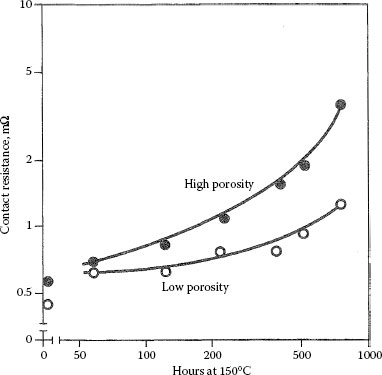
FIGURE 8.10
Contact resistance of pure gold platings, 0.15 μm thick, on copper: O low porosity gold; ● high porosity gold. Aged at 150°C. Probed at 0.25 N. The low porosity deposit had about 25–80 plating had > 1000 pores cm−2. (See Ref. [48] for details.)
Thin, pure gold degrades more rapidly than thick deposits [43] because the diffusion path for the underplate and substrate metals is shorter. The reverse is true for hard golds, perhaps because thick deposits have more total base metal. This effect is especially pronounced with hard golds on a nickel underplate, as can be seen in Figures 8.8 and 8.9.
It has also been found that the environment plays a role in changes in contact resistance. If oxidation of diffused base metal at the surface is the rate-limiting step rather than diffusion, then reactions other than oxidation may increase the rate of change of contact resistance. It has been found that chlorine in the atmosphere can cause more rapid increases of contact resistance than clean air [47]. Printed circuit boards with fire retardants are a source of chlorine. The dependence of rate of change of contact resistance on grain size is predictable, as is porosity of the deposit (Figure 8.10), for grain boundaries and pores are the diffusion paths for the defects [48]. Figure 8.11 (not probed according to ASTM B667) plots the times to obtain given increases in contact resistance for a hard gold on phosphor bronze as a function of temperature with an Arrhenius extrapolation to longer times [49].
Table 8.6 is a short list of maximum temperatures to which finishes in their usual thicknesses on nickel underplate can be heated, based on the author’s experience. Silver does not oxidize, and therefore is a preferred material, notwithstanding its tendency to tarnish if unprotected.
Pure palladium does not oxidize below 350°C and, being free of intrinsic polymers, has a considerably higher limit of thermal stability than hard golds. Palladium is also a diffusion barrier for copper and other metals. DG R-156 and 60Pd40Ag similarly have a higher temperature limit than hard golds. On the other hand, 80Pd20Ni is relatively poor due to its large nickel content, although a flash of pure or a hard gold can retard this degradation.
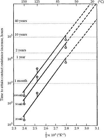
FIGURE 8.11
Time to attain contact resistance increases of 20, 50, and 100 mΩ for 0.3 μm cobalt-hard gold plated on phosphor bronze [49]. Probed at 0.1 N.
TABLE 8.6
For High-Reliability Applications, Maximum Temperatures at Which Coatings Can Be Heated for Extended Periodsa
Material |
Approximate Temperature (°C) |
0.38 μm plated pure Au on plated or solid Ni or Ni alloy spring materials; heat treated [12] |
>200 |
Ag |
>200 |
Pd, 60Pd40Ag, Rh (with and without Au flash) |
200 |
DG R-156 |
150 |
Hard golds |
125b |
80Pd20Ni |
<100c |
Au–Cu–Cd alloy electrodeposits |
<100 |
Sn, Sn–Pb alloys |
<100d |
a Recommended maximum temperatures are highly dependent on contact design, normal load, environment, coating, underplate and liner thicknesses, underplate-substrate composition and mechanical properties, and contact surface roughness.
b Temperature limit may be higher depending on hardener metal, its amount, gold thickness, and other factors (see Table 8.5).
a Increase to 125°C when gold flash is used.
a Higher temperatures may be satisfactory for non-critical applications.
AuCuCd platings (cyanide chemistry) are typical of many alloy golds that contain considerable base metal, and have relatively poor thermal stability [45]. Bright tin platings contain co-deposited organics which degrade their thermal stability, and matte (pure) tin has been found to be better. After extended aging, the tin can be entirely consumed in forming intermetallics with the copper or nickel on which it is coated. This is discussed in Section 8.4.2
The development of coatings having stable contact resistance at high temperatures has been stimulated by the proliferation of connectors for automotive underhood applications. Recent reports on some of these coatings discuss: clad thin layers of 69Au25Ag6Pt on 60Pd40Ag with a nickel liner [50], vapor-deposited thin gold or 80Pd20Ni on vapor-deposited nickel [51] and gold flash on a multilayered palladium-based finish [52].
The effect of growth of intermetallic compounds on the contact properties of electronic connectors with tin finishes has been determined. Extensive studies have also been made with tin and other metals for utility connectors (Chapters 1 and 5). These studies were prompted by the realization that intermetallic compounds can form rapidly, even at low temperatures and especially at elevated temperatures [53]. Contact finishes are thin and the electrical and mechanical properties of intermetallics are very different from those of the parent metals. Intermetallics are less conductive (by a factor ~ 10) and harder (by a factor ~ 5),and these changes can degrade contact resistance [54].
Figure 8.12 shows the growth of intermetallics on copper for some tin and tin–lead alloy coatings at 24°C and 50°C [55,56]. The rate of growth on nickel is slightly lesser [57,56]. The intermetallics from tin and copper are Cu6Sn5 (for temperatures <150C) [53] and Cu3Sn and Cu6Sn5 (for temperatures >150°C) [53] and for tin and nickel Ni3Sn4 (with possibly other compounds) [57,58]. The demarcations between the intermetallic layers are highly irregular.
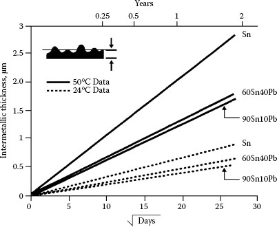
FIGURE 8.12
Growth of intermetallic compound layers at interface for tin and tin–lead alloys at 24 and 50°C [55]. Inset shows typical convoluted thickness of the layers.
The contact resistance of tin on various substrates with copper and nickel underplatings after seven years of exposure at 50°C, followed by one year at 20°C, is plotted in Figure 8.13 [59]. Contact resistance was determined by probing. In general, it increased significantly, although the data are scattered. A sulfur dioxide exposure after aging attenuated the increase in contact resistance. Fine-grained, bright tin was poorer than matte tin. The contact resistance of tin–lead alloy after similar aging was much better behaved.
The conclusion from these experiments, coupled with other considerations, is that bright tin plating is an inferior metal for contact applications. Although matte tin is, it is not prudent to use it for high-reliability, long-duration applications. The susceptibility of these finishes to film formation in atmospheres polluted with chlorine and nitrogen dioxide is well known [60], and they are also prone to degradation by fretting corrosion. The solderability of tin coated contacts is degraded on aging, which limits the shelf life of contacts with these finishes.
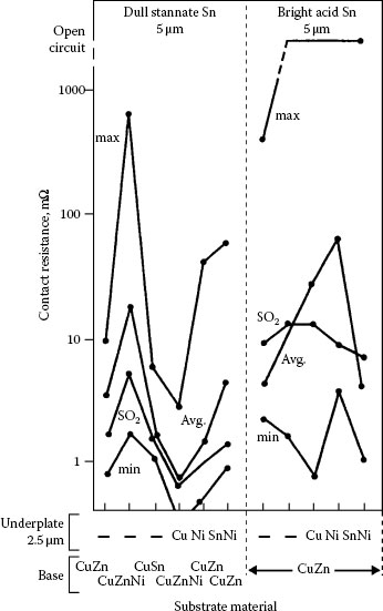
FIGURE 8.13
Contact resistance of dull and bright tin coatings aged at 50°C on various substrates and underplates [59]. Average, minimum, and maximum values are shown after 7 years in air and the average after an additional exposure to 0.15 p.p.m. SO2 at 70% RH, 25°C, for 35 days. Probed at 1 N.
Whiskers are filamentary growths that often develop spontaneously on the surface of pure tin, zinc, and cadmium [1,61,62,63,64,65]. They are single crystals which grow by diffusion at their base from the surface of the finish. Whiskers may be straight or convoluted, are of varied length, often to 1 cm, and typically are 1–5 μm in diameter. Their population density may be as high as 104 cm−2 of surface. Figure 8.14 [64] illustrates typical whiskers from a tin plating on copper. Although a complete understanding of growth of tin whiskers is, at present, not available, stress in the deposit certainly promotes the process [66]. Whiskers grow more rapidly on substrates in compression [65]. Their formation may depend on the composition of the substrate and the underplate, and on environmental factors. Whisker density and length is greater on a smooth tin surface than on a rough one [67]. Their growth is enhanced in an ambient with very high humidity: 65%–90%RH.
Whiskers may be detrimental if they bridge adjacent contacts (Figure 8.15) [68]. They can carry currents to about 25 mA; higher currents cause them to fuse. Reflowed deposits do not develop whiskers. In earlier times, growth of tin whiskers could be avoided with finishes that contained 5% or lesser of lead. Thus, in the past it was considered to be poor practice to use pure tin platings on contacts, since tin–lead alloy deposits were a practical solution to the whisker problem. Now, however, lead is banned from almost all contact applications to eliminate problems of lead poisoning. So, there has been a change from tin–lead solders and the use of lead in tin plate. This has led to increased research into prevention and control of formation of tin whiskers [66].
The answer to the problem of uncontrolled automobile acceleration, that was seen a few years ago, was eventually traced to shorting of the Accelerator Pedal Position (APP) sensor due to tin whiskers [69]. This sensor controlled the vehicle’s acceleration, but when shorted by whiskers 11 μm diameter, it could no longer function to prevent the uncontrolled acceleration. Leidecker et al. [69] showed that to test for these very fine whiskers, one had to be careful to not apply too high a voltage. If such a high voltage is applied across these whiskers, they would be ruptured. The researchers said this was one reason that the whisker problem was not identified sooner.
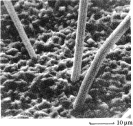
FIGURE 8.14
An array of closely spaced tin whiskers. Finish is 5 μm of tin on a copper substrate [64].
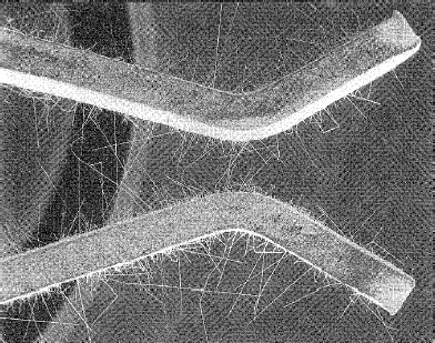
FIGURE 8.15
Whisker growth on tin-plated contacts. (From RP Diehl and NA Cifaldi, Proc 8th Ann Conn Sym, Cherry Hill, 327–36, 1975.)
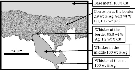
FIGURE 8.16
Diagram of a cross-section through a silver whisker from a silver plated copper substrate showing its composition [70].
Silver Sulfide (Ag2S) is a major corrosion product on silver-plated surfaces in an ambient with concentrations of a sulfuric gas such as H2S [1]. Once the Ag2S layer is in place, whiskers of silver can begin to form [1,70]. Unlike the tin whiskers that form from a surface of pure tin, the silver whiskers require a layer of Ag2S before they begin to form. Although the corrosion layer is necessary, Chudnovsky [70] has shown that the whisker is made up almost entirely of silver; see Figure 8.16. The metallic nature of this whisker means that it is highly conductive and can easily cause adjacent conductors to short and fail.
8.5 Physical and Mechanical Properties
8.5.1 Characteristics of Layered Systems
The hardness of a contact finish depends on the deformability of its individual layers and the substrate, their thicknesses, and the load. Hardness is an important characteristic of contacts because it is one of the controlling parameters of the size of an a-spot and constriction resistance. When base metal contact finishes are covered by insulating films such as oxides, the extent of the disruption of these films in connections also depends on hardness; the success of soft base coatings such as tin lies in the ease with which its superficial oxides can be penetrated. In addition, the durability of finishes that are subjected to sliding and fretting is in part controlled by hardness. Examples of these effects are illustrated in Chapter 6. A method for calculating the hardness of layered systems has been proposed [71]. Examples of composite hardnesses are given in Tables 8.7 and 8.8.
The contact resistance of finishes depends on the hardness, thickness, and conductivity of the constituent layers, as well as on the load. This is discussed in Chapter 1. In the case of base metal contacts, whether plated or solid, that are covered with insulating films, the geometry and dimensions of the opposing contact are also the determining factors. So-called, “sharp” contacts are better able to penetrate these films. Probe contacts made of hard metals resist deformation better than those that are soft, and therefore exert higher pressure. This is illustrated in Figure 8.17, a determination of the contact resistance of oxide-covered 65Sn35Ni electrodeposit, copper, and nickel [72]. Hard, sharp contacts, generally plated with hard golds, are used in commercial probe testers for determining the functioning of integrated circuits in production control. The slopes of the curves showing contact resistance versus force characteristics for plated contacts illustrate the relative contributions of the finish and the substrate (Figure 8.18) [73].
TABLE 8.7
Hardness of Plated Contact Materialsa
Cobalt–gold (μm) |
Nickel Underplate (μm) |
Substrate (thickness, mm) |
Depth of Penetration of Identer (μm)b |
×102 Nmm−2 Knoop, 0.25 N |
2 |
none |
Cu (3.2) |
2.6 |
5.6 |
2 |
2.5 |
Cu (3.2) |
2.5 |
6.3 |
3.3 |
2.5 |
Cu (3.2) |
2.0 |
9.3 |
3.3 |
4 |
Cu (3.2) |
1.7 |
13.1 |
2 |
2.5 |
Be-Cu (4.9) |
1.1 |
28.8 |
a Hardness determined normal to surface.
Hardness of bulk materials from metallographic sections (×102 Nmm−2°) |
||
Co-gold |
18 |
(Knoop, 0.25 N) |
Ni underplate |
55 |
(Knoop, 0.1 N) |
Substrate, Cu |
4–6 |
(Knoop, 0.25 N) |
Substrate, Be–Cu |
26.6 |
(Knoop, 0.25 N) |
TABLE 8.8
Hardness of Plated Contact Materials
Soft Gold (μm) |
70Pd30Ni (μm) |
Ni Underplate (μm) |
Substrate (μm) |
×102 Nmm−2 Vickers, 1N |
0.15–0.40 |
2.5 |
– |
22.5 |
12.9 |
0.15–0.40 |
2.5 |
1.2 |
22.5 |
15.2 |
Hardness of bulk materials from metallographic sections |
||
Soft gold |
85 |
kg mm−2 (Vickers, 1 N) |
70Pd30Ni |
400 |
kg mm−2 (Vickers, 1 N) |
Ni underplate |
230 |
kg mm−2 (Vickers, 1 N) |
Substrate, Cu |
125 |
kg mm−2 (Vickers, 1 N) |
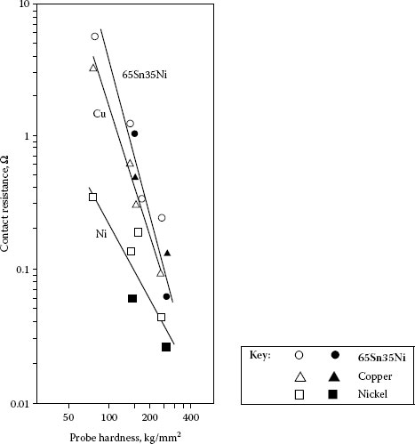
FIGURE 8.17
Median values of contact resistance at 0.5 N for aged 65Sn35Ni electrodeposit, solid copper, and solid nickel determined with various probe metals (hemispherically ended, 3.2 mm diameter [72]. Open symbols are for noble metal probes and solid symbols for copper and nickel probes.
The topography of most electrodeposited contact finishes is generally similar to that of the surfaces on which they are plated. However, some processes have a leveling effect in that deposition occurs preferentially in the valleys of the substrate surface, while other processes plate preferentially on the high spots. This is illustrated in Figure 8.19. Copper leveling underplates are used to obtain smooth surfaces for top plates made of precious metal. The thickness of the deposit must be of the order of the surface roughness to obtain any noticeable improvement. Leveling nickel is unsuitable as an underplate because it is brittle, which makes it impractical to form a contact after plating. These micro-throwing characteristics should be distinguished from macro-throwing properties which refer to the ability of a process to plate into recesses such as connector sockets. Another topographic feature of some deposits is nodularity. Figure 8.20 illustrates a nodular finish. Nodules can develop due to co-deposited particulates from poorly filtered plating solutions and from other causes. When a nodular deposit is due to its nickel underplate, the result is a finish which can abrade a softer opposing surface during engagement. The composite hardness of finishes with a nickel underplate is greater than that of common top plates, such as hard golds, as shown in Table 8.7.
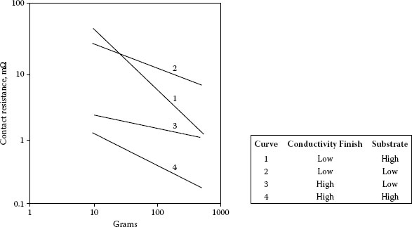
FIGURE 8.18
Contact resistance-force characteristics for some plated contact materials. (Schematic adapted from HN Wagar, In Physical Design of Electronic Systems, Vol. III, [eds. D Baker, D Koehler, W Fleckenstein, C Roden, R Sabia] Upper Saddle River, NJ: Prentice-Hall, 439–99, 1971 [73].)
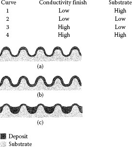
FIGURE 8.19
Schematic illustrations of various microthrowing characteristics of electrodeposits: (a) negative throw; (b) geometric throw; (c) leveling throw.
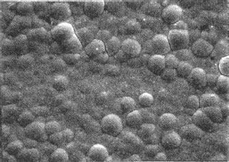
FIGURE 8.20
Nodular finish. Gold-flashed palladium on a nickel underplate. 1000 times magnified.
I (PGS) am very grateful to Marjorie Myers who critically reviewed this chapter and who suggested additions that have helped make the contents a more thorough review of coating and plating technology.
1. W Schmitt, S Franz, J Heber, O Lutz, and V Behrens, Formation of silver sulfide layers and their influence on the electrical characteristics of contacts in the field of information technology, Proc 24th Int Conf Elect Cont, 489–94, 1982.
2. FE Bader, Diffused gold R156: A new inlay contact material for bell system connectors, Proc 11th Int Conf Elect Cont, 133–37, 1982.
3. N. Aukland, H. Hardee, A. Wehr-Aukland, and P. Lees, A comparison of a clad material (65Au21Pd14Ag) and an electroplated gold over palladium material system under fretting conditions at elevated temperatures, Proc 45th IEEE Holm Conf Elect Cont, 213–25, 1999.
4. M. Myers, Comparison of hard Au versus hard Au-flashed PdNi as a Contact finish, Proc 56th IEEE Holm Conf Elect Cont, 49–57, 2010.
5. JA Abys, HK Straschil, I Kadija, EJ Kudrak, and J Blee, The electrodeposition and material properties of palladium–nickel alloys, Metal Finish 89 (7), 43–52, 1991.
6. W Zhang, M Clauss, J Guebey, and F Schwager, Low ammonia, high-speed palladium–nickel electroplating process for connector applications, Metal Finish 65 (1), 33–37, March 2009.
7. M Myers, The performance implications of silver as a contact finish in traditionally gold finished contact applications, Proc 55th IEEE Holm Conf Elect Cont, 307–15, 2009.
8. There are a number of inhibitor materials that claim to protect Ag from tarnishing, Here is a very non-complete list of examples: Evabrite, Tarnaban, Silverbrite W TPS, Antitarnish 616.
9. S. Yang, J Wu, and M Pecht, Electrochemical migration of land grid array sockets under highly accelerated stress conditions, Proc 51st IEEE Holm Conf Elect Cont, 238–45, 2005.
10. C Dervos, J Novakovic, and P Vassiliou, Electroless Ni–B and Ni–P coatings with high-fretting resistance for electrical contact applications, Proc 51st IEEE Holm Conf on Elect Cont, 281–88, 2005.
11. B Chudovsky, Degradation of power contacts in industrial atmosphere: Plating alternative to Ag and Sn, Proc 49th IEEE Holm Conf Elect Cont, 98–4, 2003.
12. Y Okinaka, et al., Polymer inclusions in cobalt-hardened electroplated gold, J Electrochem Soc 125 (11): 1745–750, 1978.
13. Okinaka and S Nakahara, Structure of electroplated hard gold observed by transmission electron microscopy, J Electrochem Soc 123 (9): 1284–1289, 1976.
14. M Antler, Structure of polymer co-deposited in gold electrodeposits, Plating 60 (5): 468–74, 1973.
15. Electrodeposition of hard golds: A hypothesis to explain its special features, Gold Bulletin 11 (4): 132–33, 1978 (according to research by E.T. Eisenmann).
16. FI Nobel, et al., An evaluation of 18 karat and 24 karat hard gold deposits for contact applications, Proc 4th Plat Electro Ind Sym, American Electroplaters’ Society, Indianapolis, 106–30, 1973.
17. FB Koch, et al., Additive-free hard gold plating for electronics applications (in two parts), Plat Surf Fin 67 (6): 50–54, 1980; 67 (7): 43–45, 1980.
18. BDT plating processes, Sel-Rex Corporation, Nutley, NJ.
19. RG Baker, and TA Palumbo, The potential role of ruthenium for electronic applications, Plat Surf Fin 69 (11): 61–68, 1982.
20. I Boguslavasky, et al., Electroplating of PdCo alloy for connector applications, Proc Int Inst Conn Interconn Tech Conf, 217–36, 1996.
21. M Naillat, et al., Tribological behavior of Pd–Ni–Co electrodeposited alloys, Proc 13th Int Conf Elect Cont, 468–75, 1986.
22. JAE Bell and D Hope, Corrosion resistant high temperature contacts, Proc Conn Interconn Tech Sym International Institute of Connector and Interconnection Technology Inc., San Jose, 345–52, 1992.
23. F Houze, et al., Electrical characterization of thin polyacrylonitrile electropolymerized on nickel for connector applications, Proc 16th Int Conf Elect Cont, 267–71, 1992.
24. G Herklotz, et al., Application of sputtered layers in contact technology, Proc 15th Int Conf Elect Cont, 182–92, 1990.
25. M Antler and SJ Krumbein, Contact properties of conductive hardmetals and tin nickel plate, Proc 11th Eng Sem Elect Cont, 103–38, 1965.
26. S Benhenda, TiN coating in electrical contacts applications, Proc 16th Int Conf Elect Cont, 181–84, 1992.
27. PW Leech, The effect of nitrogen implantation in the tribological properties of gold-based alloys and electroplated palladium, Proc 33rd IEEE Holm Conf Elect Cont, 53–62, 1987.
28. M Sun, et al., Modification of Ag-plated contacts by nitrogen ion implantation, Proc 18th Int Conf Elect Cont, Chicago, 467–71, 1996.
29. M. Antler, et al., The effect of boron implantation on the sliding wear and contact resistance of palladium, 60Pd40Ag, and a CuNiSn Alloy, IEEE Trans Comp Hyb Manuf Tech CHMT–5 (1): 81–84, 1982.
30. H. Anli, Investigation on improving wear resistance of electric contact materials for aviation by ion implantation, Proc 16th Int Conf Elect Cont, 235–39, 1992.
31. An example can be found at www.impactcoatings.se
32. CA Haque, Characterization of metal-in-elastomer connector contact material, Proc 35th IEEE Holm Conf Elect Cont, Chicago, 117–22, 1989.
33. G Rosen, et al., A comparison of metal-in-elastomer connectors: The influence of structure on mechanical and electrical performance, Proc 15th Int Conf Elect Cont, 151–65, 1990.
34. M Clarke, Porosity and porosity tests, In Properties of Electrodeposits, Their Measurement and Significance, (eds) R. Sard, H. Leidheiser Jr, and F. Ogburn, Princeton: The Electrochemical Society, 122–141, 1975.
35. SM. Garte, Porosity, In Gold Plating Technology, (eds) F.H. Reid and W. Goldie, Ayr: Electrochemical Publications, Ltd, 295–315 and 345–59, 1974.
36. A Sun, H Moffat, D Enos, and C Glauner, Pore corrosion model for gold-plated copper contacts, Proc 51st IEEE Holm Conf Elect Cont, 232–37, 2005.
37. SM. Garte, Effect of substrate roughness on the porosity of gold electrodeposits, Plating 53: 1335–40, 1966.
38. M Antler, Gold-plated contacts: Effect of substrate roughness on reliability, Plating 56: 1139–1144, 69.
39. YL Zhou, XY Lin, and JG Zhang, The electrical and mechanical performance of corroded products on gold plating after long-term indoor air exposure, Proc 46th IEEE Holm Conf Elect Cont, 18–26, 2000.
40. M Antler, et al., The corrosion resistance of worn tin–nickel and gold coated tin–nickel alloy electrodeposits, J Electrochem Soc 124 (17): 1069–1075, 1997.
41. M Antler, Corrosion control with tin nickel and other intermetallics. In Corrosion Control by Coatings, (ed.) H. Leidheiser Jr, Princeton: Science Press, 115–33, 1979.
42. UB. Thomas (Bell Labs). Unpublished work.
43. M Antler, Gold-plated contacts: Effect of thermal aging on contact resistance, Proc 43rd IEEE Holm ConfElect Cont, Philadelphia, 121–31, 1997.
44. M Pinnel, et al., Oxidation of copper from gold alloy solution at 50°C–150°C, J Electrochem Soc 126 (10): 1798–805, 1979.
45. M Antler, Gold-plated contacts: Effect of heating on reliability, Plating 57: 625–28, 1970.
46. M Huck, Kontakteigenschaften galvanischer hartgoldschichten bei erhöhten temperaturen, Metallwissenschaft und Technik 46(1): 32–35, 1992.
47. HG Tompkins and MR Pinnel, Low-temperature diffusion of copper through gold, J Appl Phy 47(9): 380–12, 1976.
48. M Antler and MH Drozdowicz, Gold-plated contacts: The relationship between porosity and contact resistance on elevated temperature aging, Plat Surf Fin 63 (9): 19–21, 1976.
49. L Revay, Surface accumulation rate of diffusing species on thin gold electroplates, IEEE Trans Comp, Hyb Manuf Tech CHMT–15(5): 870–75, 1992.
50. PW Lees, Connector contact finishes for high temperature automotive applications, Proc Int Inst Conn Interconn Tech Conf, Boston, 241–50, 1996.
51. YT Cheng, et al., Vapor-deposited thin gold coatings for high-temperature electrical contacts, Proc 42nd IEEE Holm Conf Elect Cont, 404–13, 1996.
52. E Kudrak, et al., A high-temperature electrical contact finish for automotive app lications, Proc SUR/FIN 1996, American Electroplaters and Surface Finishers Society, 1996.
53. WM Wang, AQ He, Q Liu, and DG Ivey, Solid state interfacial reactions in electrodeposited Cu–Sn couples, Trans Non-ferr Met Soc China, 20: 90–96, 2010.
54. M Braunovic, Effect of intermetallic phases on the performance of tin-plated copper connections and conductors, Proc 49th IEEE Holm Conf Elect Cont, 124–31, 2003.
55. D.A. Unsworth and C.A. Mackay, A preliminary report on growth of compound layers on various metal bases plated with tin and its alloys, Trans Inst Met Fin 51: 85–90, 1973.
56. PA Kay and CA Mackay, The growth of intermetallic compounds on common basis materials with tin and tin-lead alloys, Trans Inst Met Fin 54: 68–74, 1976.
57. S. Noël, N. Lécaudé, S. Correia, P. Gendre, and A. Grosjean, Electrical and tribological properties of tin-plated copper alloy for electrical contacts in relation to intermetallic growth, Proc 51st IEEE Holm Conf Elect Cont, 1–10, 2006.
58. S. Noel, D Alamarguy, S Correia, and P. Gendre, Study of thin underlayers to hinder contact resistance increase due to intermetallic compound formation, Proc 55th IEEE Holm Conf Elect Cont, 153–159, 2009.
59. U Lindborg, et al., Intermetallic growth and contact resistance on tin contacts after Aging, Proc 21st Holm Sem Elect Cont, 25–31, 1975.
60. M Antler, et al., Base metal contacts: an exploratory study of separable connection to tin–lead, IEEE Trans Parts, Hyb Packag PHP–11: 35–44, 1975.
61. KJ Compton, et al., Filamentary growth on metal surfaces: Whiskers, Corrosion 7: 327–34, 1951.
62. RM Fisher, et al., Accelerated growth of tin whiskers, Acta Met 2: 368–73, 1954.
63. GT Galyon, Annotated tin whisker bibliography and anthology, IEEE Trans Electron Packag Manuf 28: 94, 2005.
64. PL Key, Surface morphology of whisker crystals of tin, zinc and cadmium, Proc IEEE Electron Comp Conf, 155–60, 1970.
65. E Crandall, G Flowers, R Jackson, P Lall and M Bozack, Growth of Sn whiskers under net compressive and tensile stress states, Proc 57th IEEE Holm Conf Elect Cont, 304–308, 2011.
66. G Gaylon, Whisker formation concepts: The end game, IEEE Trans Comp, Packag Tech 1 (3): 1098–109, 2011.
67. C Rodekohr, G Flowers, J Suhling, and M Bozack, Influence of substrate surface roughness on tin whisker growth, Proc 54th IEEE Holm Conf Elect Cont, 245–48, 2008.
68. RP Diehl and NA Cifaldi, Elimination of tin whisker growth on interconnections, Proc 8th Ann Conn Sym, Cherry Hill, 327–36, 1975.
69. H Leidecker, L Panashchenko, and J Brusse, Electrical failure of an accelerator pedal position sensor caused by tin whisker and discussion of investigative techniques used for whisker detection, 5th Int Tin Whisk Sym, 2011. http://nenasa.gov/whisker
70. B Chudnovsky, Degradation of power contacts in industrial atmosphere: silver corrosion and whiskers, Proc 48th IEEE Holm Conf Elect Cont, 140–50, 2002.
71. PA Engel, Vickers microhardness evaluation of multilayer platings for electrical contacts, Proc IEEE Holm Conf Elect Cont, Chicago, 66–72, 1991.
72. M Antler, Contact resistance of oxidized metals: dependence on the mating material, IEEE Trans Comp, Hyb Manuf Tech CHMT–10 (3): 420–424, 1987.
73. HN Wagar, Principles of conduction through electrical contacts, In Physical Design of Electronic Systems, (eds) D. Baker, D. Koehler, W. Fleckenstein, C. Roden, and R. Sabia, Vol. III, Upper Saddle River, NJ: Prentice-Hall, 439–99, 1971.