
Chapter 12. Signal Processing and Conditioning
Typically a sensor cannot be directly connected to the instruments that record, monitor, or process its signal, because the signal may be incompatible or may be too weak and/or noisy. The signal must be conditioned—that is, cleaned up, amplified, and put into a compatible format.
The following sections discuss the important aspects of sensor signal conditioning.
12.1. Conditioning Bridge Circuits
12.1.1. Introduction
This section discusses the fundamental concepts of bridge circuits.
Resistive elements are some of the most common sensors. They are inexpensive to manufacture and relatively easy to interface with signal conditioning circuits. Resistive elements can be made sensitive to temperature, strain (by pressure or by flex), and light. Using these basic elements, many complex physical phenomena can be measured, such as fluid or mass flow (by sensing the temperature difference between two calibrated resistances) and dew-point humidity (by measuring two different temperature points). Bridge circuits are often incorporated into force, pressure, and acceleration sensors.
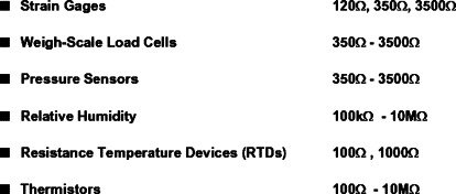
Sensor elements' resistances can range from less than 100Ω to several hundred kiloohms, depending on the sensor design and the physical environment to be measured (see Figure 12.1). For example, RTDs (resistance temperature devices) are typically 100Ω or 1000Ω. Thermistors are typically 3500Ω or higher.
Figure 12.1. Resistance of popular sensors.
12.1.2. Bridge Circuits
Resistive sensors such as RTDs and strain gauges produce small percentage changes in resistance in response to a change in a physical variable such as temperature or force. Platinum RTDs have a temperature coefficient of about 0.385%/° C. Thus, in order to accurately resolve temperature to 1° C, the measurement accuracy must be much better than 0.385Ω, for a 100-Ω RTD.
Strain gauges present a significant measurement challenge because the typical change in resistance over the entire operating range of a strain gauge may be less than 1% of the nominal resistance value. Accurately measuring small resistance changes is therefore critical when applying resistive sensors.
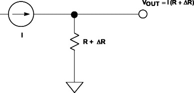
One technique for measuring resistance (shown in Figure 12.2) is to force a constant current through the resistive sensor and measure the voltage output. This requires both an accurate current source and an accurate means of measuring the voltage. Any change in the current will be interpreted as a resistance change. In addition, the power dissipation in the resistive sensor must be small, in accordance with the manufacturer's recommendations, so that self-heating does not produce errors, therefore the drive current must be small.
Figure 12.2. Measuring resistance indirectly using a constant current source.
Bridges offer an attractive alternative for measuring small resistance changes accurately. The basic Wheatstone bridge (actually developed by S. H. Christie in 1833) is shown in Figure 12.3. It consists of four resistors connected to form a quadrilateral, a source of excitation (voltage or current) connected across one of the diagonals, and a voltage detector connected across the other diagonal. The detector measures the difference between the outputs of two voltage dividers connected across the excitation.
Figure 12.3. The Wheatstone bridge.
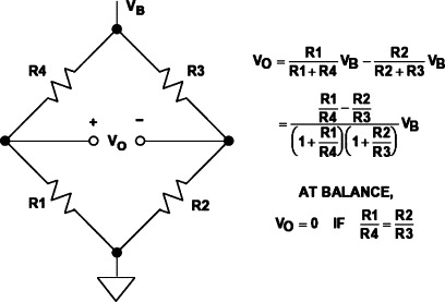
A bridge measures resistance indirectly by comparison with a similar resistance. The two principal ways of operating a bridge are as a null detector or as a device that reads a difference directly as voltage.
When R1/R4 = R2/R3, the resistance bridge is at a null, regardless of the mode of excitation (current or voltage, AC or DC), the magnitude of excitation, the mode of readout (current or voltage), or the impedance of the detector. Therefore, if the ratio of R2/R3 is fixed at K, a null is achieved when R1 = K · R4. If R1 is unknown and R4 is an accurately determined variable resistance, the magnitude of R1 can be found by adjusting R4 until null is achieved. Conversely, in sensor-type measurements, R4 may be a fixed reference, and a null occurs when the magnitude of the external variable (strain, temperature, etc.) is such that R1 = K · R4.
Null measurements are principally used in feedback systems involving electromechanical and/or human elements. Such systems seek to force the active element (strain gauge, RTD, thermistor, etc.) to balance the bridge by influencing the parameter being measured.
For the majority of sensor applications employing bridges, however, the deviation of one or more resistors in a bridge from an initial value is measured as an indication of the magnitude (or a change) in the measured variable. In this case, the output voltage change is an indication of the resistance change. Because very small resistance changes are common, the output voltage change may be as small as tens of millivolts, even with VB = 10V (a typical excitation voltage for a load cell application).
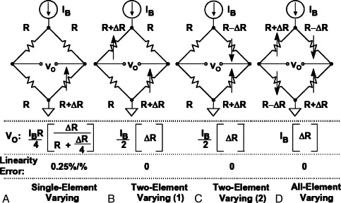
In many bridge applications, there may be two, or even four, elements that vary. Figure 12.4 shows the four commonly used bridges suitable for sensor applications and the corresponding equations which relate the bridge output voltage to the excitation voltage and the bridge resistance values. In this case, we assume a constant voltage drive, VB. Note that, since the bridge output is directly proportional to VB, the measurement accuracy can be no better than that of the accuracy of the excitation voltage.
Figure 12.4. Output voltage and linearity error for constant voltage drive bridge configurations.

In each case, the value of the fixed bridge resistor, R, is chosen to be equal to the nominal value of the variable resistor(s). The deviation of the variable resistor(s) about the nominal value is proportional to the quantity being measured, such as strain (in the case of a strain gauge) or temperature (in the case of an RTD).
The sensitivity of a bridge is the ratio of the maximum expected change in the output voltage to the excitation voltage. For instance, if VB = 10V and the full-scale bridge output is 10 mV, then the sensitivity is 1 mV/V.
The single-element varying bridge is most suited for temperature sensing using RTDs or thermistors. This configuration is also used with a single resistive strain gauge. All the resistances are nominally equal, but one of them (the sensor) is variable by an amount ΔR. As the equation indicates, the relationship between the bridge output and ΔR is not linear. For example, if R = 100Ω and ΔR = 0.152 (0.1% change in resistance), the output of the bridge is 2.49875 mV for VB = 10V. The error is 2.50000 mV – 2.49875 mV, or 0.00125 mV. Converting this to a percent of full scale by dividing by 2.5 mV yields an end-point linearity error in percent of approximately 0.05%. (Bridge end-point linearity error is calculated as the worst error in percent of full scale from a straight line that connects the origin and the end point at full scale; that is, the full-scale gain error is not included). If ΔR = 1Ω (1% change in resistance), the output of the bridge is 24.8756 mV, representing an end-point linearity error of approximately 0.5%. The end-point linearity error of the single-element bridge can be expressed in equation form:

It should be noted that this nonlinearity refers to the nonlinearity of the bridge itself and not the sensor. In practice, most sensors exhibit a certain amount of their own nonlinearity which must be accounted for in the final measurement.
In some applications, the bridge nonlinearity may be acceptable, but there are various methods available to linearize bridges. Since there is a fixed relationship between the bridge resistance change and its output (shown in the equations), software can be used to remove the linearity error in digital systems. Circuit techniques can also be used to linearize the bridge output directly, and these will be discussed shortly.
There are two possibilities to consider in the case of the two-element varying bridge. In the first, Case 1, both elements change in the same direction, such as two identical strain gauges mounted adjacent to each other with their axes in parallel.
The nonlinearity is the same as that of the single-element varying bridge, however the gain is twice that of the single-element varying bridge. The two-element varying bridge is commonly found in pressure sensors and flowmeter systems.
A second configuration of the two-element varying bridge, Case 2, requires two identical elements that vary in opposite directions. This could correspond to two identical strain gauges: one mounted on top of a flexing surface, and one on the bottom. Note that this configuration is linear and, like two-element Case 1, has twice the gain of the single-element configuration. Another way to view this configuration is to consider the terms R + ΔR and R – ΔR as comprising the two sections of a center tapped potentiometer.
The all-element varying bridge produces the most signal for a given resistance change and is inherently linear. It is an industry-standard configuration for load cells that are constructed from four identical strain gauges.
Bridges may also be driven from constant current sources as shown in Figure 12.5. Current drive, although not as popular as voltage drive, has an advantage when the bridge is located remotely from the source of excitation because the wiring resistance does not introduce errors in the measurement. Note also that, with constant current excitation, all configurations are linear with the exception of the single-element varying case.
Figure 12.5. Output voltage and linearity error for constant-current drive bridge configurations.
In summary, there are many design issues relating to bridge circuits (Figure 12.6). After selecting the basic configuration, the excitation method must be determined. The value of the excitation voltage or current must first be determined. Recall that the full-scale bridge output is directly proportional to the excitation voltage (or current). Typical bridge sensitivities are 1 mV/V to 10 mV/V. Although large excitation voltages yield proportionally larger full-scale output voltages, they also result in higher power dissipation and the possibility of sensor resistor self-heating errors. On the other hand, low values of excitation voltage require more gain in the conditioning circuits and increase the sensitivity to noise.
Figure 12.6. Bridge considerations.
Regardless of its value, the stability of the excitation voltage or current directly affects the overall accuracy of the bridge output. Stable references and/or ratiometric techniques are required to maintain desired accuracy.
12.1.3. Amplifying and Linearizing Bridge Outputs
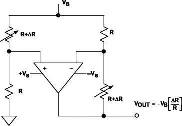
The output of a single-element varying bridge may be amplified by a single precision op-amp connected in the inverting mode as shown in Figure 12.7.
Figure 12.7. Using a single op-amp as a bridge amplifier for a single-element varying bridge.

This circuit, although simple, has poor gain accuracy and also unbalances the bridge due to loading from RF and the op-amp bias current. The RF resistors must be carefully chosen and matched to maximize the common mode rejection (CMR). Also it is difficult to maximize the CMR while at the same time allowing different gain options. In addition, the output is nonlinear. The key redeeming feature of the circuit is that it is capable of single-supply operation and requires a single op-amp. Note that the RF resistor connected to the noninverting input is returned to VS/2 (rather than ground) so that both positive and negative values of ΔR can be accommodated, and the op-amp output is referenced to VS/2.
A much better approach is to use an instrumentation amplifier (in-amp) as shown in Figure 12.8. This efficient circuit provides better gain accuracy (usually set with a single resistor, RG) and does not unbalance the bridge. Excellent common mode rejection can be achieved with modern in-amps. Due to the bridge's intrinsic characteristics, the output is nonlinear, but this can be corrected in the software (assuming that the in-amp output is digitized using an analog-to-digital converter and followed by a microcontroller or microprocessor).
Figure 12.8. Using an instrumentation amplifier with a single-element varying bridge.

Various techniques are available to linearize bridges, but it is important to distinguish between the linearity of the bridge equation and the linearity of the sensor response to the phenomenon being sensed. For example, if the active element is an RTD, the bridge used to implement the measurement might have perfectly adequate linearity; yet the output could still be nonlinear due to the RTD's nonlinearity. Manufacturers of sensors employing bridges address the nonlinearity issue in a variety of ways, including keeping the resistive swings in the bridge small, shaping complementary nonlinear response into the active elements of the bridge, using resistive trims for first-order corrections, and others.
Figure 12.9 shows a single-element varying active bridge in which an op-amp produces a forced null, by adding a voltage in series with the variable arm. That voltage is equal in magnitude and opposite in polarity to the incremental voltage across the varying element and is linear with ΔR. Since it is an op-amp output, it can be used as a low-impedance output point for the bridge measurement. This active bridge has a gain of 2 over the standard single-element varying bridge, and the output is linear, even for large values of ΔR. Because of the small output signal, this bridge must usually be followed by a second amplifier. The amplifier used in this circuit requires dual supplies because its output must go negative.
Figure 12.9. Linearizing a single-element varying bridge method 1.

Another circuit for linearizing a single-element varying bridge is shown in Figure 12.10. The bottom of the bridge is driven by an op-amp, which maintains a constant current in the varying resistance element. The output signal is taken from the right-hand leg of the bridge and amplified by a noninverting op-amp. The output is linear, but the circuit requires two op-amps which must operate on dual supplies. In addition, R1 and R2 must be matched for accurate gain.
Figure 12.10. Linearizing a single-element varying bridge method 2.

A circuit for linearizing a voltage-driven two-element varying bridge is shown in Figure 12.11. This circuit is similar to Figure 12.9 and has twice the sensitivity. A dual-supply op-amp is required. Additional gain may be necessary.
Figure 12.11. Linearizing a two-element varying bridge method 1 (constant-voltage drive).
The two-element varying bridge circuit in Figure 12.12 uses an op-amp, a sense resistor, and a voltage reference to maintain a constant current through the bridge.
![]()
Figure 12.12. Linearizing a two-element varying bridge method 2 (constant-voltage drive).
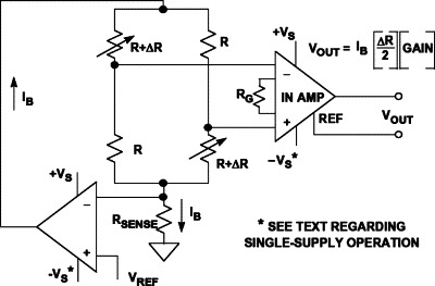
The current through each leg of the bridge remains constant (IB/2) as the resistances change; therefore the output is a linear function of ΔR. An instrumentation amplifier provides the additional gain. This circuit can be operated on a single supply with the proper choice of amplifiers and signal levels.
12.1.4. Driving Bridges
Wiring resistance and noise pickup are the biggest problems associated with remotely located bridges. Figure 12.13 shows a 350-Ω strain gauge that is connected to the rest of the bridge circuit by 100 ft of 30-gauge twisted-pair copper wire. The resistance of the wire at 25° C is 0.105Ω/ft, or 10.5Ω for 100 ft. The total lead resistance in series with the 350-Ω strain gauge is therefore 21Ω. The temperature coefficient of the copper wire is 0.385%/° C. Now we will calculate the gain and offset error in the bridge output due to a +10° C temperature rise in the cable. These calculations are easy to make, because the bridge output voltage is simply the difference between the output of two voltage dividers, each driven from a +10-V source.
Figure 12.13. Errors produced by wiring resistance for remote resistive bridge sensor.
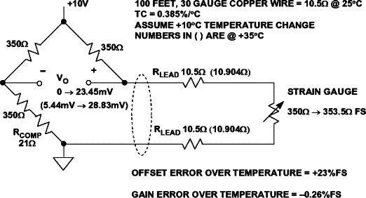
The full-scale variation of the strain gauge resistance (with flex) above its nominal 350-Ω value is +1% (+3.5Ω), corresponding to a full-scale strain gauge resistance of 353.5Ω, which causes a bridge output voltage of +23.45 mV. Notice that the addition of the 21-Ω RCOMP resistor compensates for the wiring resistance and balances the bridge when the strain gauge resistance is 350Ω. Without RCOMP, the bridge would have an output offset voltage of 145.63 mV for a nominal strain gauge resistance of 350Ω. This offset could be compensated for in software just as easily, but for this example, we chose to do it with RCOMP.
Assume that the cable temperature increases +10° C above nominal room temperature. This results in a total lead resistance increase of +0.404Ω (10.5Ω × 0.00385/° C × 10° C) in each lead. Note: The values in parentheses in the diagram indicate the values at +35° C. The total additional lead resistance (of the two leads) is +0.808Ω. With no strain, this additional lead resistance produces an offset of +5.44 mV in the bridge output. Full-scale strain produces a bridge output of +28.83 mV (a change of +23.39 mV from no strain). Thus the increase in temperature produces an offset voltage error of +5.44 mV (+23% full scale) and a gain error of −0.06 mV (23.39 mV – 23.45 mV), or −0.26% full scale. Note that these errors are produced solely by the 30-gauge wire and do not include any temperature coefficient errors in the strain gauge itself.
The effects of wiring resistance on the bridge output can be minimized by the three-wire connection shown in Figure 12.14. We assume that the bridge output voltage is measured by a high-impedance device, therefore there is no current in the sense lead. Note that the sense lead measures the voltage output of a divider: The top half is the bridge resistor plus the lead resistance, and the bottom half is strain gauge resistance plus the lead resistance. The nominal sense voltage is therefore independent of the lead resistance. When the strain gauge resistance increases to full scale (353.5Ω), the bridge output increases to +24.15 mV.
Figure 12.14. Three-wire connection to remote bridge element (single-element varying).

Increasing the temperature to +35° C increases the lead resistance by +0.404Ω in each half of the divider. The full-scale bridge output voltage decreases to +24.13 mV because of the small loss in sensitivity, but there is no offset error. The gain error due to the temperature increase of +10° C is therefore only −0.02 mV, or −0.08% of full scale. Compare this to the +23% full-scale offset error and the −0.26% gain error for the two-wire connection shown in Figure 12.13.
The three-wire method works well for remotely located resistive elements which make up one leg of a single-element varying bridge. However, all-element varying bridges generally are housed in a complete assembly, as in the case of a load cell. When these bridges are remotely located from the conditioning electronics, special techniques must be used to maintain accuracy.
Of particular concern is maintaining the accuracy and stability of the bridge excitation voltage. The bridge output is directly proportional to the excitation voltage, and any drift in the excitation voltage produces a corresponding drift in the output voltage.
For this reason, most all-element varying bridges (such as load cells) are six-lead assemblies: two leads for the bridge output, two leads for the bridge excitation, and two sense leads. This method (called Kelvin or four-wire sensing) is shown in Figure 12.15. The sense lines go to high-impedance op-amp inputs, so there is minimal error due to the bias current induced voltage drop across their lead resistance. The op-amps maintain the required excitation voltage to make the voltage measured between the sense leads always equal to VB. Although Kelvin sensing eliminates errors due to voltage drops in the wiring resistance, the drive voltages must still be highly stable since they directly affect the bridge output voltage. In addition, the op-amps must have low offset, low drift, and low noise.
Figure 12.15. Kelvin (four-wire) sensing minimizes errors due to lead resistance.
The constant current excitation method shown in Figure 12.16 is another method for minimizing the effects of wiring resistance on the measurement accuracy. However, the accuracy of the reference, the sense resistor, and the op-amp all influence the overall accuracy.
Figure 12.16. Constant current excitation minimizes wiring resistance errors.
A very powerful ratiometric technique which includes Kelvin sensing to minimize errors due to wiring resistance and also eliminates the need for an accurate excitation voltage is shown in Figure 12.17. The AD7730 measurement ADC can be driven from a single supply voltage that is also used to excite the remote bridge. Both the analog input and the reference input to the ADC are high impedance and fully differential. By using the + and – SENSE outputs from the bridge as the differential reference to the ADC, there is no loss in measurement accuracy if the actual bridge excitation voltage varies. The AD7730 is one of a family of sigma-delta ADCs with high resolution (24 bits) and internal programmable gain amplifiers (PGAs) and is ideally suited for bridge applications. These ADCs have self- and system-calibration features that allow offset and gain errors due to the ADC to be minimized. For instance, the AD7730 has an offset drift of 5 nV/° C and a gain drift of 2 ppm/° C. Offset and gain errors can be reduced to a few microvolts using the system calibration feature.
Figure 12.17. Driving remote bridge using Kelvin (four-wire) sensing and ratiometric connection to ADC.
Maintaining an accuracy of 0.1% or better with a full-scale bridge output voltage of 20 mV requires that the sum of all offset errors be less than 20 μV. Figure 12.18 shows some typical sources of offset error that are inevitable in a system. Parasitic thermocouples whose junctions are at different temperatures can generate voltages between a few and tens of microvolts for a 1° C temperature differential. The diagram shows a typical parasitic junction formed between the copper printed circuit board traces and the kovar pins of the IC amplifier. This thermocouple voltage is about 35 μV/° C temperature differential. The thermocouple voltage is significantly less when using a plastic package with a copper lead frame.
Figure 12.18. Typical sources of offset voltage.
The amplifier offset voltage and bias current are other sources of offset error. The amplifier bias current must flow through the source impedance. Any unbalance in either the source resistances or the bias currents produce offset errors. In addition, the offset voltage and bias currents are a function of temperature. High-performance low-offset, low-offset-drift, low-bias-current, and low-noise-precision amplifiers are required. In some cases, chopper-stabilized amplifiers may be the only solution.
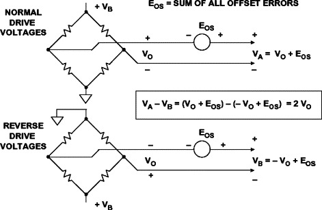
AC bridge excitation as shown in Figure 12.19 can effectively remove offset voltages in series with the bridge output. The concept is simple. The net bridge output voltage is measured under two conditions as shown. The first measurement yields a measurement VA, where VA is the sum of the desired bridge output voltage VO and the net offset error voltage EOS. The polarity of the bridge excitation is reversed, and a second measurement VB is made. Subtracting VB from VA yields 2VO, and the offset error term EOS cancels as shown.
Figure 12.19. AC excitation minimizes offset errors.
Obviously, this technique requires a highly accurate measurement ADC (such as the AD7730) as well as a microcontroller to perform the subtraction. If a ratiometric reference is desired, the ADC must also accommodate the changing polarity of the reference voltage. Again, the AD7730 includes this capability.
P-channel and N-channel MOSFETs can be configured as an AC bridge driver as shown in Figure 12.20. Dedicated bridge driver chips are also available, such as the Micrel MIC4427. Note that, because of the on-resistance of the MOSFETs, Kelvin sensing must be used in these applications. It is also important that the drive signals be nonoverlapping to prevent excessive MOSFET switching currents. The AD7730 ADC has on chip circuitry to generate the required nonoverlapping drive signals for AC excitation.
Figure 12.20. Simplified AC bridge drive circuit.

12.2. Amplifiers for Signal Conditioning
12.2.1. Introduction
This section examines the critical parameters of amplifiers for use in precision signal conditioning applications. Offset voltages for precision IC op-amps can be as low as 10 μV with corresponding temperature drifts of 0.1 μV/A° C. Chopper-stabilized op-amps provide offsets and offset voltage drifts that cannot be distinguished from noise. Open-loop gains greater than 1 million are common, along with common mode and power supply rejection ratios of the same magnitude. Applying these precision amplifiers while maintaining the amplifier performance can present significant challenges to a design engineer, that is, external passive component selection and PC board layout.
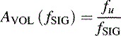
It is important to understand that DC open-loop gain, offset voltage, power supply rejection (PSR), and common mode rejection should not be the only considerations in selecting precision amplifiers. The AC performance of the amplifier is also important, even at “low” frequencies. Open-loop gain, PSR, and CMR all have relatively low corner frequencies, and therefore what may be considered “low” frequency may actually fall above these corner frequencies, increasing errors above the value predicted solely by the DC parameters. For example, an amplifier having a DC open-loop gain of 10 million and a unity-gain crossover frequency of 1 MHz has a corresponding corner frequency of 0.1 Hz! One must therefore consider the open-loop gain at the actual signal frequency. The relationship between the single-pole unity-gain crossover frequency, fu, the signal frequency, fSIG, and the open-loop gain AVOL(fSIG) (measured at the signal frequency) is given by (12.1)
In this example, the open-loop gain is 10 at 100 kHz, and 100,000 at 10 Hz. Loss of open-loop gain at the frequency of interest can introduce distortion, especially at audio frequencies. Loss of CMR or PSR at the line frequency or harmonics thereof can also introduce errors.
The challenge of selecting the right amplifier for a particular signal conditioning application has been complicated by the sheer proliferation of various types of amplifiers in various processes (bipolar, complementary bipolar, BiFET, CMOS, BiCMOS, etc.) and architectures (traditional op-amps, instrumentation amplifiers, chopper amplifiers, isolation amplifiers, etc.). In addition, a wide selection of precision amplifiers are now available that operate on single supply voltages, which complicates the design process even further because of the reduced signal swings and voltage input and output restrictions. Offset voltage and noise are now a more significant portion of the input signal. Selection guides and parametric search engines that can simplify this process somewhat are available on the Internet (www.analog.com) as well as on CD-ROM. Other manufacturers have similar information available.
In this section, we will first look at some key performance specifications for precision op-amps (Figure 12.21). Other amplifiers will then be examined such as instrumentation amplifiers, chopper amplifiers, and isolation amplifiers. The implications of single-supply operation will be discussed in detail because of its significance in today's designs, which often operate from batteries or other low-power sources.
Figure 12.21. Amplifiers for signal conditioning.

12.2.2. Precision Op-Amp Characteristics
12.2.2.1. Input Offset Voltage
Input offset voltage error is usually one of the largest error sources for precision amplifier circuit designs. However, it is a systemic error and can usually be dealt with by using a manual offset null trim or by system calibration techniques using a microcontroller or microprocessor. Both solutions carry a cost penalty, and today's precision op-amps offer initial offset voltages as low as 10 μV for bipolar devices, and far less for chopper-stabilized amplifiers. With low-offset amplifiers, it is possible to eliminate the need for manual trims or system calibration routines.
Measuring input offset voltages of a few microvolts requires that the test circuit does not introduce more error than the offset voltage itself. Figure 12.22 shows a circuit for measuring offset voltage. The circuit amplifies the input offset voltage by the noise gain (1001). The measurement is made at the amplifier output using an accurate digital voltmeter. The offset referred to the input (RTI) is calculated by dividing the output voltage by the noise gain. The small source resistance seen at R1||R2 results in negligible bias current contribution to the measured offset voltage. For example, 2-nA bias current flowing through the 10-Ω resistor produces a 0.02-μV error referred to the input.
Figure 12.22. Measuring input offset voltage.

As simple as it looks, this circuit may give inaccurate results. The largest potential source of error comes from parasitic thermocouple junctions formed where two different metals are joined. The thermocouple voltage formed by temperature difference between two junctions can range from 2 μV/A° C to more than 40 μV/A° C. Note that in the circuit additional resistors have been added to the noninverting input in order to exactly match the thermocouple junctions in the inverting input path.
The accuracy of the measurement depends on the mechanical layout of the components and how they are placed on the PC board. Keep in mind that the two connections of a component such as a resistor create two equal but opposite polarity thermoelectric voltages (assuming they are connected to the same metal, such as the copper trace on a PC board) that cancel each other assuming both are at exactly the same temperature. Clean connections and short lead lengths help to minimize temperature gradients and increase the accuracy of the measurement.
Airflow should be minimal so that all the thermocouple junctions stabilize at the same temperature. In some cases, the circuit should be placed in a small closed container to eliminate the effects of external air currents. The circuit should be placed flat on a surface so that convection currents flow up and off the top of the board, not across the components as would be the case if the board was mounted vertically.
Measuring the offset voltage shift over temperature is an even more demanding challenge. Placing the printed circuit board containing the amplifier being tested in a small box or plastic bag with foam insulation prevents the temperature chamber air current from causing thermal gradients across the parasitic thermocouples. If cold testing is required, a dry nitrogen purge is recommended. Localized temperature cycling of the amplifier itself using a Thermostream-type heater/cooler may be an alternative. However, these units tend to generate quite a bit of airflow, which can be troublesome.
In addition to temperature-related drift, the offset voltage of an amplifier changes as time passes. This aging effect is generally specified as long-term stability in microvolts per month, or microvolts per 1000 hours, but this is misleading. Since aging is a “drunkard's walk” phenomenon, it is proportional to the square root of the elapsed time. An aging rate of 1 μV/1000 hours becomes about 3 μV/year, not 9 μV/year. Long-term stability of the OP177 and the AD707 is approximately 0.3 μV/month. This refers to a time period after the first 30 days of operation. Excluding the initial hour of operation, changes in the offset voltage of these devices during the first 30 days of operation are typically less than 2 μV.
As a general rule of thumb, it is prudent to control amplifier offset voltage by device selection whenever possible, but sometimes trim may be desired. Many precision op-amps have pins available for optional offset null. Generally, two pins are joined by a potentiometer, and the wiper goes to one of the supplies through a resistor as shown in Figure 12.23. If the wiper is connected to the wrong supply, the op-amp will probably be destroyed, so the data sheet instructions must be carefully observed! The range of offset adjustment in a precision op-amp should be no more than two or three times the maximum offset voltage of the lowest grade device, in order to minimize the sensitivity of these pins. The voltage gain of an op-amp between its offset adjustment pins and its output may actually be greater than the gain at its signal inputs! It is therefore very important to keep these pins free of noise. It is inadvisable to have long leads from an op-amp to a remote potentiometer. To minimize any offset error due to supply current, connect R1 directly to the pertinent device supply pin, such as pin 7 shown in the diagram.
Figure 12.23. OP177/AD707 offset adjustment pins.

It is important to note that the offset drift of an op-amp with temperature will vary with the setting of its offset adjustment. In most cases a bipolar op-amp will have minimum drift at minimum offset. The offset adjustment pins should therefore be used only to adjust the op-amp's own offset, not to correct any system offset errors, since this would be at the expense of increased temperature drift. The drift penalty for a JFET input op-amp is much worse than for a bipolar input and is on the order of 4 μV/A° C for each millivolt of nulled offset voltage. It is generally better to control the offset voltage by proper selection of devices and device grades. Dual, triple, quad, and single op-amps in small packages do not generally have null capability because of pin count limitations, and offset adjustments must be done elsewhere in the system when using these devices. This can be accomplished with minimal impact on drift by a universal trim, which sums a small voltage into the input.
12.2.2.2. Input Offset Voltage and Input Bias Current Models
Thus far, we have considered only the op-amp input offset voltage. However, the input bias currents also contribute to offset error as shown in the generalized model of Figure 12.24. It is useful to refer all offsets to the op-amp input (RTI) so that they can be easily compared with the input signal. The equations in the diagram are given for the total offset voltage referred to input (RTI) and referred to output (RTO).
Figure 12.24. Op-amp total offset voltage model.

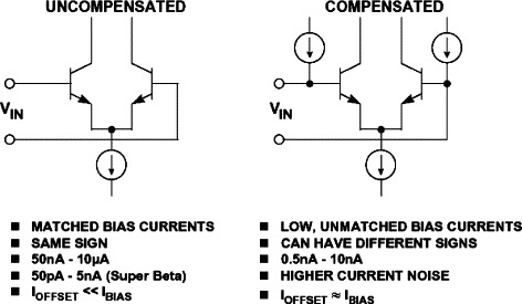
For a precision op-amp having a standard bipolar input stage using either PNPs or NPNs, the input bias currents are typically 50 nA to 400 nA and are well matched. By making R3 equal to the parallel combination of R1 and R2, their effect on the net RTI and RTO offset voltage is approximately canceled, thus leaving the offset current, that is, the difference between the input currents as an error. This current is usually an order of magnitude lower than the bias current specification. This scheme, however, does not work for bias-current compensated bipolar op-amps (such as the OP177 and the AD707) as shown in Figure 12.25. Bias-current compensated input stages have most of the good features of the simple bipolar input stage: low offset and drift, and low voltage noise. Their bias current is low and fairly stable over temperature. The additional current sources reduce the net bias currents typically to between 0.5 nA and 10 nA. However, the signs of the + and – input bias currents may or may not be the same, and they are not well matched but are very low. Typically, the specification for the offset current (the difference between the + and – input bias currents) in bias-current compensated op-amps is generally about the same as the individual bias currents. In the case of the standard bipolar differential pair with no bias-current compensation, the offset current specification is typically 5 to 10 times lower than the bias current specification.
Figure 12.25. Input bias-current compensated op-amps.
12.2.2.3. DC Open-Loop Gain Nonlinearity
It is well understood that, in order to maintain accuracy, a precision amplifier's DC open-loop gain, AVOL, should be high. This can be seen by examining the equation for the closed-loop gain: (12.2)
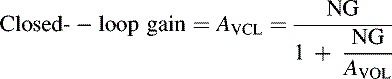
Noise gain (NG) is simply the gain seen by a small voltage source in series with the op-amp input and is also the amplifier signal gain in the noninverting mode. If AVOL in these equation is infinite, the closed-loop gain is exactly equal to the noise gain. However, for finite values of AVOL, there is a closed-loop gain error given by the equation: (12.3)
![]()
Notice from the equation that the percent gain error is directly proportional to the noise gain, therefore the effects of finite AVOL are less for low gain. The first example in Figure 12.26 where the noise gain is 1000 shows that, for an open-loop gain of 2 million, there is a gain error of about 0.05%. If the open-loop gain stays constant over temperature and for various output loads and voltages, the gain error can be calibrated out of the measurement, and there is then no overall system gain error.
Figure 12.26. Changes in DC open-loop gain cause closed loop gain uncertainty.

If, however, the open-loop gain changes, the closed-loop gain will also change, thereby introducing a gain uncertainty. In the second example in the figure, an AVOL decrease to 300,000 produces a gain error of 0.33%, introducing a gain uncertainty of 0.28% in the closed-loop gain. In most applications, using the proper amplifier, the resistors around the circuit will be the largest source of gain error.
Changes in the output voltage level and the output loading are the most common causes of changes in the open-loop gain of op-amps. A change in open-loop gain with signal level produces nonlinearity in the closed-loop gain transfer function which cannot be removed during system calibration. Most op-amps have fixed loads, so AVOL changes with load are not generally important. However, the sensitivity of AVOL to output signal level may increase for higher load currents.
The severity of the nonlinearity varies widely from device type to device type and is generally not specified on the data sheet. The minimum AVOL is always specified, and choosing an op-amp with a high AVOL will minimize the probability of gain nonlinearity errors. Gain nonlinearity can come from many sources, depending on the design of the op-amp. One common source is thermal feedback. If temperature shift is the sole cause of the nonlinearity error, it can be assumed that minimizing the output loading will help. To verify this, the nonlinearity is measured with no load and then compared to the loaded condition.
An oscilloscope X-Y display test circuit for measuring DC open-loop gain nonlinearity is shown in Figure 12.27. The same precautions previously discussed relating to the offset voltage test circuit must be observed in this circuit. The amplifier is configured for a signal gain of −1. The open-loop gain is defined as the change in output voltage divided by the change in the input offset voltage. However, for large values of AVOL, the offset may change only a few microvolts over the entire output voltage swing. Therefore the divider consisting of the 10-Ω resistor and RG (1 MΩ) forces the voltage VY to be (12.4)
Figure 12.27. Circuit measures open-loop gain nonlinearity.
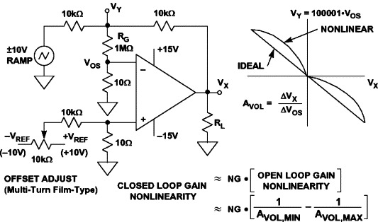
The value of RG is chosen to give measurable voltages at VY depending on the expected values of VOS.
The ±10-V ramp generator output is multiplied by the signal gain, −1, and forces the op-amp output voltage VX to swing from +10V to −10V. Because of the gain factor applied to the offset voltage, the offset adjust potentiometer is added to allow the initial output offset to be set to zero. The resistor values chosen will null an input offset voltage of up to ±10 mV. Stable 10-V voltage references should be used at each end of the potentiometer to prevent output drift. Also, the frequency of the ramp generator must be quite low, probably no more than a fraction of 1 Hz because of the low corner frequency of the open-loop gain (0.1 Hz for the OP177).
The plot on the right-hand side of Figure 12.27 shows VY plotted against VX. If there is no gain nonlinearity the graph will have a constant slope, and AVOL is calculated as follows: (12.5)
If there is nonlinearity, AVOL will vary as the output signal changes. The approximate open-loop gain nonlinearity is calculated based on the maximum and minimum values of AVOL over the output voltage range: (12.6)
The closed-loop gain nonlinearity is obtained by multiplying the open-loop gain nonlinearity by the noise gain, NG: (12.7)

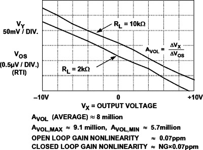
In the ideal case, the plot of VOS versus VX would have a constant slope, and the reciprocal of the slope is the open-loop gain, AVOL. A horizontal line with zero slope would indicate infinite open-loop gain. In an actual op-amp, the slope may change across the output range because of nonlinearity, thermal feedback, and the like. In fact, the slope can even change sign.
Figure 12.28 shows the VY (and VOS) versus VX plot for the OP177 precision op-amp. The plot is shown for two different loads, 2 kΩ and 10 kΩ. The reciprocal of the slope is calculated based on the end points, and the average AVOL is about 8 million. The maximum and minimum values of AVOL across the output voltage range are measured to be approximately 9.1 million and 5.7 million, respectively. This corresponds to an open-loop gain nonlinearity of about 0.07 ppm. Thus, for a noise gain of 100, the corresponding closed-loop gain nonlinearity is about 7 ppm.
Figure 12.28. OP177 gain nonlinearity.
12.2.2.4. Op-Amp Noise
The three noise sources in an op-amp circuit are the voltage noise of the op-amp, the current noise of the op-amp (there are two uncorrelated sources, one in each input), and the Johnson noise of the resistances in the circuit. Op-amp noise has two components, “white” noise at medium frequencies and low-frequency “1/f” noise, whose spectral density is inversely proportional to the square root of the frequency. It should be noted that, though both the voltage and the current noise may have the same characteristic behavior, in a particular amplifier the 1/f corner frequency is not necessarily the same for voltage and current noise (it is usually specified for the voltage noise as shown in Figure 12.29).
Figure 12.29. Input voltage noise for OP177/AD707.
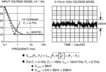
The low-frequency noise is generally known as 1/f noise (the noise power obeys a 1/f law—the noise voltage or noise current is proportional to 1/f). The frequency at which the 1/f noise spectral density equals the white noise is known as the 1/f corner frequency, FC, and is a figure of merit for an op-amp, with low corner frequencies indicating better performance. Values of 1/f corner frequency vary from less than 1 Hz for high-accuracy bipolar op-amps like the OP177/AD707, several hundred Hz for the AD743/745 FET-input op-amps, to several thousands of Hz for some high-speed op-amps where process compromises favor high speed rather than low-frequency noise.
For the OP177/AD707 shown in Figure 12.29, the 1/f corner frequency is 0.7 Hz, and the white noise is 10 nV/√Hz. The low-frequency 1/f noise is often expressed as the peak-to-peak noise in the bandwidth 0.1 Hz to 10 Hz as shown in the scope photo in Figure 12.29. Note that this noise ultimately limits the resolution of a precision measurement system because the bandwidth up to 10 Hz is usually the bandwidth of most interest. The equation for the total rms noise, Vn,rms, in the bandwidth FL to FH is given by the equation (12.8)
 where vNW is the noise spectral density in the “white-noise” region (usually specified at a frequency of 1 kHz), FC is the 1/f corner frequency, and FL and FH are the measurement bandwidths of interest. In the example shown, the 0.1 Hz to 10 Hz noise is calculated to be 36-nV rms,
or approximately 238-nV peak to peak, which closely agrees with the scope photo on the right (a factor of 6.6 is generally
used to convert rms values to peak-to-peak values).
where vNW is the noise spectral density in the “white-noise” region (usually specified at a frequency of 1 kHz), FC is the 1/f corner frequency, and FL and FH are the measurement bandwidths of interest. In the example shown, the 0.1 Hz to 10 Hz noise is calculated to be 36-nV rms,
or approximately 238-nV peak to peak, which closely agrees with the scope photo on the right (a factor of 6.6 is generally
used to convert rms values to peak-to-peak values).
It should be noted that, at higher frequencies, the term in the equation containing the natural logarithm becomes insignificant, and the expression for the rms noise becomes
![]()
![]()
However, some op-amps (such as the OP07 and OP27) have voltage noise characteristics that increase slightly at high frequencies. The voltage noise versus frequency curve for op-amps should therefore be examined carefully for flatness when calculating high-frequency noise using this approximation.
At very low frequencies when operating exclusively in the 1/f region, FC ≫ (FH – FL), and the expression for the rms noise reduces to (12.10)

Note that there is no way of reducing this 1/f noise by filtering if operation extends to DC. Making FH = 0.1 Hz and FL = 0.001 still yields an rms 1/f noise of about 18-nV rms, or 119-nV peak to peak.
The point is that averaging the results of a large number of measurements taken over a long period of time has practically no effect on the error produced by 1/f noise. The only method of reducing it further is to use a chopper-stabilized op-amp which does not pass the low-frequency noise components.
A generalized noise model for an op-amp is shown in Figure 12.30. All uncorrelated noise sources add as a root-sum-of-squares manner, that is, noise voltages V1, V2, and V3 give a result of (12.11)
![]()
Figure 12.30. Op-amp noise model.

Thus, any noise voltage that is more than four or five times any of the others is dominant, and the others may generally be ignored. This simplifies noise analysis.
In this diagram, the total noise of all sources is shown referred to the input. The RTI noise is useful because it can be compared directly to the input signal level. The total noise referred to the output is obtained by simply multiplying the RTI noise by the noise gain.
The diagram assumes that the feedback network is purely resistive. If it contains reactive elements (usually capacitors), the noise gain is not constant over the bandwidth of interest, and more complex techniques must be used to calculate the total noise (see in particular, Reference 12). However, for precision applications where the feedback network is most likely to be resistive, the equations are valid.
Notice that the Johnson noise voltage associated with the three resistors has been included. All resistors have a Johnson noise of 4 kTBR, where k is Boltzmann's constant (1.38 × 10⁻²³ J/K), T is the absolute temperature, B is the bandwidth in hertz, and R is the resistance in ohms. A simple relationship which is easy to remember is that a 1000-Ω resistor generates a Johnson noise of 4 nV/√Hz at 25A° C.
The voltage noise of various op-amps may vary from under 1 nV/√Hz to 20 nV/√Hz, or even more. Bipolar input op-amps tend to have lower voltage noise than JFET input ones, although it is possible to make JFET input op-amps with low-voltage noise (such as the AD743/AD745), at the cost of large input devices and hence large (∼20-pF) input capacitance. Current noise can vary much more widely, from around 0.1 fA/Hz (in JFET input electrometer op-amps) to several pA/√Hz (in high-speed bipolar op-amps). For bipolar or JFET input devices where all the bias current flows into the input junction, the current noise is simply the Schottky (or shot) noise of the bias current. The shot noise spectral density is simply 2IBq amps/√Hz, where IB is the bias current (in amps) and q is the charge on an electron (1.6 × 10⁻¹⁹ C). It cannot be calculated for bias-compensated or current feedback op-amps where the external bias current is the difference between two internal current sources.
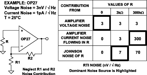
Current noise is only important when it flows through an impedance and in turn generates a noise voltage. The equation shown in Figure 12.30 shows how the current noise flowing in the resistors contributes to the total noise. The choice of a low-noise op-amp therefore depends on the impedances around it. Consider an OP27, a bias-compensated op-amp with low voltage noise (3 nV/√Hz), but quite high current noise (1 pA/√Hz) as shown in the schematic of Figure 12.31. With zero source impedance, the voltage noise dominates. With a source resistance of 3 kΩ, the current noise (1 pA/√Hz) flowing in 3 kΩ will equal the voltage noise, but the Johnson noise of the 3-kΩ resistor is 7 nV/√Hz and so is dominant. With a source resistance of 300 kΩ, the effect of the current noise increases a hundredfold to 300 nV/√Hz, while the voltage noise is unchanged, and the Johnson noise (which is proportional to the square root of the resistance) increases tenfold. Here, the current noise dominates.
Figure 12.31. Different noise sources dominate at different source impedances.
The previous example shows that the choice of a low-noise op-amp depends on the source impedance of the input signal, and at high impedances, current noise always dominates. This is shown in Figure 12.32 for several bipolar (OP07, OP27, 741) and JFET (AD645, AD743, AD744) op-amps.
Figure 12.32. Different amplifiers are best at different source impedance levels.
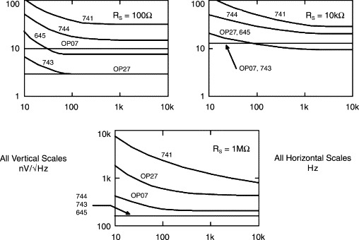
For low-impedance circuitry (generally <1 kΩ), amplifiers with low voltage noise, such as the OP27 will be the obvious choice, and their comparatively large current noise will not affect the application. At medium resistances, the Johnson noise of resistors is dominant, while at very high resistances, we must choose an op-amp with the smallest possible current noise, such as the AD549 or AD645.
Until recently, BiFET amplifiers (with JFET inputs) tended to have comparatively high voltage noise (though very low current noise), and thus were more suitable for low-noise applications in high rather than low-impedance circuitry. The AD645, AD743, and AD745 have very low values of both voltage and current noise. The AD645 specifications at 10 kHz are 10 nV/√Hz and 0.6 fA/√Hz, and the AD743/ AD745 specifications at 10 kHz are 2.0 nV/√Hz and 6.9 fA/√Hz. These make possible the design of low-noise amplifier circuits which have low noise over a wide range of source impedances.
12.2.2.5. Common Mode Rejection and Power Supply Rejection
If a signal is applied equally to both inputs of an op-amp so that the differential input voltage is unaffected, the output should not be affected. In practice, changes in common mode voltage will produce changes in the output. The common mode rejection ratio or CMRR is the ratio of the common mode gain to the differential mode gain of an op-amp. For example, if a differential input change of Y volts will produce a change of 1V at the output, and a common mode change of X volts produces a similar change of 1V, then the CMRR is X/Y. It is normally expressed in decibels, and typical LF values are between 70 and 120 dB. When expressed in decibels, it is generally referred to as common mode rejection (CMR). At higher frequencies, CMR deteriorates—many op-amp data sheets show a plot of CMR versus frequency as shown in Figure 12.33 for the OP177/AD707 precision op-amps.
Figure 12.33. OP177/AD707 common mode rejection (CMR).

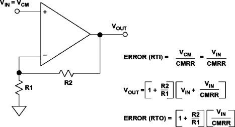
CMRR produces a corresponding output offset voltage error in op-amps configured in the noninverting mode as shown in Figure 12.34. Op-amps configured in the inverting mode have no CMRR output error because both inputs are at ground or virtual ground, so there is no common mode voltage, only the offset voltage of the amplifier if unnulled.
Figure 12.34. Calculating offset error due to common mode rejection ratio (CMRR).
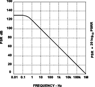
If the supply of an op-amp changes, its output should not, but it will. The specification of power supply rejection ratio or PSRR is defined similarly to the definition of CMRR. If a change of X volts in the supply produces the same output change as a differential input change of Y volts, then the PSRR on that supply is X/Y. When the ratio is expressed in decibels, it is generally referred to as power supply rejection, or PSR. The definition of PSRR assumes that both supplies are altered equally in opposite directions—otherwise the change will introduce a common mode change as well as a supply change, and the analysis becomes considerably more complex. It is this effect which causes apparent differences in PSRR between the positive and negative supplies. In the case of single-supply op-amps, PSR is generally defined with respect to the change in the positive supply. Many single supply op-amps have separate PSR specifications for the positive and negative supplies. The PSR of the OP177/AD707 is shown in Figure 12.35.
Figure 12.35. OP177/AD707 power supply rejection (PSR).
The PSRR of op-amps is frequency dependent, therefore power supplies must be well decoupled as shown in Figure 12.36. At low frequencies, several devices may share a 10–50-μF capacitor on each supply, provided it is no more than 10 cm (PC track distance) from any of them. At high frequencies, each IC must have every supply decoupled by a low-inductance capacitor (0.1 μF or so) with short leads and PC tracks. These capacitors must also provide a return path for HF currents in the op-amp load. Decoupling capacitors should be connected to a low-impedance large-area ground plane with minimum lead lengths. Surface mount capacitors minimize lead inductance and are a good choice.
Figure 12.36. Proper low- and high-frequency decoupling techniques for op-amps.

12.2.3. Amplifier DC Error Budget Analysis
A room temperature error budget analysis for the OP177A op-amp is shown in Figure 12.37. The amplifier is connected in the inverting mode with a signal gain of 100. The key data sheet specifications are also shown in the diagram. We assume an input signal of 100-mV full scale which corresponds to an output signal of 10V. The various error sources are normalized to full scale and expressed in parts per million (ppm). Note: Parts per million error = Fractional error × 106 = Percent error × 104.
Figure 12.37. Precision op amp (OP177A) DC error budget.

Note that the offset errors due to VOS and IOS and the gain error due to finite AVOL can be removed with a system calibration. However, the error due to open-loop gain nonlinearity cannot be removed with calibration and produces a relative accuracy error, often called resolution error.
The second contributor to resolution error is the 1/f noise. This noise is always present and adds to the uncertainty of the measurement. The overall relative accuracy of the circuit at room temperature is 9 ppm which is equivalent to approximately 17 bits of resolution.
12.2.4. Single-Supply Op-Amps
Over the last several years, single-supply operation has become an increasingly important requirement because of market requirements (Figure 12.38). Automotive, set-top box, camera/camcorder, PC, and laptop computer applications are demanding IC vendors to supply an array of linear devices that operate on a single supply rail, with the same performance of dual-supply parts. Power consumption is now a key parameter for line- or battery-operated systems, and in some instances, more important than cost. This makes low-voltage/low-supply current operation critical; at the same time, however, accuracy and precision requirements have forced IC manufacturers to meet the challenge of “doing more with less” in their amplifier designs.
Figure 12.38. Single-supply amplifiers.

In a single-supply application, the most immediate effect on the performance of an amplifier is the reduced input and output signal range. As a result of these lower input and output signal excursions, amplifier circuits become more sensitive to internal and external error sources. Precision amplifier offset voltages on the order of 0.1 mV are less than a 0.04 LSB error source in a 12-bit, 10-V full-scale system. In a single-supply system, however, a “rail-to-rail” precision amplifier with an offset voltage of 1 mV represents a 0.8 LSB error in a 5-V full-scale system, and 1.6 LSB error in a 2.5-V full-scale system.
To keep battery current drain low, larger resistors are usually used around the op-amp. Since the bias current flows through these larger resistors, they can generate offset errors equal to or greater than the amplifier's own offset voltage.
Gain accuracy in some low-voltage single-supply devices is also reduced, so device selection needs careful consideration. Many amplifiers having open-loop gains in the millions typically operate on dual supplies, for example, the OP07 family types. However, many single-supply/rail-to-rail amplifiers for precision applications typically have open-loop gains between 25,000 and 30,000 under light loading (>10 kΩ). Selected devices, like the OP113/213/413 family, do have high open-loop gains (i.e., >1 M).
Many trade-offs are possible in the design of a single-supply amplifier circuit: speed versus power, noise versus power, precision versus speed and power, and so forth. Even if the noise floor remains constant (highly unlikely), the signal-to-noise ratio will drop as the signal amplitude decreases.
Besides these limitations, many other design considerations that are otherwise minor issues in dual-supply amplifiers now become important. For example, signal-to-noise (SNR) performance degrades as a result of reduced signal swing. “Ground reference” is no longer a simple choice, as one reference voltage may work for some devices but not others. Amplifier voltage noise increases as operating supply current drops, and bandwidth decreases. Achieving adequate bandwidth and required precision with a somewhat limited selection of amplifiers presents significant system design challenges in single-supply, low-power applications.
Most circuit designers take “ground” reference for granted. Many analog circuits scale their input and output ranges about a ground reference. In dual-supply applications, a reference that splits the supplies (0V) is very convenient, as there is equal supply headroom in each direction, and 0V is generally the voltage on the low-impedance ground plane.
In single-supply/rail-to-rail circuits, however, the ground reference can be chosen anywhere within the supply range of the circuit, since there is no standard to follow. The choice of ground reference depends on the type of signals processed and the amplifier characteristics. For example, choosing the negative rail as the ground reference may optimize the dynamic range of an op-amp whose output is designed to swing to 0V. On the other hand, the signal may require level shifting in order to be compatible with the input of other devices (such as ADCs) that are not designed to operate at 0-V input.
Early single-supply “zero-in, zero-out” amplifiers were designed on bipolar processes that optimized the performance of the NPN transistors. The PNP transistors were either lateral or substrate PNPs with much less bandwidth than the NPNs. Fully complementary processes are now required for the new breed of single-supply/rail-to-rail operational amplifiers. These new amplifier designs do not use lateral or substrate PNP transistors within the signal path, but incorporate parallel NPN and PNP input stages to accommodate input signal swings from ground to the positive supply rail. Furthermore, rail-to-rail output stages are designed with bipolar NPN and PNP common-emitter, or N-channel/P-channel common-source amplifiers whose collector/emitter saturation voltage or drain-source channel on-resistance determine output signal swing as a function of the load current.
The characteristics of a single-supply amplifier input stage (common mode rejection, input offset voltage and its temperature coefficient, and noise) are critical in precision, low-voltage applications. Rail-to-rail input operational amplifiers must resolve small signals, whether their inputs are at ground or in some cases near the amplifier's positive supply. Amplifiers having a minimum of 60-dB common mode rejection over the entire input common mode voltage range from 0V to the positive supply are good candidates. It is not necessary that amplifiers maintain common mode rejection for signals beyond the supply voltages: What is required is that they do not self-destruct for momentary overvoltage conditions. Furthermore, amplifiers that have offset voltages less than 1 mV and offset voltage drifts less than 2 μV/° C are also very good candidates for precision applications. Since input signal dynamic range and SNR are equally if not more important than output dynamic range and SNR, precision single-supply/rail-to-rail operational amplifiers should have noise levels referred to input less than 5 μVp-p in the 0.1 Hz to 10 Hz band.
The need for rail-to-rail amplifier output stages is driven by the need to maintain wide dynamic range in low-supply voltage applications. A single-supply/rail-to-rail amplifier should have output voltage swings which are within at least 100 mV of either supply rail (under a nominal load). The output voltage swing is very dependent on output stage topology and load current. The voltage swing of a good output stage should maintain its rated swing for loads down to 10 kΩ. The smaller the VOL and the larger the VOH, the better. System parameters, such as “zero-scale” or “full-scale” output voltage, should be determined by an amplifier's VOL (for zero scale) and VOH (for full scale).
Since the majority of single-supply data acquisition systems require at least 12- to 14-bit performance, amplifiers that exhibit an open-loop gain greater than 30,000 for all loading conditions are good choices in precision applications.
12.2.4.1. Single-Supply Op-Amp Input Stages
There is some demand for op-amps whose input common mode voltage includes both supply rails. Such a feature is undoubtedly useful in some applications, but engineers should recognize that there are relatively few applications where it is absolutely essential. These should be carefully distinguished from the many applications where common mode range close to the supplies or one that includes one of the supplies is necessary, but input rail-to-rail operation is not.
In many single-supply applications, it is required that the input go to only one of the supply rails (usually ground). High-side or low-side sensing applications are good examples of this. Amplifiers that will handle 0-V inputs are relatively easily designed using PNP differential pairs (or N-channel JFET pairs) as shown in Figure 12.39. The input common mode range of such an op-amp extends from about 200 mV below the negative supply to within about 1V of the positive supply.
Figure 12.39. PNP or N-channel JFET stages allow input signal to go to the negative rail.

The input stage could also be designed with NPN transistors (or P-channel JFETs), in which case the input common mode range would include the positive rail and to within about 1V of the negative rail. This requirement typically occurs in applications such as high-side current sensing, a low-frequency measurement application. The OP282/OP482 input stage uses the P-channel JFET input pair whose input common mode range includes the positive rail. Other circuit topologies for high-side sensing (such as the AD626) use the precision resistors to attenuate the common mode voltage.
True rail-to-rail input stages require two long-tailed pairs (see Figure 12.40), one of NPN bipolar transistors (or N-channel JFETs), the other of PNP transistors (or P-channel JFETs). These two pairs exhibit different offsets and bias currents, so when the applied input common mode voltage changes, the amplifier input offset voltage and input bias current does also. In fact, when both current sources remain active throughout the entire input common mode range, amplifier input offset voltage is the average offset voltage of the NPN pair and the PNP pair. In those designs where the current sources are alternatively switched off at some point along the input common mode voltage, amplifier input offset voltage is dominated by the PNP pair offset voltage for signals near the negative supply, and by the NPN pair offset voltage for signals near the positive supply. It should be noted that true rail-to-rail input stages can also be constructed from CMOS transistors as in the case of the OP250/450 and the AD8531/8532/8534.
Figure 12.40. True rail-to-rail input stage.

Amplifier input bias current, a function of transistor current gain, is also a function of the applied input common mode voltage. The result is relatively poor common mode rejection and a changing common mode input impedance over the common mode input voltage range, compared to familiar dual-supply devices. These specifications should be considered carefully when choosing a rail-rail input op-amp, especially for a noninverting configuration. Input offset voltage, input bias current, and even CMR may be quite good over part of the common mode range, but much worse in the region where operation shifts between the NPN and PNP devices and vice versa.
True rail-to-rail amplifier input stage designs must transition from one differential pair to the other differential pair somewhere along the input common mode voltage range. Some devices like the OP191/291/491 family and the OP279 have a common mode crossover threshold at approximately 1V below the positive supply. The PNP differential input stage is active from about 200 mV below the negative supply to within about 1V of the positive supply. Over this common mode range, amplifier input offset voltage, input bias current, CMR, input noise voltage/current are primarily determined by the characteristics of the PNP differential pair. At the crossover threshold, however, amplifier input offset voltage becomes the average offset voltage of the NPN/PNP pairs and can change rapidly. Also, amplifier bias currents, dominated by the PNP differential pair over most of the input common mode range, change polarity and magnitude at the crossover threshold when the NPN differential pair becomes active.
Op amps like the OP184/284/484 utilize a rail-to-rail input stage design where both NPN and PNP transistor pairs are active throughout the entire input common mode voltage range, and there is no common mode crossover threshold. Amplifier input offset voltage is the average offset voltage of the NPN and the PNP stages. Amplifier input offset voltage exhibits a smooth transition throughout the entire input common mode range because of careful laser trimming of the resistors in the input stage. In the same manner, through careful input stage current balancing and input transistor design, amplifier input bias currents also exhibit a smooth transition throughout the entire common mode input voltage range. The exception occurs at the extremes of the input common mode range, where amplifier offset voltages and bias currents increase sharply due to the slight forward-biasing of parasitic p-n junctions. This occurs for input voltages within approximately 1V of either supply rail.
When both differential pairs are active throughout the entire input common mode range, amplifier transient response is faster through the middle of the common mode range by as much as a factor of 2 for bipolar input stages and by a factor of √2 for JFET input stages. Input stage transconductance determines the slew rate and the unity-gain crossover frequency of the amplifier, hence response time degrades slightly at the extremes of the input common mode range when either the PNP stage (signals approaching the positive supply rail) or the NPN stage (signals approaching the negative supply rail) are forced into cutoff. The thresholds at which the transconductance changes occur are approximately within 1V of either supply rail, and the behavior is similar to that of the input bias currents.
Applications that require true rail-rail inputs should therefore be carefully evaluated, and the amplifier chosen to ensure that its input offset voltage, input bias current, common mode rejection, and noise (voltage and current) are suitable.
12.2.4.2. Single-Supply Op-Amp Output Stages
The earliest IC op-amp output stages were NPN emitter-followers with NPN current sources or resistive pull-downs, as shown in the left-hand diagram of Figure 12.41. Naturally, the slew rates were greater for positive-going than for negative-going signals. While all modern op-amps have push/pull output stages of some sort, many are still asymmetrical and have a greater slew rate in one direction than the other. Asymmetry tends to introduce distortion on AC signals and generally results from the use of IC processes with faster NPN than PNP transistors. It may also result in the ability of the output to approach one supply more closely than the other.
Figure 12.41. Traditional output stages.

In many applications, the output is required to swing only to one rail, usually the negative rail (i.e., ground in single-supply systems). A pull-down resistor to the negative rail will allow the output to approach that rail (provided the load impedance is high enough or is also grounded to that rail), but only slowly. Using an FET current source instead of a resistor can speed things up, but this adds complexity.
With new complementary bipolar (CB) processes, well-matched high-speed PNP and NPN transistors are available. The complementary emitter-follower output stage shown in the right-hand diagram of Figure 12.41 has many advantages including low output impedance. However, the output can only swing within about one VBE drop of either supply rail. An output swing of +1V to +4V is typical of such stages when operated on a single +5-V supply.
The complementary common-emitter/common-source output stages shown in Figure 12.42 allow the output voltage to swing much closer to the output rails, but these stages have higher open-loop output impedance than the emitter follower-based stages. In practice, however, the amplifier's open-loop gain and local feedback produce an apparent low-output impedance, particularly at frequencies below 10 Hz.
Figure 12.42. “Almost” rail-to-rail output structures.

The complementary common emitter output stage using BJTs (left-hand diagram in Figure 12.42) cannot swing completely to the rails, but only to within the transistor saturation voltage (VCESAT) of the rails. For small amounts of load current (less than 100 μA), the saturation voltage may be as low as 5 to 10 mV, but for higher load currents, the saturation voltage can increase to several hundred millivolts (for example, 500 mV at 50 mA).
On the other hand, an output stage constructed of CMOS FETs can provide nearly true rail-to-rail performance, but only under no-load conditions. If the output must source or sink current, the output swing is reduced by the voltage dropped across the FETs internal “on” resistance (typically, 100Ω for precision amplifiers, but can be less than 10Ω for high-current drive CMOS amplifiers).
For these reasons, it is apparent that there is no such thing as a true rail-to-rail output stage, hence the title of Figure 12.42 (“almost” rail-to-rail output stages).
Figure 12.43 summarizes the performance characteristics of a number of single-supply op-amps suitable for some precision applications. The devices are listed in order of increasing supply current. Single, dual, and quad versions of each op-amp are available, so the supply current is the normalized ISY/amplifier for comparison. The input and output voltage ranges (VS = +5V) are also supplied in the table. The “0, 4V” inputs are PNP pairs, with the exception of the AD820/822/824 which use N-channel JFETs. Output stages having voltage ranges designated “5 mV, 4V” are NPN emitter-followers with current source pull-downs (OP193/293/493, OP113/213/413). Output stages designated “R/R” use CMOS common source stages (OP181/281/481) or CB common emitter stages (OP196/296/496, OP191/291/491, AD820/822/824, OP184/284/484).
Figure 12.43. Precision single-supply op-amp performance characteristics.

In summary, the following points should be considered when selecting amplifiers for single-supply/rail-to-rail applications.
First, input offset voltage and input bias currents are a function of the applied input common mode voltage (for true rail-to-rail input op-amps). Circuits using this class of amplifiers should be designed to minimize resulting errors. An inverting amplifier configuration with a false ground reference at the noninverting input prevents these errors by holding the input common mode voltage constant. If the inverting amplifier configuration cannot be used, then amplifiers like the OP184/284/OP484 which do not exhibit any common mode crossover thresholds should be used.
Second, since input bias currents are not always small and can exhibit different polarities, source impedance levels should be carefully matched to minimize additional input bias current-induced offset voltages and increased distortion. Again, consider using amplifiers that exhibit a smooth input bias current transition throughout the applied input common mode voltage.
Third, rail-to-rail amplifier output stages exhibit load-dependent gain that affects amplifier open-loop gain, and hence closed-loop gain accuracy. Amplifiers with open-loop gains greater than 30,000 for resistive loads less than 10 kΩ are good choices in precision applications. For applications not requiring full rail-rail swings, device families like the OP113/213/413 and OP193/293/493 offer DC gains of 200,000 or more.
Last, no matter what claims are made, rail-to-rail output voltage swings are functions of the amplifier's output stage devices and load current. The saturation voltage VCESAT), saturation resistance (RSAT) for bipolar output stages, and FET on-resistance for CMOS output stages, as well as load current all affect the amplifier output voltage swing.
12.2.4.3. Op-Amp Process Technologies
The wide variety of processes used to make op-amps are shown in Figure 12.44. The earliest op-amps were made using standard NPN-based bipolar processes. The PNP transistors available on these processes were extremely slow and were used primarily for current sources and level shifting.
Figure 12.44. Op-amp process technology summary.

The ability to produce matching high-speed PNP transistors on a bipolar process added great flexibility to op-amp circuit designs. These complementary bipolar processes are widely used in today's precision op-amps, as well as those requiring wide bandwidths. The high-speed PNP transistors have fts that are greater than one half the fts of the NPNs.
The addition of JFETs to the complementary bipolar process (CBFET) allows high-input impedance op-amps to be designed suitable for such applications as photodiode or electrometer preamplifiers.
CMOS op-amps, with a few exceptions, generally have relatively poor offset voltage, drift, and voltage noise. However, the input bias current is very low. They offer low power and cost, however, and improved performance can be achieved with BiFET or CBFET processes.
The addition of bipolar or complementary devices to a CMOS process (BiMOS or CBCMOS) adds great flexibility, better linearity, and low power. The bipolar devices are typically used for the input stage to provide good gain and linearity, and CMOS devices for the rail-to-rail output stage.
In summary, there is no single IC process which is optimum for all op-amps. Process selection and the resulting op-amp design depend on the targeted applications and ultimately should be transparent to the customer.
12.2.5. Instrumentation Amplifiers (In-Amps)
An instrumentation amplifier is a closed-loop gain block that has a differential input and an output that is single ended with respect to a reference terminal (see Figure 12.45). The input impedances are balanced and have high values, typically 109Ω or higher. Unlike an op-amp, which has its closed-loop gain determined by external resistors connected between its inverting input and its output, an in-amp employs an internal feedback resistor network that is isolated from its signal input terminals. With the input signal applied across the two differential inputs, gain is either preset internally or is user-set by an internal (via pins) or external gain resistor, which is also isolated from the signal inputs. Typical in-amp gain settings range from 1 to 10,000.
Figure 12.45. Instrumentation amplifier.

In order to be effective, an in-amp needs to be able to amplify microvolt-level signals, while simultaneously rejecting volts of common mode signal at its inputs. This requires that in-amps have very high common mode rejection (CMR): Typical values of CMR are 70 dB to over 100 dB, with CMR usually improving at higher gains.
It is important to note that a CMR specification for DC inputs alone is not sufficient in most practical applications. In industrial applications, the most common cause of external interference is pickup from the 50/60-Hz AC power mains. Harmonics of the power mains frequency can also be troublesome. In differential measurements, this type of interference tends to be induced equally onto both in-amp inputs. The interfering signal therefore appears as a common mode signal to the in-amp. Specifying CMR over frequency is more important than specifying its DC value. Imbalance in the source impedance can degrade the CMR of some in-amps. Analog Devices fully specifies in-amp CMR at 50/60 Hz with a source impedance imbalance of 1 kΩ.
Low-frequency CMR of op-amps, connected as subtractors as shown in Figure 12.46, generally is a function of the resistors around the circuit, not the op-amp. A mismatch of only 0.1% in the resistor ratios will reduce the DC CMR to approximately 66 dB. Another problem with the simple op-amp subtractor is that the input impedances are relatively low and are unbalanced between the two sides. The input impedance seen by V1 is R1, but the input impedance seen by V2 is R1′ + R2′. This configuration can be quite problematic in terms of CMR, since even a small source impedance imbalance (∼10Ω) will degrade the workable CMR.
Figure 12.46. Op-amp subtractor.
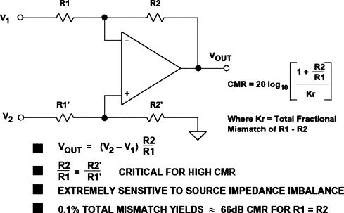
12.2.5.1. Instrumentation Amplifier Configurations
Instrumentation amplifier configurations are based on op-amps, but the simple subtractor circuit described previously lacks the performance required for precision applications. An in-amp architecture that overcomes some of the weaknesses of the subtractor circuit uses two op-amps as shown in Figure 12.47. This circuit is typically referred to as the two op-amp in-amp. Dual-IC op-amps are used in most cases for good matching. The circuit gain may be trimmed with an external resistor, RG. The input impedance is high, permitting the impedance of the signal sources to be high and unbalanced. The DC common mode rejection is limited by the matching of R1/R2 to R1′/R2′. If there is a mismatch in any of the four resistors, the DC common mode rejection is limited to (12.12)
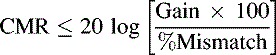
Figure 12.47. Two op-amp instrumentation amplifier.
There is an implicit advantage to this configuration due to the gain executed on the signal. This raises the CMR in proportion.
Integrated instrumentation amplifiers are particularly well suited to meeting the combined needs of ratio matching and temperature tracking of the gain-setting resistors. While thin film resistors fabricated on silicon have an initial tolerance of up to ±20%, laser trimming during production allows the ratio error between the resistors to be reduced to 0.01% (100 ppm). Furthermore, the tracking between the temperature coefficients of the thin film resistors is inherently low and is typically less than 3 ppm/A° C (0.0003%/A° C).
When dual supplies are used, VREF is normally connected directly to ground. In single-supply applications, VREF is usually connected to a low-impedance voltage source equal to one half the supply voltage. The gain from VREF to node A is R1/R2, and the gain from node A to the output is R2′/R1′. This makes the gain from VREF to the output equal to unity, assuming perfect ratio matching. Note that it is critical that the source impedance seen by VREF be low, otherwise CMR will be degraded.
One major disadvantage of this design is that common mode voltage input range must be traded off against gain. The amplifier A1 must amplify the signal at V1 by (12.13)
![]()
If R1 ≫ R2 (low gain in Figure 12.47), A1 will saturate if the common mode signal is too high, leaving no headroom to amplify the wanted differential signal. For high gains (R1 ≫ R2), there is correspondingly more headroom at node A allowing larger common mode input voltages.
The AC common mode rejection of this configuration is generally poor because the signal from V1 to VOUT has the additional phase shift of A1. In addition, the two amplifiers are operating at different closed-loop gains (and thus at different bandwidths). The use of a small trim capacitor C as shown in the diagram can improve the AC CMR somewhat.
A low gain (G = 2) single-supply two op-amp in-amp configuration results when RG is not used and is shown in Figure 12.48. The input common mode and differential signals must be limited to values that prevent saturation of either A1 or A2. In the example, the op-amps remain linear to within 0.1V of the supply rails, and their upper and lower output limits are designated VOH and VOL, respectively. Using the equations shown in the diagram, the voltage at V1 must fall between 1.3V and 2.4V to prevent A1 from saturating. Notice that VREF is connected to the average of VOH and VOL (2.5V). This allows for bipolar differential input signals with VOUT referenced to +2.5V. A high gain (G = 100) single-supply two op-amp in-amp configuration is shown in Figure 12.49. Using the same equations, note that the voltage at V1 can now swing between 0.124V and 4.876V. Again, VREF is connected to 2.5V to allow for bipolar differential input and output signals.
Figure 12.48. Single-supply restrictions: VS = +5 V, G = 2.
Figure 12.49. Single-supply restrictions: VS = +5 V, G = 100.
The preceding discussion shows that, regardless of gain, the basic two op-amp in-amp does not allow for 0-V common mode input voltages when operated on a single supply. This limitation can be overcome using the circuit shown in Figure 12.50 which is implemented in the AD627 in-amp. Each op-amp is composed of a PNP common emitter input stage and a gain stage, designated Q1/A1 and Q2/A2, respectively. The PNP transistors not only provide gain but also level shift the input signal positive by about 0.5V, thereby allowing the common mode input voltage to go to 0.1V below the negative supply rail. The maximum positive input voltage allowed is 1V less than the positive supply rail.
Figure 12.50. AD627 in-amp architecture.
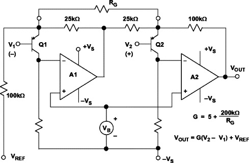
The AD627 in-amp delivers rail-to-rail output swing and operates over a wide supply voltage range (+2.7V to ±18V). Without RG, the external gain-setting resistor, the in-amp gain is 5. Gains up to 1000 can be set with a single external resistor. Common mode rejection of the AD627B at 60 Hz with a 1-kΩ source imbalance is 85 dB when operating on a single +3-V supply and G = 5. Even though the AD627 is a two op-amp in-amp, a patented circuit keeps the CMR flat out to a much higher frequency than would be achievable with a conventional discrete two op-amp in-amp. The AD627 data sheet (available at www.analog.com) has a detailed discussion of allowable input/output voltage ranges as a function of gain and power supply voltages. Key specifications for the AD627 are summarized in Figure 12.51.
Figure 12.51. AD627 in-amp key specifications.
For true balanced high impedance inputs, three op-amps may be connected to form the in-amp shown in Figure 12.52. This circuit is typically referred to as the three op-amp in-amp. The gain of the amplifier is set by the resistor, RG, which may be internal, external, or (software or pin-strap) programmable. In this configuration, CMR depends upon the ratio matching of R3/R2 to R3′/R2′. Furthermore, common mode signals are only amplified by a factor of 1 regardless of gain (no common mode voltage will appear across RG, hence, no common mode current will flow in it because the input terminals of an op-amp will have no significant potential difference between them). Thus, CMR will theoretically increase in direct proportion to gain. Large common mode signals (within the A1-A2 op-amp headroom limits) may be handled at all gains. Finally, because of the symmetry of this configuration, common mode errors in the input amplifiers, if they track, tend to be canceled out by the subtractor output stage. These features explain the popularity of the three op-amp in-amp configuration.
Figure 12.52. Three op-amp instrumentation amplifier.

The classic three op-amp configuration has been used in a number of monolithic IC instrumentation amplifiers. Besides offering excellent matching between the three internal op-amps, thin film laser-trimmed resistors provide excellent ratio matching and gain accuracy at much lower cost than using discrete op-amps and resistor networks. The AD620 is an excellent example of monolithic in-amp technology, and a simplified schematic is shown in Figure 12.53.
Figure 12.53. AD620 in-amp simplified schematic.

The AD620 is a highly popular in-amp and is specified for power supply voltages from ±2.3V to ±18V. Input voltage noise is only 9 nV/√Hz at 1 kHz. Maximum input bias current is only 1 nA maximum because of the Superbeta input stage.
Overvoltage protection is provided by the internal 400-Ω thin-film current-limit resistors in conjunction with the diodes that are connected from the emitter to base of Q1 and Q2. The gain is set with a single external RG resistor. The appropriate internal resistors are trimmed so that standard 1% or 0.1% resistors can be used to set the AD620 gain to popular gain values.
As in the case of the two op-amp in-amp configuration, single-supply operation of the three op-amp in-amp requires an understanding of the internal node voltages. Figure 12.54 shows a generalized diagram of the in-amp operating on a single +5-V supply. The maximum and minimum allowable output voltages of the individual op-amps are designated VOH (maximum high output) and VOL (minimum low output), respectively. Note that the gain from the common mode voltage to the outputs of A1 and A2 is unity, and that the sum of the common mode voltage and the signal voltage at these outputs must fall within the amplifier output voltage range. It is obvious that this configuration cannot handle input common mode voltages of either 0V or +5V because of saturation of A1 and A2. As in the case of the two op-amp in-amp, the output reference is positioned halfway between VOH and VOL in order to allow for bipolar differential input signals.
Figure 12.54. Three op-amp in-amp single +5 V-supply restrictions.
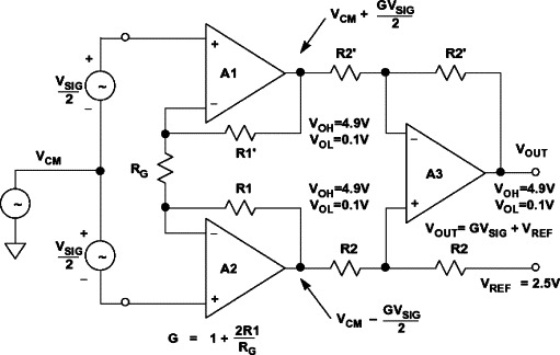
This chapter has emphasized the operation of high-performance linear circuits from a single, low-voltage supply (5V or less) is a common requirement. While there are many precision single-supply operational amplifiers, such as the OP213, the OP291, and the OP284, and some good single-supply instrumentation amplifiers, the highest performance instrumentation amplifiers are still specified for dual-supply operation.
One way to achieve both high precision and single-supply operation takes advantage of the fact that several popular sensors (e.g., strain gauges) provide an output signal centered around the (approximate) midpoint of the supply voltage (or the reference voltage), where the inputs of the signal conditioning amplifier need not operate near “ground” or the positive supply voltage.
Under these conditions, a dual-supply instrumentation amplifier referenced to the supply midpoint followed by a “rail-to-rail” operational amplifier gain stage provides very high DC precision. Figure 12.55 illustrates one such high-performance instrumentation amplifier operating on a single, +5-V supply. This circuit uses an AD620 low-cost precision instrumentation amplifier for the input stage, and an AD822 JFET-input dual rail-to-rail output operational amplifier for the output stage.
Figure 12.55. A precision single-supply composite in-amp with rail-to-rail output.

In this circuit, R3 and R4 form a voltage divider which splits the supply voltage in half to +2.5V, with fine adjustment provided by a trimming potentiometer, P1. This voltage is applied to the input of A1, an AD822 that buffers it and provides a low-impedance source needed to drive the AD620's reference pin. The AD620's reference pin has a 10-kΩ input resistance and an input signal current of up to 200 μA. The other half of the AD822 is connected as a gain-of-3 inverter, so that it can output ±2.5V, “rail-to-rail,” with only ±0.83V required of the AD620. This output voltage level of the AD620 is well within the AD620's capability, thus ensuring high linearity for the “dual-supply” front end. Note that the final output voltage must be measured with respect to the +2.5-V reference and not to GND.
The general gain expression for this composite instrumentation amplifier is the product of the AD620 and the inverting amplifier gains: (12.14)

For this example, an overall gain of 10 is realized with RG = 21.5 kΩ (closest standard value). Figure 12.56 summarizes various RG/gain values and performance.
Figure 12.56. Performance summary of the +5-V single-supply AD620/AD822 composite in-amp.
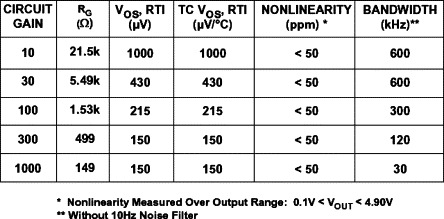
In this application, the allowable input voltage on either input to the AD620 must lie between +2V and +3.5V in order to maintain linearity. For example, at an overall circuit gain of 10, the common mode input voltage range spans 2.25V to 3.25V, allowing room for the ±0.25-V full-scale differential input voltage required to drive the output ±2.5V about VREF.
The inverting configuration was chosen for the output buffer to facilitate system output offset voltage adjustment by summing currents into the A2 stage buffer's feedback summing node. These offset currents can be provided by an external DAC, or from a resistor connected to a reference voltage.
The AD822 rail-to-rail output stage exhibits a very clean transient response (not shown) and a small-signal bandwidth over 100 kHz for gain configurations up to 300. Note that excellent linearity is maintained over 0.1V to 4.9V VOUT. To reduce the effects of unwanted noise pickup, a capacitor is recommended across A2's feedback resistance to limit the circuit bandwidth to the frequencies of interest.
In cases where 0-V inputs are required, the AD623 single-supply in-amp configuration shown in Figure 12.57 offers an attractive solution. The PNP emitter-follower level shifters, Q1/Q2, allow the input signal to go 150 mV below the negative supply and to within 1.5V of the positive supply. The AD623 is fully specified for single-power supplies between +3V and +12V and dual supplies between ±2.5V and ±6V (see Figure 12.58). The AD623 data sheet (available at www.analog.com) contains an excellent discussion of allowable input/output voltage ranges as a function of gain and power supply voltages.
Figure 12.57. AD623 single-supply in-amp architecture.
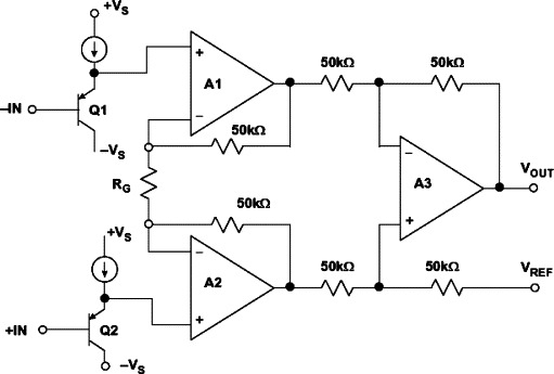
Figure 12.58. AD623 in-amp key specifications.

12.2.5.2. Instrumentation Amplifier DC Error Sources
The DC and noise specifications for instrumentation amplifiers differ slightly from conventional op-amps, so some discussion is required in order to fully understand the error sources.
The gain of an in-amp is usually set by a single resistor. If the resistor is external to the in-amp, its value is either calculated from a formula or chosen from a table on the data sheet, depending on the desired gain.
Absolute value laser wafer trimming allows the user to program gain accurately with this single resistor. The absolute accuracy and temperature coefficient of this resistor directly affects the in-amp gain accuracy and drift. Since the external resistor will never exactly match the internal thin film resistor tempcos, a low-TC (<25 ppm/° C) metal film resistor should be chosen, preferably with a 0.1% or better accuracy.
Often specified as having a gain range of 1 to 1,000, or 1 to 10,000, many in-amps will work at higher gains, but the manufacturer will not guarantee a specific level of performance at these high gains. In practice, as the gain-setting resistor becomes smaller, any errors due to the resistance of the metal runs and bond wires become significant. These errors, along with an increase in noise and drift, may make higher single-stage gains impractical. In addition, input offset voltages can become quite sizable when reflected to output at high gains. For instance, a 0.5-mV input offset voltage becomes 5V at the output for a gain of 10,000. For high gains, the best practice is to use an instrumentation amplifier as a preamplifier then use a postamplifier for further amplification.
In a pin-programmable gain in-amp such as the AD621, the gain-setting resistors are internal, well matched, and the gain accuracy and gain drift specifications include their effects. The AD621 is otherwise generally similar to the externally gain-programmed AD620.
The gain error specification is the maximum deviation from the gain equation. Monolithic in-amps such as the AD624C have very low factory-trimmed gain errors, with its maximum error of 0.02% at G = 1 and 0.25% at G = 500 being typical for this high-quality in-amp. Notice that the gain error increases with increasing gain. Although externally connected gain networks allow the user to set the gain exactly, the temperature coefficients of the external resistors and the temperature differences between individual resistors within the network all contribute to the overall gain error. If the data is eventually digitized and presented to a digital processor, it may be possible to correct for gain errors by measuring a known reference voltage and then multiplying by a constant.
Nonlinearity is defined as the maximum deviation from a straight line on the plot of output versus input. The straight line is drawn between the end points of the actual transfer function. Gain nonlinearity in a high-quality in-amp is usually 0.01% (100 ppm) or less and is relatively insensitive to gain over the recommended gain range.
The total input offset voltage of an in-amp consists of two components (see Figure 12.59). Input offset voltage, VOSI, is that component of input offset which is reflected to the output of the in-amp by the gain G. Output offset voltage, VOSO, is independent of gain. At low gains, output offset voltage is dominant, while at high gains input offset dominates. The output offset voltage drift is normally specified as drift at G = 1 (where input effects are insignificant), while input offset voltage drift is given by a drift specification at a high gain (where output offset effects are negligible). The total output offset error, referred to the input, is equal to VOSI + VOSO/G. In-amp data sheets may specify VOSI and VOSO separately or give the total RTI input offset voltage for different values of gain.
Figure 12.59. In-amp offset voltage model.
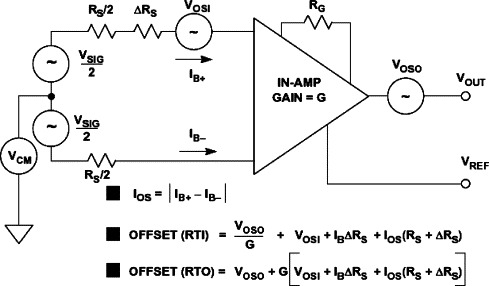
Input bias currents may also produce offset errors in in-amp circuits (see Figure 12.59). If the source resistance, RS, is unbalanced by an amount, ΔRS (often the case in bridge circuits), then there is an additional input offset voltage error due to the bias current, equal to IBΔRS (assuming that IB+ ≈ IB– = IB). This error is reflected to the output, scaled by the gain G. The input offset current, IOS, creates an input offset voltage error across the source resistance, RS + ΔRS, equal to IOS(RS + ΔRS), which is also reflected to the output by the gain, G.
In-amp common mode error is a function of both gain and frequency. Analog Devices specifies in-amp CMR for a 1-kΩ source impedance unbalance at a frequency of 60 Hz. The RTI common mode error is obtained by dividing the common mode voltage, VCM, by the common mode rejection ratio.
Power supply rejection is also a function of gain and frequency. For in-amps, it is customary to specify the sensitivity to each power supply separately. Now that all DC error sources have been accounted for, a worst case DC error budget can be calculated by reflecting all the sources to the in-amp input (Figure 12.60).
Figure 12.60. Instrumentation amplifier DC errors referred to the input.

12.2.5.3. Instrumentation Amplifier Noise Sources
Since in-amps are primarily used to amplify small precision signals, it is important to understand the effects of all the associated noise sources. The in-amp noise model is shown in Figure 12.61. There are two sources of input voltage noise. The first is represented as a noise source, VNI, in series with the input, as in a conventional op-amp circuit. This noise is reflected to the output by the in-amp gain, G. The second noise source is the output noise, VNO, represented as a noise voltage in series with the in-amp output. The output noise, shown here referred to VOUT, can be referred to the input by dividing by the gain, G.
Figure 12.61. In-amp noise model.
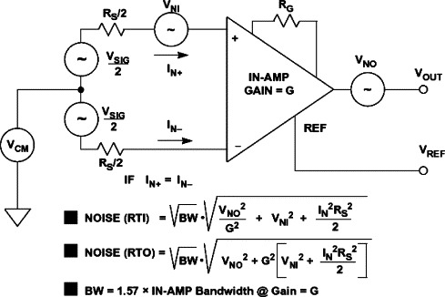
There are two noise sources associated with the input noise currents IN+ and IN–. Even though IN+ and IN– are usually equal (IN+ ≈ IN– = IN), they are uncorrelated, and therefore, the noise they each create must be summed in a root-sum-squares (RSS) fashion. IN+ flows through one half of RS, and IN– the other half. This generates two noise voltages, each having an amplitude, INRS/2. Each of these two noise sources is reflected to the output by the in-amp gain, G.
The total output noise is calculated by combining all four noise sources in an RSS manner: In-amp data sheets often present the total voltage noise RTI as a function of gain. This noise spectral density includes both the input (VNI) and output (VNO) noise contributions. The input current noise spectral density is specified separately. As in the case of op-amps, the total noise RTI must be integrated over the in-amp closed-loop bandwidth to compute the rms value. The bandwidth may be determined from data sheet curves which show frequency response as a function of gain.
12.2.5.4. In-Amp Bridge Amplifier Error Budget Analysis
It is important to understand in-amp error sources in a typical application. Figure 12.62 shows a 350-Ω load cell which has a full-scale output of 100 mV when excited with a 10-V source. The AD620 is configured for a gain of 100 using the external 499-Ω gain-setting resistor. The table shows how each error source contributes to the total unadjusted error of 2145 ppm. The gain, offset, and CMR errors can be removed with a system calibration. The remaining errors—gain nonlinearity and 0.1-Hz to 10-Hz noise—cannot be removed with calibration and limit the system resolution to 42.8 ppm (approximately 14-bit accuracy).
Figure 12.62. AD620B bridge amplifier DC error budget.

12.2.5.5. In-Amp Performance Tables
Figure 12.63 shows a selection of precision in-amps designed primarily for operation on dual supplies. It should be noted that the AD620 is capable of single +5-V supply operation (see Figure 12.55), but neither its input nor its output is capable of rail-to-rail swings.
Figure 12.63. Precision in-amps: data for VS = ±15 V, G = 1000.
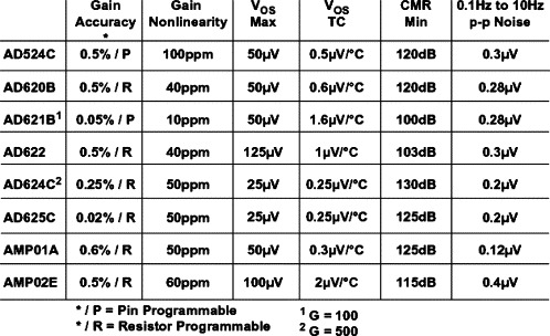
Instrumentation amplifiers specifically designed for single-supply operation are shown in Figure 12.64. It should be noted that, although the specifications in the figure are given for a single +5-V supply, all of the amplifiers are also capable of dual-supply operation and are specified for both dual- and single-supply operation on their data sheets. In addition, the AD623 and AD627 will operate on a single +3-V supply.
Figure 12.64. Single-supply in-amps: data for VS = ±5V, G = 1000.

The AD626 is not a true in-amp but is a differential amplifier with a thin film input attenuator that allows the common mode voltage to exceed the supply voltages. This device is designed primarily for high- and low-side current-sensing applications. It will also operate on a single +3-V supply.
12.2.5.6. In-Amp Input Overvoltage Protection
As interface amplifiers for data acquisition systems, instrumentation amplifiers are often subjected to input overloads, that is, voltage levels in excess of the full scale for the selected gain range (Figure 12.65). The manufacturer's “absolute maximum” input ratings for the device should be closely observed. As with op-amps, many in-amps have absolute maximum input voltage specifications equal to ±VS. External series resistors (for current limiting) and Schottky diode clamps may be used to prevent overload, if necessary. Some instrumentation amplifiers have built-in overload protection circuits in the form of series resistors (thin film) or series-protection FETs. In-amps such as the AMP-02 and the AD524 utilize series-protection FETs, because they act as a low impedance during normal operation and a high impedance during fault conditions.
Figure 12.65. Instrumentation amplifier input overvoltage considerations.
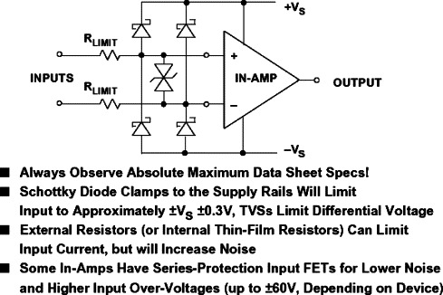
An additional transient voltage suppresser (TVS) may be required across the input pins to limit the maximum differential input voltage. This is especially applicable to three op-amp in-amps operating at high gain with low values of RG.
12.2.6. Chopper-Stabilized Amplifiers
For the lowest offset and drift performance, chopper-stabilized amplifiers may be the only solution. The best bipolar amplifiers offer offset voltages of 10 μV and 0.1 μV/A° C drift. Offset voltages less than 5 μV with practically no measurable offset drift are obtainable with choppers, albeit with some penalties.
The basic chopper amplifier circuit is shown in Figure 12.66. When the switches are in the Z (auto-zero) position, capacitors C2 and C3 are charged to the amplifier input and output offset voltage, respectively. When the switches are in the S (sample) position, VIN is connected to VOUT through the path comprising R1, R2, C2, the amplifier, C3, and R3. The chopping frequency is usually between a few hundred hertz and several kilohertz, and it should be noted that, because this is a sampling system, the input frequency must be much less than one half the chopping frequency in order to prevent errors due to aliasing. The R1/C1 combination serves as an antialiasing filter. It is also assumed that, after a steady-state condition is reached, there is only a minimal amount of charge transferred during the switching cycles. The output capacitor, C4, and the load, RL, must be chosen such that there is minimal VOUT droop during the auto-zero cycle.
Figure 12.66. Classic chopper amplifier.
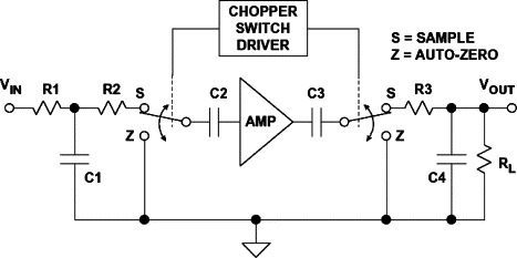
The basic chopper amplifier of Figure 12.66 can pass only very low frequencies because of the input filtering required to prevent aliasing. The chopper-stabilized architecture shown in Figure 12.67 is most often used in chopper amplifier implementations. In this circuit, A1 is the main amplifier, and A2 is the nulling amplifier. In the sample mode (switches in S position), the nulling amplifier, A2, monitors the input offset voltage of A1 and drives its output to zero by applying a suitable correcting voltage at A1's null pin. Note, however, that A2 also has an input offset voltage, so it must correct its own error before attempting to null A1's offset. This is achieved in the auto-zero mode (switches in Z position) by momentarily disconnecting A2 from A1, shorting its inputs together, and coupling its output to its own null pin. During the auto-zero mode, the correction voltage for A1 is momentarily held by C1. Similarly, C2 holds the correction voltage for A2 during the sample mode. In modern IC chopper-stabilized op-amps, the storage capacitors C1 and C2 are on-chip.
Figure 12.67. Chopper-stabilized amplifier.

Note in this architecture that the input signal is always connected to the output through A1. The bandwidth of A1 thus determines the overall signal bandwidth, and the input signal is not limited to less than one half the chopping frequency as in the case of the traditional chopper amplifier architecture. However, the switching action does produce small transients at the chopping frequency which can mix with the input signal frequency and produce in-band distortion.
It is interesting to consider the effects of a chopper amplifier on low-frequency 1/f noise. If the chopping frequency is considerably higher than the 1/f corner frequency of the input noise, the chopper-stabilized amplifier continuously nulls out the 1/f noise on a sample-by-sample basis. Theoretically, a chopper op-amp therefore has no 1/f noise. However, the chopping action produces wideband noise which is generally much worse than that of a precision bipolar op-amp.
Figure 12.68 shows the noise of a precision bipolar amplifier (OP177/AD707) versus that of the AD8551/52/54 chopper-stabilized op-amp. The peak-to-peak noise in various bandwidths is calculated for each in the table below the graphs. Note that, as the frequency is lowered, the chopper amplifier noise continues to drop, while the bipolar amplifier noise approaches a limit determined by the 1/f corner frequency and its white noise (see Figure 12.29). At a very low frequency, the noise performance of the chopper is superior. The AD8551/8552/8554 family of chopper-stabilized op-amps offers rail-to-rail input and output single-supply operation, low offset voltage, and low offset drift. The storage capacitors are internal to the IC, and no external capacitors other than standard decoupling capacitors are required. Key specifications for the devices are given in Figure 12.69. It should be noted that extreme care must be taken when applying these devices to avoid parasitic thermocouple effects in order to fully realize the offset and drift performance.
Figure 12.68. Noise: bipolar vs. chopper amplifier.

Figure 12.69. AD8551/52/54 chopper stabilized rail-to-rail input/output amplifiers.

12.2.7. Isolation Amplifiers
There are many applications where it is desirable, or even essential, for a sensor to have no direct (“galvanic”) electrical connection with the system to which it is supplying data, either in order to avoid the possibility of dangerous voltages or currents from one half of the system doing damage in the other or to break an intractable ground loop (Figure 12.70). Such a system is said to be isolated, and the arrangement that passes a signal without galvanic connections is known as an isolation barrier.
Figure 12.70. Applications for isolation amplifiers.
The protection of an isolation barrier works in both directions and may be needed in either, or even in both. The obvious application is where a sensor may accidentally encounter high voltages and the system it is driving must be protected. Or a sensor may need to be isolated from accidental high voltages arising downstream, in order to protect its environment: Examples include the need to prevent the ignition of explosive gases by sparks at sensors and the protection from electric shock of patients whose ECG, EEG, or EMG is being monitored. The ECG case is interesting, as protection may be required in both directions: The patient must be protected from accidental electric shock, but if the patient's heart should stop, the ECG machine must be protected from the very high voltages (>7.5 kV) applied to the patient by the defibrillator that will be used to attempt to restart it.
Just as interference, or unwanted information, may be coupled by electric or magnetic fields, or by electromagnetic radiation, these phenomena may be used for the transmission of wanted information in the design of isolated systems. The most common isolation amplifiers use transformers, which exploit magnetic fields, and another common type uses small high-voltage capacitors, exploiting electric fields. Opto-isolators, which consist of an LED and a photocell, provide isolation by using light, a form of electromagnetic radiation. Different isolators have differing performance: Some are sufficiently linear to pass high-accuracy analog signals across an isolation barrier, with others the signal may need to be converted to digital form before transmission, if accuracy is to be maintained, a common application for V/F converters.
Transformers are capable of analog accuracy of 12–16 bits and bandwidths up to several hundred kilohertz, but their maximum voltage rating rarely exceeds 10 kV and is often much lower. Capacitively coupled isolation amplifiers have lower accuracy, perhaps 12-bits maximum, lower bandwidth, and lower voltage ratings—but they are cheap. Optical isolators are fast and cheap and can be made with very high-voltage ratings (4–7 kV is one of the more common ratings), but they have poor analog domain linearity and are not usually suitable for direct coupling of precision analog signals.
Linearity and isolation voltage are not the only issues to be considered in the choice of isolation systems. Power is essential. Both the input and the output circuitry must be powered, and unless there is a battery on the isolated side of the isolation barrier (which is possible but rarely convenient), some form of isolated power must be provided. Systems using transformer isolation can easily use a transformer (either the signal transformer or another one) to provide isolated power, but it is impractical to transmit useful amounts of power by capacitive or optical means. Systems using these forms of isolation must make other arrangements to obtain isolated power supplies—this is a powerful consideration in favor of choosing transformer-isolated isolation amplifiers: They almost invariably include an isolated power supply.
The isolation amplifier has an input circuit that is galvanically isolated from the power supply and the output circuit. In addition, there is minimal capacitance between the input and the rest of the device. Therefore, there is no possibility for DC current flow, and minimum AC coupling. Isolation amplifiers are intended for applications requiring safe, accurate measurement of low-frequency voltage or current (up to about 100 kHz) in the presence of high common mode voltage (to thousands of volts) with high common mode rejection. They are also useful for line-receiving of signals transmitted at high impedance in noisy environments, and for safety in general-purpose measurements, where DC and line-frequency leakage must be maintained at levels well below certain mandated minimums. Principal applications are in electrical environments of the kind associated with medical equipment, conventional and nuclear power plants, automatic test equipment, and industrial process control systems.
In the basic two-port form, the output and power circuits are not isolated from one another. In the three-port isolator shown in Figure 12.71, the input circuits, output circuits, and power source are all isolated from one another. The figure shows the circuit architecture of a self-contained isolator, the AD210. An isolator of this type requires power from a two-terminal DC power supply. An internal oscillator (50 kHz) converts the DC power to AC, which is transformer-coupled to the shielded input section, then converted to DC for the input stage and the auxiliary power output. The AC carrier is also modulated by the amplifier output, transformer-coupled to the output stage, demodulated by a phase-sensitive demodulator (using the carrier as the reference), filtered, and buffered using isolated DC power derived from the carrier. The AD210 allows the user to select gains from 1 to 100 using an external resistor. Bandwidth is 20 kHz, and voltage isolation is 2500V rms (continuous) and ±3500V peak (continuous).
Figure 12.71. AD210 three-port isolation amplifier.

The AD210 is a three-port isolation amplifier: The power circuitry is isolated from both the input and the output stages and may therefore be connected to either—or to neither. It uses transformer isolation to achieve 3500-V isolation with 12-bit accuracy. Key specifications for the AD210 are summarized in Figure 12.72.
Figure 12.72. AD210 isolation amplifier key features.

A typical isolation amplifier application using the AD210 is shown in Figure 12.73. The AD210 is used with an AD620 instrumentation amplifier in a current-sensing system for motor control. The input of the AD210, being isolated, can be connected to a 110- or 230-V power line without any protection, and the isolated ±15V power the AD620, which senses the voltage drop in a small current sensing resistor. The 110- or 230-V rms common mode voltage is ignored by the isolated system. The AD620 is used to improve system accuracy: The VOS of the AD210 is 15 mV, while the AD620 has VOS of 30 μV and correspondingly lower drift. If higher DC offset and drift are acceptable, the AD620 may be omitted, and the AD210 used directly at a closed loop gain of 100.
Figure 12.73. Motor control current sensing.
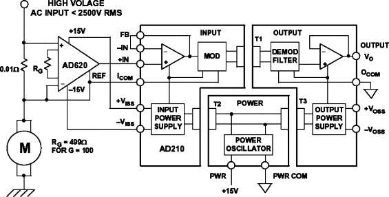
References
1 Ramon Pallas-Areny, John G. Webster, Sensors and Signal Conditioning 1991 John Wiley New York
2 Dan Sheingold, Transducer Interfacing Handbook 1980 Analog Devices, Inc.
3 Walt Kester, Amplifier Applications Guide 1992 Analog Devices, Inc. sections 2, 3
4 Walt Kester, System Applications Guide 1993 Analog Devices, Inc. sections 1, 6
5 AD7730 Data Sheet, Analog Devices, available at www.analog.com.
1 Walt Jung, Op Amp Applications Handbook 2005 Newnes Boston
2 Amplifier Applications Guide 1992 Analog Devices, Inc.
3 System Applications Guide 1994 Analog Devices, Inc.
4 Linear Design Seminar 1995 Analog Devices, Inc.
5 Practical Analog Design Techniques 1995 Analog Devices, Inc.
6 High Speed Design Techniques 1996 Analog Devices, Inc.
7 James L. Melsa, G. Donald, Linear Control Systems 1969 McGraw-Hill New York196-220
8 Thomas M. Fredrickson, Intuitive Operational Amplifiers 1988 McGraw-Hill New York
9 Paul R. Gray, Robert G. Meyer, Analysis and Design of Analog Integrated Circuits 2nd edition 1984 John Wiley New York
10 J.K. Roberge, Operational Amplifiers-Theory and Practice 1975 John Wiley New York
11 Lewis Smith, Dan Sheingold, Noise and operational amplifier circuits Analog Dialogue 25th Anniversary Issue 199119-31 (Also AN358)
12 D. out, M. Kaufman, Handbook of Operational Amplifier Circuit Design 1976 McGraw-Hill New York
13 Joe Buxton, Careful design tames high-speed op amps Electronic Design 1991 (April 11)
14 J. Dostal, Operational Amplifiers 1981 Elsevier Scientific Publishing New York
15 Sergio Franco, Design with Operational Amplifiers and Analog Integrated Circuits 2nd edition 1998 McGraw-Hill New York
16 Charles Kitchin, Lew Counts, Instrumentation Amplifier Application Guide 1991 Analog Devices
17 AD623 and AD627 Instrumentation Amplifier Data Sheets, Analog Devices, available at www.analog.com
18 Eamon Nash, A practical review of common mode and instrumentation amplifiers Sensors Magazine 199826-33 July
19 Nash, Eamon. Errors and Error Budget Analysis in Instrumentation Amplifiers. Application Note AN-539. Analog Devices.