
Chapter 20. Inspection Test
Living with ever-increasing component complexity and board density, along with decreased nodal access, test engineers must face the reduced efficiency of traditional test strategies. Yet the need to ship good products has become more critical than ever. Customers expect that their electronic products will work the first time without difficulty, and that they will continue to work with a minimum of fuss.
To cope, manufacturers are turning to inspection as complement or supplement to traditional test. Inspection, when it works, offers numerous advantages over test. It requires neither bed-of-nails nor edge-connector fixtures. Good-board criteria against which you compare the board under test may come from a known-good board (or a number of them to establish appropriate tolerances) or from a simulation. Also, most inspection is noninvasive. That is, it does not exercise or otherwise disturb the circuit.
On the other hand, inspection can determine that the board looks correct, but it cannot verify that the board works. Only a true test can establish functionality. Test and inspection represent a trade-off, as Figure 20.1 illustrates. Taking maximum advantage of inspection can simplify requirements for subsequent test, which leads to a recommendation that I hope will become an industry mantra: “Inspect everything you can, test only what you must.”
Figure 20.1. Test and inspection represent a trade-off. Extra effort expended at the inspection stage should reduce the test burden downstream.

The inspection equivalent of a test program consists primarily of a representation of a good board's physical-layout specifications and a collection of rules and heuristics to decide whether the board under scrutiny conforms sufficiently. Perhaps the greatest caveat that accompanies most inspection techniques is that unless the heuristics allow for sufficient variation in judging what constitutes a good board, the step will produce excessive numbers of false failures.
Test, on the other hand, relies on input signals and output measurements, which, at least to some degree, require exercising the circuit to determine its quality. An improperly designed test on a board containing a catastrophic fault can aggravate existing problems. Powering up a board containing a short, for example, accomplishes little beyond frying working circuitry and verifying the performance of the facility's smoke detectors.
Creating inspection algorithms generally takes much less time than developing comparable test programs does. Also, most manufacturers place inspection before test in the process. As a result, finding and repairing faults during inspection generally costs considerably less than uncovering and correcting those same problems during test. In addition, inspection can find faults that defy electrical test. Insufficient solder, mouse bites on traces, and other problems do not show up during test because they do not directly affect board performance—yet. Sometimes a solder joint may appear to make adequate contact even if it contains no solder at all. These problems increase the likelihood that a previously functioning board will fail in the field, after it has been shaken during shipping, for example. Repairing boards before they leave the factory improves product reliability. Therefore, if you can economically justify both inspection and test steps, shift as much as possible of the fault-finding burden to inspection.
At the same time, inspection cannot uncover many problems that show up routinely during test. Inspection's ability to detect an incorrect part is extremely limited. Test, however, can find exactly those problems. In-circuit and other bed-of-nails techniques measure single components or clusters to determine if they are correct and function properly. Functional, emulation, or system test examines the behavior of the board (or system) as a whole.
20.1. Striking a Balance
Neither test nor inspection can find all faults for all manufacturing lines. Certainly coverage overlaps, which can lead to the mistaken impression that one technique or the other will suffice. But the areas of overlap are not sufficient. Each approach has strengths and weaknesses that engineers must consider when deciding on the best strategy.
Unfortunately for test engineers, inspection often falls into the “not invented here” category, because in many organizations inspection comes under the purview of the manufacturing rather than the test department. Any attempt to replace portions of the test strategy with inspection steps is often perceived as a threat to job security. This attitude emphasizes the necessity of encouraging the “we're all in this together” philosophy. Buckminster Fuller, engineer and Renaissance thinker, contended that the solution to the problem of trade imbalances around the world was to simply draw a line around the planet and call it one market. This eliminates the problem of “them vs. us” because “them is us,” so there is no imbalance. The same philosophy applies to manufacturing and test responsibilities. All quality steps, including process monitoring and feedback, inspection, test, and repair belong to the same basic task—getting only good products out the door. If “them is us,” then including inspection in what would otherwise be “merely” a test strategy creates no imbalance in responsibility—only a shift in timing. And because inspection usually precedes test, finding and dealing with problems during inspection costs less than doing so later.
Lack of access to board nodes often drastically reduces the effectiveness of bed-of-nails test techniques. Shifting the burden to functional and system test usually means increasing the time required for test-program development, debugging, and implementation. Once again, pressures to shorten time to market strain the ability to adopt this approach.
Ironically, many common factors both encourage and discourage including inspection as part of an overall “test” strategy, as Figure 20.2 shows. Smaller parts and denser board placement make bed-of-nails access more difficult, but they also complicate the lives of human visual inspectors and require higher-resolution inspection equipment. The need for higher resolution, in turn, increases camera-positioning time and image-processing time, which slows the inspection step and increases the likelihood that lighting or other conditions during inspection will falsely flag good boards as bad. More complex components mean analyzing more solder joints placed closer together. Increasing use of BGAs, flip chips, and other hidden-node device designs precludes human and automated optical inspection, because those techniques cannot see nodes out of the line of sight. The increased use of complex, low-volume boards in today's products favors inspection because of its shorter program-development time as compared with conventional test. These same boards require fast ramp-up to full production, making it unlikely that engineers will have time to fine-tune the inspection equipment to more easily differentiate between marginally good and marginally bad boards.
Figure 20.2. These factors both encourage and discourage inspection as part of a “test” strategy.
An effective inspection step can verify both a product's quality and reliability. As mentioned earlier, quality denotes that a product performs to specification. Reliability indicates the degree to which the product will continue to perform to specification—and without failure—during actual use. Test, in contrast to inspection, concentrates primarily on quality issues.
Historically, “inspection” evoked images of armies of human beings examining tiny board features looking for problems. In fact, human visual inspection (HVI) remains a huge part of the industry's inspection arsenal. A few years ago, Stan Runyon at Electronic Engineering Times speculated that 40,000 human beings still performed this function, despite its declining effectiveness in the face of advances in board technology.
In fact, inspection covers much more ground than the human beings armed with magnifying glasses or microscopes looking for anomalies on the board surface. Figure 20.3 shows the various stages of the manufacturing process, and the test or inspection requirements at each stage. Figure 20.4 shows the types of test and inspection that can serve those needs.
Figure 20.3. The various stages of the manufacturing process and the test or inspection requirements at each stage (Teradyne).

Figure 20.4. The types of test and inspection that can serve the needs depicted in Figure 20.3 (Teradyne).

As you can see, inspection can take place at any or all of three process locations. Postpaste inspection examines the board after the paste printer has deposited solder, before assembly operations have added components. Postplacement inspection occurs after pick-and-place machines, chip shooters, and human assemblers have finished their tasks. Postreflow (it could also be called post-wave-solder, but most soldering these days avoids that error-prone step) takes place after boards have emerged from reflow ovens, when the final solder joints are available for qualitative and quantitative analysis.
20.2. Postpaste Inspection
Examining the board immediately after paste deposition enjoys numerous advantages. Inspection at this stage looks for a number of fault types. A clogged aperture in the printer stencil, for example, can prevent solder from reaching some pads, or the solder deposited may be insufficient to create an acceptable joint later on. This step can also find residual solder where it does not belong on the board. Measuring the area of solder on the pad permits a reasonable estimate of the quantity of solder deposited, a reasonable predictor of final solder-joint integrity. Off-pad solder, like that on the board in Figure 20.5, can also cause device-connection problems later on.
Figure 20.5. Inspecting immediately after solder-paste printing will find problems such as off-pad solder

(Photo courtesy Teradyne).
One of the primary benefits of postpaste inspection is the ease and low cost of board repair. Fixing the board at this stage requires merely washing the solder from the board and returning it to the “back of the line” in the manufacturing process, ready for another go. This step eliminates many problems before they escape to downstream test processes. Some manufacturers estimate that up to 80% of manufacturing faults on surface-mount boards result from problems at the solder-paste step.
Postpaste inspection can take several forms. Some companies still use human inspectors, but the number and size of solder pads and the difficulty of conclusively determining solder-pad registration limits their effectiveness.
The least expensive equipment-supported technique takes advantage of the capabilities of the paste printer itself. Paste printers include their own cameras to detect fiducials on the boards, as well as to facilitate process setup and calibration. These cameras can double as inspectors. They can look down at the board to detect solder anomalies and look up to find clogged apertures and other irregularities in the stencils. This technique is inexpensive and effective within limits (and subject to the ever-present trade-off between cycle time and inspection resolution). However, it provides only two-dimensional images, limiting the accuracy of solder-volume calculations and, therefore, joint-quality predictions. On the other hand, some manufacturers contend that the area of solder alone correlates well with volume, even without height measurements.
The printer camera cannot look for fiducials and examine solder pads at the same time. The printer deposits the solder, then the camera inspects the results. In high-volume operations, the time required for this two-cycle process generally proves prohibitive. On the other hand, manufacturing engineers in low-volume environments need not concern themselves with the time constraint.
To cope with throughput limitations, some companies use the camera to examine only certain board areas that they consider either typical or critical. Also, some engineers use the camera during paste-print setup to ensure correct stencil loading and positioning, paste-pressure adjustment, and proper paste dispensing. They inspect the first few boards and make any necessary process modifications, then turn off the camera to avoid slowing the process during routine production.
In addition to solder-paste area and position, three-dimensional inline techniques profile solder height to precisely calculate its volume. Proponents contend that irregularities in the shape of the solder on the board make solder-volume calculations from only pad-area coverage inaccurate. Some three-dimensional systems inspect the entire surface of every board through the process. Slower and less-expensive systems examine critical board areas or production samples.
The more common approach to three-dimensional postpaste inspection scans a laser across each solder pad, starting with a line across the pad edge and moving perpendicularly until the laser has covered the entire pad. The equipment then measures solder height by a technique called reflective interference, from which it calculates the volume. Some such systems create a complete volume map of solder paste. To attain adequate speeds for full production, other systems may calculate volume by measuring height from line-scans at one or a few locations.
Another approach projects a diffraction fringe pattern on the board, then calculates height and volume by examining the pattern with a stroboscopic white light. This variation avoids the need to scan the board, thereby increasing inspection speeds. Supporters of this variation contend that it provides as much and as accurate information about the solder joint as the laser scan in less time.
Programming for three-dimensional inspection in-line begins with sites that will accommodate fine-pitch components, BGAs, flip chips, and other chip-scale packages. If time permits, the step can look for clogged stencil apertures and similar problems.
Manufacturers can use this type of inspection as a “real-time alarm”—stopping the line if measurements exceed established tolerances—or merely record the information and move on.
The primary limitation in all three-dimensional inspection techniques is that obtaining a useful reflection for analysis depends on the angle of incidence between the light source and the board under test. Irregularities or reflection variations in the board surface, as well as the reflectivity of the solder itself may affect results. The inspection step must also locate the board surface to determine how much of the measured height is solder. Examining both sides of a double-sided board requires two separate inspections.
20.3. Postplacement/Postreflow
Once components have been assembled onto the board, inspection looks for a number of additional manufacturing conditions: the presence or absence of components, component height, some incorrect components (if the incorrect part is significantly different in size or appearance), as well as the accuracy of pick-and-place machines and chip shooters.
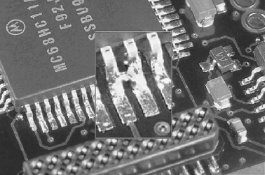
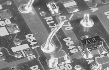
After the reflow oven, inspection performs a final check of solder-joint geometry, solder-joint integrity, and any component movement while the board is in the oven. Realizing that few manufacturers inspect both pre- and postreflow, this step also looks for component existence and position, component identification (subject to the same caveat as earlier), trace existence, and trace defects such as “mouse bites.” Figures 20.6 through 20.11 show some common failure types.
Figure 20.6. These two photographs show boards containing missing-component faults
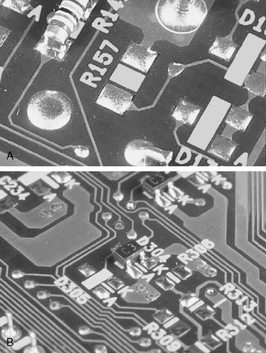
(Photos courtesy Teradyne).
Figure 20.7. A solder short
(Photo courtesy Teradyne).
Figure 20.8. Tombstoning

(Photo courtesy Teradyne).
Figure 20.9. A lifted component leg

(Photo courtesy Teradyne).
Figure 20.10. An off-registration or off-pad component

(Photo courtesy Teradyne).
Figure 20.11. Untrimmed leads of a through-hole component
(Photo courtesy Teradyne).
Some manufacturers use laser or white-light techniques to examine loaded boards. This approach constructs a three-dimensional profile of the board, detecting missing and some off-pad components. The technique is generally too slow for this process stage, however, and one of the others will likely produce more accurate results. Nevertheless, for a cursory check of certain critical board areas, it may be sufficient.
20.3.1. Manual Inspection
As mentioned earlier, despite the preponderance of incredible shrinking electronics, the most common inspection technique remains manual inspection, also known as human visual inspection and manual visual inspection (MVI). Its popularity persists despite a consistent body of evidence that it is less effective than it used to be, always assuming that it was ever effective at all.
Manual inspection consists of a cadre of people examining boards either with the naked eye or aided by magnifying glasses or microscopes. Manufacturers like the technique because it is relatively simple and inexpensive to deploy. Microscopes and magnifying glasses require little up-front investment, and people costs are easy to manage and adjust as situations change. Its flexibility stems from the fact that human beings adapt much more easily to new situations than machines do. Also, manual inspectors are much less bothered by changes in lighting or other environmental conditions. There is no need for programming, and, within the limits of the inspectors' capability, it can be quite accurate.
On the other hand, operating costs are quite high. Labor costs represent a considerable expense, and adjusting the workforce as manufacturing throughput changes is awkward at best. Success of HVI depends a great deal on the experience and diligence of the inspectors. Difficult boards or subtle problems can slow the process and reduce the technique's accuracy and effectiveness. Also, whereas machines make a “yes/no” decision based on established specifications and heuristics, people's judgments are often more subjective. As a result, the consistency of manual inspection leaves much to be desired. According to one study from AT&T, now more than a decade old, two inspectors examining the same boards under the same conditions agreed only 28%of the time. With three inspectors, agreement dropped to 12%, and with four inspectors, to 6%. Even the same inspector examining a board twice came up with an identical diagnosis only 44% of the time. With today's smaller feature sizes, the situation would likely be worse. In many (if not most) cases, one of the automated techniques would work considerably better.
Human inspection also suffers from inconsistency based on the time of day or the day of the week—the previously mentioned “Monday/Friday syndrome,” named after an admonition by Ralph Nader in the 1970s never to buy a car manufactured on Monday morning or Friday afternoon. Manual inspectors often miss failures, while flagging and unnecessarily touching up good joints.
The last drawback to this technique applies to all the visual methods, as well as to laser and white-light approaches when manufacturers use them on loaded boards. They require line-of-sight access to the features they are inspecting. Since one of the reasons for turning to inspection instead of conventional bed-of-nails test is lack of access, the implications of this limitation are significant.
20.3.2. Automated Optical Inspection
Automated optical inspection (AOI) consists of a camera or other image input and analysis software to make the pass/fail decision. Implementations include the following range of applications:
- A spot check of critical board areas
- A cursory check for component existence and orientation
- Comprehensive analysis of the entire board surface
AOI systems use several techniques to identify failures. Template matching compares the image obtained from a theoretical “golden” image (assuming one is available either from a good board or a CAD simulation). Template matching is somewhat unforgiving of deviations from perceived good-board specifications and of ECOs and other board modifications. The latter remain very common during the early stages of production ramp-up. Pattern matching stores examples of both good and bad boards, comparing the board under test to these standards. Statistical pattern matching works similarly, except that the pattern represents a compendium of a number of boards, so minor deviations will less likely cause false failures. In fact, its proponents contend that statistical pattern matching can produce orders-of-magnitude fewer false calls than its simpler siblings do.
Humans perform better than machines on recognizing image patterns. Nevertheless, even when features are large enough to be detected by human inspectors, machines succeed better on the monotonous task of inspecting identical products. Machines are faster, and inspection times do not vary from one board to the next. It takes fewer workers to run automated equipment than to inspect boards manually, and automation requires less-skilled (and therefore less-expensive) workers. Therefore, adopting AOI generally lowers labor costs. Also, automated systems can resolve finer features than human beings can, although manufacturers have to trade off resolution against throughput. The finer the required resolution, the longer it takes to inspect a board.
AOI enjoys other advantages over manual inspection. By reducing the number of false failures, it reduces costs and improves the productivity of rework operations. Consistency of results allows feeding information back into the process to prevent future failures, improving quality out of manufacturing and consequently lowering test and repair burdens as the product matures.
When compared to conventional test, AOI can more easily reside in an automated production line with a minimum of human intervention. Because it can detect many faults that otherwise rely on electrical tests, manufacturers can sometimes eliminate the process-test step altogether, reducing capital-investment costs by avoiding a test-equipment purchase or freeing an existing tester for other product lines. AOI provides data that test cannot on parts-placement accuracy, which can affect future product quality. Also, positioning AOI after parts placement and before reflow (and therefore before the possibility of electrical test) can avoid extra reflow steps and thereby lower repair and rework costs.
Of course, as a wise soul once said, “No good deed ever goes unpunished.” AOI obviously requires a significantly larger capital investment than does manual inspection. Equipment often costs hundreds of thousands of dollars, including conveyors and other related infrastructure enhancements. Therefore, overall startup costs are higher. The equipment requires “programming” in some form, whereas human inspectors can generally work from existing documentation. For the same reason, implementing engineering changes and product enhancements takes longer and incurs more costs in the automated case.
Humans can make pass/fail decisions even when devices are partially hidden. (A characteristic of humans that machines have thus far failed to match is our ability to draw conclusions from incomplete information. The binary nature of machine logic makes such “fuzzy” decision-making complicated at best.) Human inspectors can also more easily allow for color, size, and other cosmetic variations in the board's parts, as well as lighting variations and other less-than-optimal conditions.
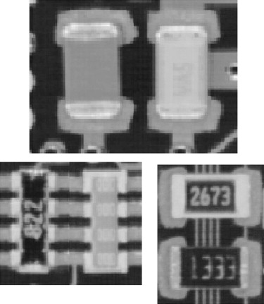
AOI looks for very specific features—part placement, part size, perhaps board fiducials of a certain size and position, and patterns of light and dark, such as bar codes. It can also look at label type fonts and sizes, although this level of resolution slows the inspection step. Unfortunately, many boards include components that exhibit large variations in package sizes and styles. Figure 20.12 shows several examples of electrically identical components that appear different to an AOI system. Automated inspection must also deal with changes in background color and reflectivity and differences in silk-screen typefaces and sizes on allegedly identical boards.
Figure 20.12. Many electrically identical components appear different to an AOI system (GenRad).
AOI suffers disadvantages when compared to conventional test as well. Inspection times are generally longer because of the time required for x-y positioning and image evaluation. AOI cannot find numerous fault types that test can find easily, and many users report a significant increase in false failures. Unlike conventional test, an AOI system requires that the areas under scrutiny be visible by line of sight, and a board containing components on both sides requires two inspection steps. (Instead of inspecting the same board twice, some manufacturers pass the board between two AOI systems, thereby examining both board sides at the same time.) Constructing a reasonably accurate inspection “program” requires a good board or good-board simulation, not always easy during the often fast-changing period of final preparation for production.
Some companies are turning to AOI systems to examine ball-grid arrays (BGAs) before placing them on boards. This inspection step confirms the existence and position of the solder balls, as well as their diameter. Insufficient solder in the balls will likely pass an electrical test after reflow, yet may pose a reliability problem for customers. Even tested BGAs can lose solder balls or experience other problems during handling. Other analysis techniques used after board assembly (such as X-ray) can be expensive or impractical for detecting this situation. Adopting this step can reduce the number of scrapped boards and devices, thereby lowering manufacturing costs.
BGA inspection can also look for excess solder-ball oxidation by gray-level analysis. This condition usually manifests on whole lots of BGAs, rather than on individual components, so identifying it permits repair or returning parts to vendors. Although excess oxidation has never proven to represent a real defect, most manufacturers will reject such BGAs, anticipating possible poor bump bonds and possible poor wetting during underfill. Identifying this situation on BGAs before assembly allows correction at much lower cost than scrapping BGAs or whole boards later.
20.3.3. Design for Inspection
The success of an AOI step depends on the ease with which the camera can distinguish the features that it inspects and the degree to which the board under test conforms to the good-board standard. Several simple steps can make inspection more efficient and more successful.
Maintain consistent size specifications for particular components. For example, 603 discrete component specifications list a size of 60 × 30 mils. Actual devices, however, can vary from 50 × 22 mils to 65 × 34 mils, depending on vendor. If you permit such a wide variation, an AOI system cannot determine whether a device on the board is correct. Therefore, select a single component vendor or a group of vendors who provide visually similar products.
Place components on the board with consistent orientation. This step will make inspection-system programming easier and will facilitate repair and rework operations later. For the same reasons, it is preferable to select parts with the same pin-1 designator (cut corner, colored dot, stripe, dimple).
Some manufacturers advocate specific techniques to facilitate determining the component's exact position on the board. Placing fiducials on the component, as in Figure 20.13, or painting the component site with a contrasting color, as in Figure 20.14, makes position measurements more precise and reduces the number of false failures. Fiducials on the component site, as in Figure 20.15, help the AOI system make a presence/absence decision.
Figure 20.13. Fiducials on the component permit more precise determination of its position (GenRad).

Figure 20.14. Painting the component site in a contrasting color allows the AOI system to more easily detect the component edge (GenRad).

Figure 20.15. The component will cover fiducials on the site, enhancing presence/absence detection capability (GenRad).

AOI is becoming increasingly common, experiencing a year-on-year growth rate exceeding 20%. Current trends in board technology leave manufacturers with few viable alternatives. Higher speeds, better spatial resolution, and more accurate fault detection also combine to increase its effectiveness and therefore its popularity.
20.3.4. Infrared Inspection—A New Look at an Old Alternative
Many kinds of board faults exhibit a higher inherent resistance than their faultless counterparts do. When powered, however briefly, these areas heat up, becoming detectable by infrared inspection. In the same way, infrared techniques can also reveal marginal components, traces, and solder joints that often surface as early field failures.
Infrared inspection is not new. For years, manufacturers have used the technique to examine bare boards for hairline shorts, inner-layer shorts, and similar defects by applying power to the board and looking for “hot spots.” Spatial resolution hovered in the range of 50 μ and reliable defect detection required temperature changes greater than about 1.5° C. In addition, since testing generally took place in the open air, the method had to endure an inconsistent and unpredictable thermal environment combined with the indigenous random noise inherent in infrared camera images. However attractive the theory, these limitations precluded attempts to apply the approach to loaded boards.
20.3.4.1. A New Solution
At least one manufacturer is addressing these concerns, introducing a controlled-environment infrared-inspection station that detects temperature differences as low as 0.025° C on features as small as 5 μ × 5 μ. Its proponents claim that in benchmarks and field trials, the system has detected most of the fault types of X-ray techniques, as well as cracked solder joints and other potential reliability problems that no other approach can find directly, at much lower cost than X-ray equipment.
The new solution tests the board in a controlled isothermal chamber, applying power and input patterns and comparing the infrared signature with a standard assembled from a set of known-good boards. Deviations from the standard generally show up as hot or cold spots whose temperature lies outside the three-standard-deviations limits of the normal statistical error function.
One immediate advantage to this technique is that node visibility—either by line of sight for visual inspection or access through a bed of nails—becomes irrelevant. The tester hooks up to the board via the edge connector, just as in a traditional functional test. Input patterns can be adopted directly from design simulations to exercise the board and ensure that it works properly. Most companies create such patterns during product development. The manufacturer need not generate fault simulations or conventional test programs, saving a significant amount of work and time.
Many fault classes lend themselves to this type of detection. It can find solder voids, misaligned or missing components, insufficient solder, shorts, and broken connections with few false failures. Infrared inspection cannot identify joints with excess solder, which most manufacturers regard as process faults and which X-ray techniques will find, because the circuit appears to function normally.
Infrared also detects failures that X-ray misses. A cold solder joint, a faulty ASIC, or an incorrect resistor, for example, could significantly change the board's thermal signature, but would look no different in an X-ray image. In that respect, the infrared technique resembles a functional test more than it does other forms of inspection. The technique's supporters suggest placing it in the process after in-circuit or other bed-of-nails test, possibly in place of functional test. This configuration avoids adding a step that would lengthen the manufacturing process, introduce another cycle of board handling, and possibly increase solder-joint breakage and other handling-related failures.
20.3.4.2. Predicting Future Failures
Perhaps the most interesting aspect of the infrared approach is its ability to detect latent defects—defects that do not affect the board's current performance but which may represent reliability problems after the product reaches customers. Since the components still function and the board as a whole still works, these faults generally defy conventional detection. Cracked solder joints, for example, force the board current through a smaller-than-normal connection, creating a hot spot that this tester will see. Some marginal components also fall into this fault category.
To find such faults, manufacturers traditionally subject their boards to some form of environmental stress screening (ESS), including burn-in, temperature cycling, and vibration, before performing an in-circuit or functional test. The idea is to aggravate the latent faults until they become real faults and therefore visible to subsequent test. Aside from requiring higher costs for equipment, factory floor space, extra people, longer production times, and larger inventories, ESS stresses good and bad components alike. Some authorities suspect that such screening reduces overall board reliability and shortens board life. In addition, vibration—the second most effective screen after temperature cycling—is difficult to control and cannot apply stresses evenly across the board, so results can be inconsistent.
In contrast, stimulation during an infrared test subjects boards to no more stress than they would experience in normal use. In one field test conducted by an automotive manufacturer, the infrared test found all known failures from a sample group of defective boards, whereas various versions of ESS revealed no more than 42%. In addition, the infrared system discovered that 2% of the boards contained failures of which the manufacturer was unaware.
20.3.4.3. The Infrared Test Process
To build the good-board model, a test engineer views a computer image of the board, highlights each component and area of interest with the computer's mouse, identifies the component, and enters other pertinent data. From this information and a user-supplied input pattern that mimics the board's actual operation, the system assembles a database.
Next, an operator feeds production boards to the system, positioning each board's tooling holes on matching tooling pins in the isothermal chamber. The tooling pins and I/O connectors represent the only “fixture” that the method requires. Each board generates a set of infrared images when executing the test pattern. A statistical analysis of the resulting signatures produces the standard against which the system will measure each board during testing. The tester will flag any uncovered outliers in the sample as bad boards and does not include them in the standard.
The production test itself is relatively straightforward. An operator puts a board into the isothermal chamber, positions it on the tooling pins, and connects the edge connector and any other connectors. After reading the ambient infrared image, the tester powers up the board very briefly (to prevent any shorts from frying it) and again examines its thermal signature. Image-analysis software compares this result to the good-board signature and makes a go/no-go decision. Shorts (including power-to-ground shorts, which are nearly undetectable by conventional test) show up as statistically significant temperature differences at particular board locations, as in Figure 20.16. A failing board at this stage would proceed to repair before continuing, as with both in-circuit and functional test.
Figure 20.16. Infrared inspection shows “hot spots” or “cold spots” when the board under test differs from the good-board standard

(ART Advanced Research Technologies, St. Laurent, Quebec, Canada).
Once the board is short-free, the tester applies power and an input/output stimulation pattern. Testing a cellular phone board, for example, would verify dialing, “press to talk,” and other features. Again, any faults should exhibit obvious differences from the good-board thermal signature.
20.3.4.4. No Good Deed
Like other techniques, infrared inspection has its drawbacks. Chief among them is the need for up to 30 production boards from which the system assembles the good-board signature. Many manufacturers never see that many good boards until after production begins, by which time the test must already be in place. Regardless of the cost benefit of anomaly detection, a manufacturer may encounter the “chicken-and-egg” problem—needing a test to generate 30 good boards and needing the 30 good boards to create the test. In high-mix, low-volume, and low-cost situations this requirement could prove prohibitive.
An out-of-tolerance resistor or capacitor will not generally produce a thermal signature sufficiently different from a good one to be detectable. Such failures are relatively rare, however, and an in-circuit test will usually identify them prior to infrared inspection.
An infrared detector cannot see through certain barriers, such as RF shields and heat sinks. Such boards would require testing before attaching these parts, which may be impractical, and will certainly miss any faults induced during attachment.
Infrared inspection can identify the component containing a failure, but its resolution is not always sufficient to identify the exact pin location, especially for solder problems on small-pitch surface-mount boards. In addition, the thermal anomaly might not occur exactly at the fault. However, a repair technician can call up the failing thermal image on a computer monitor to examine it before proceeding. The anomaly's location narrows the search for the actual fault to a few pins. With that information, the technician can pinpoint the actual problem.
Since the technique depends on such small changes in temperature, the board under test must be thermally stable. That is, before power-up, the entire board must be at equilibrium at the room's ambient temperature. A board fresh from wave or reflow solder, for example, or from storage in a room whose ambient temperature is more than ±5° C different from ambient on the test floor, must be allowed to reach equilibrium before the test can proceed. As a result, an infrared detection system may work best in a batch rather than an in-line production configuration. A preconditioning chamber where up to 45 min of production can reach thermal equilibrium prior to inspection can alleviate this problem. The chamber, however, adds time to the production process and introduces another handling step. Also, current infrared solutions require a human operator to load and unload the boards, precluding their use in unattended high-speed automated production lines.
The application of infrared technology is new to in-line loaded-board inspection. Early returns are encouraging, and this alternative deserves consideration. Its availability is still quite limited, however, and the jury is still out on the board types and factory configurations that will benefit most. Still, by offering a new application of an established approach and a way to identify problems that other solutions miss, this technique can provide a viable choice in creating a successful test strategy.
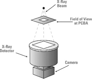
20.3.5. The New Jerusalem? X-Ray Inspection
Currently the fastest-growing inspection technique, X-ray inspection can detect defects that defy the line-of-sight constraint of optical systems. It can examine hidden components and solder joints on both surfaces of double-sided boards and can even inspect inner layers of multilayer boards. X-ray is the only available technique that can quantitatively analyze solder joints. Results can indicate problems with the solder and assembly processes, measuring such parameters as solder-joint accuracy, fillet height, solder volume (detecting both insufficient and excess solder), component existence and position, and polarized-capacitor orientation (by the position of the “slug”).
Figure 20.17 shows the geometry of a typical solder joint. The X-ray system can measure each of the noted features and compare them with a good-joint standard to permit a pass/fail decision. The gull-wing solder joint in Figure 20.18 will pass both electrical and X-ray inspection. In Figure 20.19, the joint shows an insufficient heel. This joint will pass electrical test because a connection exists. Nevertheless, it represents a potential reliability problem. Finding marginal faults such as this is one of X-ray inspection's strengths.
Figure 20.17. The geometry of a typical solder joint (Agilent Technologies).
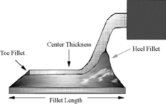
Figure 20.18. This solder joint will pass both X-ray inspection and electrical test (Agilent Technologies).

Figure 20.19. Contrast this joint with one in Figure 20.18. This one will pass electrical test because a connection exists but will fail the quantitative analysis of X-ray inspection because it represents a reliability problem for the product in the field (Agilent Technologies).

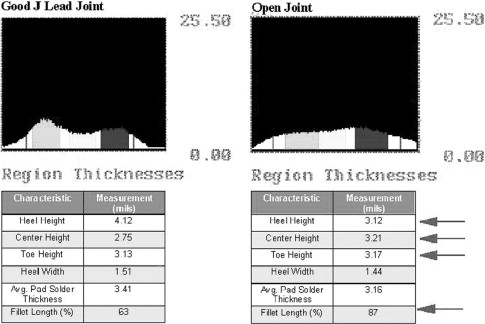
The X-ray system examines the joint, producing the image shown in Figure 20.20. Combining that information with data that calibrate the darkness of points in the image with solder thickness, along with some kind of image analysis, produces a quantitative profile of the joint. Figures 20.21 and 20.22 contain actual inspection results. Figure 20.21 contrasts an expected result for a good gull-wing joint with the result from a joint containing insufficient solder. In Figure 20.22, the inspection system detects an open on a J-lead solder joint.
Figure 20.20. The X-ray system combines calibration data and image-analysis techniques to construct a profile of the solder joint (Agilent Technologies).
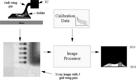
Figure 20.21. Contrasting results from a good gull-wing joint with those from a joint with insufficient solder (Agilent Technologies).

Figure 20.22. Results for a good J-lead joint and a comparable open joint (Agilent Technologies).
When considering adding X-ray inspection to their test arsenals, prospective users raise two particular issues. The most common question is: Is the equipment safe? That is, will harmful radiation escape into the workplace? The X-ray source is carefully shielded from the ambient environment. Governments have established safety standards, which today's equipment vastly exceeds. Study after study investigating X-ray inspection installations have shown no increase in radiation levels.
The second concern involves the migration to lead-free solder. Although solder produces only about 5% of the lead escaping into the environment (the majority comes from automobile batteries), environmental protection agencies around the world are pressuring the electronics industry to eliminate it. Lead-free solders present a considerable challenge. Higher melting points, a tendency toward brittleness, and other drawbacks to this approach will require careful consideration and solution. For X-ray inspection, however, lead-free solders present little problem. X-ray relies on the absorption characteristics of several heavy-metal elements (lead, bismuth, silver, tin) to ensure joint integrity. The technique can be adapted to the new solder alloys by recalibrating the inspection system and the image-analysis software.
Although X-ray inspection can find many faults that elude other methods, it is not a panacea either. It will not detect a wrong component unless it presents a very different X-ray profile from the correct one. X-rays cannot detect faulty and out-of-tolerance components and will not notice cracked solder joints that currently appear intact. For X-ray inspection to be effective, you have to combine it with some combination of process control, electrical test, and environmental-stress screening.
20.3.5.1. A Catalog of Techniques
X-ray inspection covers a broad range of capabilities. With manual equipment, a human inspector inserts a board into the system, then obtains the relevant image and makes the pass/fail decision.
The image that the inspector sees may contain only the basic X-ray snapshot, but it can also include metrology information or even complete quantitative analysis. Also, the software may enhance the image in some preset way or provide a level of image processing to make the inspector's decision easier and more consistent.
This approach offers economy, flexibility, and fast implementation. Cost will vary depending on the amount of infrastructure and software support but begins at less than $50,000. Manual inspection examines boards one at a time and usually looks only at critical areas, rather than at the entire board. It works better primarily for prototyping or during the ramp-up to full production, for random sampling for process monitoring, and where the nature of the board makes a full inspection unnecessary. Success depends on throughput requirements, and—depending on the level of available software assistance—may vary like other manual techniques, depending on the inspector's experience, the time of day, or the day of the week.
Semiautomated techniques include an X-ray system and sophisticated image-analysis software. This version inspects the board for device placement and solder-joint integrity based on preset gray levels. More expensive than manual alternatives, it requires longer lead times and a software model of the board for comparison. However, it also provides much greater consistency and generates far fewer false calls.
Most elaborate are the automated systems (so-called automated X-ray inspection, or AXI), where the software makes pass/fail decisions based on established heuristics. Long used for inspecting ball-grid arrays, it has become more popular in the past few years in production because of the difficulty determining board quality using more traditional test techniques. This alternative is faster than manual and semiautomated techniques. It is also considerably more expensive and requires longer startup times. In addition, depending on the throughput requirements of the production line, you may have to compromise between comprehensiveness and cycle time.
Programming X-ray systems can take two forms. Conventional programming involves an image of the board—either a constructed image or one obtained from a board simulation—and metrology tools to establish pass/fail criteria. Some systems learn from a known-good board (subject to the usual caveats) and can automatically locate, inspect, and evaluate each solder connection. This approach involves training the system to recognize all of the solder-joint geometries that it must inspect and storing the information in a library with corresponding thresholds and tolerances. The engineer can modify the library criteria to allow for deviations and customizations.
20.3.5.2. X-Ray Imaging
X-ray inspection falls into two broad categories, covering two-dimensional and three-dimensional techniques. Figure 20.23 shows two-dimensional, or transmission X-ray, where a stationary X-ray source looks directly through the board, inspecting both board sides simultaneously. Image intensity indicates depth of the feature under scrutiny. The approach works best with single-sided boards.
Figure 20.23. Transmission X-ray sees through the board, presenting it as a two-dimensional image (Agilent Technologies).
The mechanics of transmission X-ray equipment are considerably simpler than those of the more complex three-dimensional techniques. It is easier to implement and the equipment is less expensive. Test time is also faster, although proponents of three-dimensional approaches argue that a slower diagnostic time reduces the test-time advantage.
On the downside, transmission X-ray cannot easily distinguish features on double-sided boards because images of the two sides overlap. To compensate, some industry experts recommend staggering components on the top and bottom of the board, as Figure 20.24 illustrates.
Figure 20.24. Some industry experts recommend staggering components on top and bottom of double-sided boards
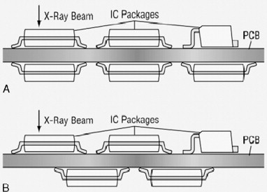
(Test and Measurement World (June 2000), p. 16. Used by permission).
Three-dimensional X-ray techniques, also known as X-ray laminography, tomography, and digital tomosynthesis, permit looking separately at two sides of the board by focusing on one surface while the other surface blurs into the background, as in Figure 20.25. It can even be used to examine inner layers of a multilayer board. Figure 20.26 shows a two-sided single in-line memory module (SIMM), its transmission X-ray image, and its three-dimensional image.
Figure 20.25. Keeping each plane of the board in focus (Agilent Technologies).

Figure 20.26. A two-sided single in-line memory module, its transmission X-ray image, and its three-dimensional image (Agilent Technologies).

Several different mechanisms can achieve the three-dimensional result. In the approach in Figure 20.27, the X-ray detector moves in a circle around the center of the board section under inspection, while the system mechanically steers the X-ray beam. Alternately, a steerable X-ray beam sends signals to eight stationary detectors. In either case, the system must locate the board surface exactly. The rotating-detector method scans the board with a laser to map the surface before inspection begins. The stationary-detector system performs a dynamic surface-mapping that avoids the test-time overhead of the laser step.
Figure 20.27. In this version, the X-ray detector moves in a circle around the center of the board section under inspection, while the system mechanically steers the X-ray beam (Agilent Technologies).

Three-dimensional X-ray can resolve board features individually, examining the two board sides independently—in one pass. Therefore, it can provide more precise, higher-resolution analysis than transmission methods can. On the other hand, it also requires a longer setup and longer test time, and is more expensive.
20.3.5.3. Analyzing Ball-Grid Arrays
One advantage of three-dimensional X-ray is the ability to analyze the quality of solder balls and connections on ball-grid arrays. In fact, inspecting BGAs represents the most common justification argument for adopting X-ray inspection. For some manufacturers, that is its only regular application. This inspection step looks for voids, out-of-location solder balls, excess solder, insufficient solder, and shorts. Figure 20.28 demonstrates how by examining slices at the board surface, the center of the ball, and the device surface, three-dimensional X-ray can create an accurate profile.
Figure 20.28. By slicing the solder ball on a BGA, an X-ray system can construct an accurate image of the whole ball (Agilent Technologies).

The voids in Figure 20.29 and the balls containing insufficient solder in Figure 20.30 will very likely pass electrical test. Nevertheless, these weak areas in the joint may succumb to mechanical and thermal stresses from handling and normal operation, and therefore represent reliability problems in the field.
Figure 20.29. Voids in a BGA (Agilent Technologies).

Figure 20.30. Insufficient solder in a BGA (Agilent Technologies).
Using multiple images, three-dimensional X-ray can also verify solder joints and barrel fill in plated-through holes (PTHs), as in Figure 20.31.
Figure 20.31. Using the three-dimensional technique allows examining the structure of plated through-holes (Agilent Technologies).

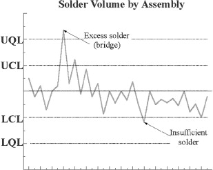
Because of the precision of its measurements, X-ray lends itself to process monitoring and feedback, even when conducted only on board samples. In Figure 20.32, UCL and LCL represent the upper and lower control limits, and UQL and LQL the upper and lower quality limits. The solder measurement lying outside the quality limit indicates a solder bridge—a short and, therefore, a fault that conventional test should also detect. One of the joints contains insufficient solder, but in this case it lies outside the control limits but within quality limits. This defect will pass electrical test, but X-ray inspection will generate a flag on the process that can initiate an investigation and correction to prevent future occurrences, reducing the number of future failures and thereby increasing manufacturing yields.
Figure 20.32. Looking at both upper and lower control limits (UCL and LCL) as well as upper and lower quality limits (UQL and LQL) allows the feeding of information back into the process to prevent future defects.
Deciding to include inspection in your test strategy represents the beginning—not the end—of the necessary planning. You still have to evaluate what to inspect (critical areas, samples, or all of every board), where in the process to inspect, and which technique or mix of techniques will likely furnish the best results.
20.4. Summary
The task of finding manufacturing defects in today's boards has become more difficult than ever before. In-circuit and other bed-of-nails techniques suffer from lack of access. For cellular-phone boards and other communications systems, the bed of nails itself creates problems because of its RF characteristics. Product evolution and the pace of change combined with skyrocketing complexity make fixture construction and program generation even more painful than in the past. Those same trends drastically reduce the likelihood that we will reach the “perfect process” within the foreseeable future.
Adding inspection to the “test” strategy permits verification when you cannot perform conventional test. It examines the board's structure, ensuring that you have built it correctly. Test determines on some level whether the board works.
Inspection can occur after paste printing, after parts placement, and after reflow. Visual inspection, automated-optical inspection, and laser and white-light methods work best after paste. After parts placement, most companies select manual inspection or AOI. After reflow, AOI and X-ray inspection—including automated X-ray inspection—produce the best results. Choosing among inspection methods, as with test, depends on the nature of the boards and the manufacturing process.