
Electrical Contact Resistance: Fundamental Principles
Only connect!
Howards End, E M Forster
CONTENTS
1.2 Electrical Constriction Resistance
1.2.2 Non-Circular and Ring a-Spots
1.2.4 Effect of the Shape of Contact Asperity on Constriction Resistance
1.3 Effect of Surface Films on Constriction and Contact Resistance
1.3.1 Electrically Conductive Layers on an Insulated Substrate
1.3.1.1 Calculation of Spreading Resistance in a Thin Film
1.3.2 Electrically Conducting Layers on a Conducting Substrate
1.3.2.1 Electrically Conducting Layers and Thin Contaminant Films
1.3.3 Growth of Intermetallic Layers
1.3.4 Possible Effect of Electromigration on Intermetallic Growth Rates
1.3.5 Electrically Insulating or Weakly Conducting Films
1.3.5.1 Growth Rate and Electrical Resistivity of Oxides of Selected Contact Materials
1.3.6 Fritting of Electrically Insulating Surface Films
1.4 Temperature of an Electrically Heated a-Spot
1.4.1 Voltage–Temperature Relation
1.4.4 Temperature Distribution in the Vicinity of an a-Spot
1.4.5 Deviation of the Voltage–Temperature Relation in an Assymetric Contact
1.4.5.1 Case I: Two Metals in Contact
1.4.5.2 Case II: A Metal in Contact with a Non-metal
1.4.6 Special Considerations on the “Melting” Voltage in Electrical Contacts
1.5 Mechanics of a-Spot Formation
1.6 Breakdown of Classical Electrical Contact Theory in Small Contact Spots
1.6.1 Electrical Conduction in Small a-Spots
1.6.1.2 Joule Heat Flow Through a-Spots
1.6.2 Observations of Breakdown of Classical Electrical Contact Theory in Aluminum Contacts
1.6.2.1 Experimental Data on Aluminum
1.6.3 Observations of Breakdown of Classical Electrical Contact Theory in Gold Contacts
1.6.4 Observations of Breakdown of Classical Electrical Contact Theory in Tin Contacts
1.7 Constriction Resistance at High Frequencies
1.7.1 Skin Depth and Constriction Resistance
1.7.2 Evaluation of Constriction Resistance at High Frequencies
1.7.3 Constriction versus Connection Resistance at High Frequencies
All solid surfaces are rough on the microscale. Surface microroughness consists of peaks and troughs whose shape, variations in height, average separation, and other geometrical characteristics depend on fine details of the surface generation process [1]. Contact between two engineering bodies, thus, occurs at discrete spots produced by the mechanical contact of asperities on the two surfaces, as illustrated in Figure 1.1. For all solid materials, the area of true contact is, thus, a small fraction of the nominal contact area, for a wide range of contact loads [1,2]. The mode of deformation of contacting asperities is either elastic, plastic, or mixed elastic–plastic depending on local mechanical contact stresses and on properties of the materials, such as elastic modulus and hardness. In a bulk electrical interface where the mating components are metals, the contacting surfaces are often covered with oxide or other electrically insulating layers. Generally, the interface becomes electrically conductive only when metal-to-metal contact spots are produced, that is, where electrically insulating films are ruptured or displaced at the asperities of the contacting surfaces. In a typical bulk electrical junction, the area of electrical contact is, thus, appreciably smaller than the area of true mechanical contact.
In a bulk electrical junction, the electric current lines become increasingly distorted as the contact interface is approached and the flow lines bundle together to pass through the separate contact spots (or “a-spots"), as illustrated in Figure 1.1. Constriction of the electric current by a-spots reduces the volume of material used for electrical conduction and thus increases electrical resistance. This increase in resistance is defined as the constriction resistance of the interface. Often, the presence of contaminant films of relatively large electrical resistivity on the contacting surfaces increases the resistance of a-spots beyond the value given by constriction resistance. The total interfacing resistance provided by the constriction and film resistances determines the contact resistance of the interface.
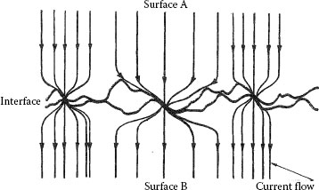
FIGURE 1.1
Schematic diagram of a bulk electrical interface.
The present chapter reviews some fundamental properties of electrical contacts and updates the reader on the results of recent research. The review focuses on the effect of constriction of current flow on electrical resistance, interdiffusion processes at electrical interfaces, the relationship between the drop in electrical potential and temperature in an electrical contact (the so-called voltage–temperature relation), sintering, softening, and melting in contact spots, the effect of deformation of asperity on contact resistance and so on. The chapter thus attempts to update the reader on similar topics covered in Holm’s classic text [3].
1.2 Electrical Constriction Resistance
For the sake of simplicity, the evaluation of constriction resistance generally assumes a-spots to be circular. This assumption provides an acceptable geometrical description of electrical contact spots “on the average” where the roughness topographies of the mating surfaces are isotropic. The assumption becomes invalid where the mating surfaces are characterized by a directional roughness, as in rolled metal sheets or extruded rods, where the shape of the a-spot would be characterized by a large aspect ratio. Although most of the properties of electrical contacts are usually discussed in terms of circular a-spots, the constrictive properties of contact spots of other shapes are addressed below for the sake of completeness. Unless otherwise stated, all descriptions given below assume a DC electric current. The evaluation of constriction resistance under AC conditions will be discussed later in the chapter.
The mathematical problem of constricted current flow is treated in several textbooks, for example, [4]. For a circular constriction located between two semi-infinite solids (one of such surfaces shown in Figure 1.2a), it is found that the equipotential surfaces in the contact members consist of ellipsoids defined by the equation
r2a2+μ2+z2μ2=1
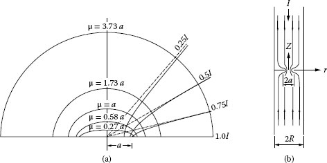
FIGURE 1.2
(a) Equipotential surfaces and current flow lines near an electrical constriction; the parameter μ is the vertical axis of the vertical ellipsoidal surface. The curves corresponding to current flow identify the boundaries enclosing the current fraction indicated, (b) Electrically conducting cylinder of radius R carrying a circular constriction of radius a.
where μ is the length of the vertical semi-axis of the ellipsoid and (r, z) are cylindrical coordinates. The resistance between the equipotential surface with semi-axis μ and the constriction is given as [3,4]
(1.1) |
where ρ is the resistivity of the conductor. Sufficiently far away from the constriction where μ is very large, the constriction resistance between the equipotential surface and the constriction, that is, the spreading resistance, is given as
(1.2) |
The total constriction resistance for the entire contact is, thus, twice the spreading resistance or
(1.3) |
Equations 1.2 and 1.3 are widely used in the literature and in problems relating to the design of electrical contacts. Later in this chapter, we shall see that the general form of Equation 1.3 is true for monometallic contacts even when they are an agglomeration of a-spots that are not necessarily circular. If the upper and lower half of a contact consist respectively of materials with resistivity ρ1 and ρ2, the spreading resistance associated with each half of the contact is then ρi/4a where i = 1,2. The electrical constriction resistance, then, becomes
Rc={ρ1+ρ2}4a
TABLE 1.1
Electrical Resistance of a Circular Constriction in a Copper–Copper Interface
a-Spot Radius (μm) |
Constriction Resistance (Ω) |
0.01 |
0.88 |
0.1 |
8.8 × 10⁻² |
1 |
8.8 × 10⁻³ |
10 |
8.8 × 10⁻⁴ |
It is instructive to evaluate the magnitude of contact resistance as a function of the radius of the a-spot for a circular constriction in a copper–copper interface (ρ = 1.75 × 10⁻⁸ Ω m). This is illustrated in Table 1.1.
Note that the resistance of a constriction 10 μm in radius is approximately 1 mΩ. This is very small! As will be shown later in this chapter, the passage of an electric current of 20 A through such a constriction will not cause appreciable heating within this constriction. Similarly, a constriction 100 μm will be able to pass a current of 200 A without significant heating. Thus, the area of electrical contact between two surfaces need not be large to “short out” the electrical interface, that is, to generate an electrical contact of acceptably low resistance.
The electrical resistance Rc presented by a circular constriction in a cylindrical conductor of radius R, as illustrated Figure 1.2b, can be calculated from a solution of Laplace’s equation using appropriate boundary conditions [5,6]. It may be shown that the electrical contact resistance is accurately given as
Rc={ρ2a}(1−1.41581{aR}+0.06322{aR}2+0.15261{aR}2+0.19998{aR}4) |
(1.4) |
Equation 1.4 reduces to Equation 1.3 where the constriction radius becomes small in comparison with the cylinder diameter. Figure 1.3 shows the measured and calculated dependence of Rc on the ratio a/R [7]. The agreement between the measured and calculated values reveals the reliability of Equation 1.4 over the entire range of values of a/R. This reliability is often important in applications where a/R is close to unity, as in cylindrical bus bar junctions carrying large electric currents. In these cases, a small change in constriction radius may translate into a significant change in constriction resistance and into a correspondingly significant change in power dissipation. The current density distribution in the constriction is given by the expression [5,6]
(1.5) |
where I is the electric current, r is the radial location within the constriction and m is a factor that deviates significantly from unity only for values of a/R greater than approximately 0.5 [6].
1.2.2 Non-Circular and Rring a-Spots
As mentioned earlier, under conditions where the microtopography of the surfaces of the mating bodies is not isotropic, the assumption that a-spots may be treated as circular “on the average” may not be valid and could lead to erroneous conclusions. This section examines the effect of a departure from circular symmetry on the constriction resistance of a single a-spot.
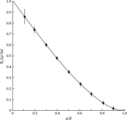
FIGURE 1.3
Measured and calculated (full curve) constriction resistance in a constricted cylinder of radius R, as a function of a/R. (From RS Timsit, Proc 14th Int Conf Elect Cont, Paris, 21, 1988 [7].)
It is shown by Holm [3] that the spreading resistance Rc (a, b) associated with an elliptical a-spot with semi-axes a and b is given as
Rc(a,b)=ρ2π∞∫0dμ[(a2+μ2)(b2+μ2)]1/2
and may be expressed as
(1.6) |
where γ =√a/b is the square root of the aspect ratio of the constriction, the function f(γ) is a form factor and the quantity ac is the radius of a circular spot with area identical to that of the elliptical a-spot. The form factor is shown graphically in Figure 1.4 and decreases in value from 1 to 0 as the aspect ratio increases from 1 to ∞, that is, as the contact spot becomes increasingly elongated. Note that the constriction resistance decreases slowly as the aspect ratio increases from 1 to approximately 10. The constriction resistance of an elliptical a-spot located between two semi-infinite solids is given as 2Rs (a, b). Aichi and Tahara [8] measured the spreading resistance of rectangular a-spots using an electrolytic bath. Their data is illustrated in Figure 1.5. A regression analysis of the data of Figure 1.5 indicates that the spreading resistance Rs is given empirically as
(1.7) |
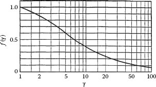
FIGURE 1.4
Dependence of the form factor f(γ) on the aspect ratio γ. (With kind permission from Springer Science+Business Media: Electric Contacts, Theory and Applications, 2000, R Holm [3].)
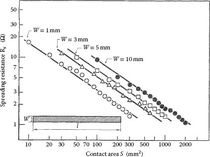
FIGURE 1.5
Dependence of spreading resistance on the area of the rectangular a-spot; the area is given as wl where w and l are, respectively, the width and length of the spot. The resistivity of the electrolytic bath is 175 Ω mm. (From H Aichi and N Tahara, Proc 20th Int Conf Elect Cont, Nagoya, Japan, 1, 1994 [8]. With permission.)
where S is the area of the rectangular constriction, when the aspect ratio of the constriction is 10 or larger. The quantity k is a parameter that depends on the width of the constriction. It varies from 0.36 to approximately 1 (when S and ρ are expressed respectively in mm2 and Ω mm) as the width of the constriction increases from 1 mm to 10 mm. The constriction resistance of a rectangular a-spot located between two semi-infinite solids is, thus, given as 2Rs. Note that Equation 1.7 may be expressed as
(1.8) |
where w and l are the width and length of the constriction respectively, L=√wl is the width of a square constriction of identical area, and k′ = 4k. Equation 1.8 is of the same general form as Equation 1.6 and confirms the general predictions of Equation 1.6 that the resistance decreases slowly with increasing aspect ratio l/w. If the aspect ratio is 10 or greater, Equations 1.6 and 1.8 predict similar values of the spreading resistance. Recall that Equation 1.8 does not hold true for aspect ratios much smaller than 10.
A rigorous numerical evaluation of the spreading resistance of square a-spots, and of a-spots consisting of circular and square rings, was carried out by Nakamura [9]. This work indicates that the spreading resistance of a square constriction with side length 2L and located between two semi-infinite conductors is given as
Rs=0.434ρL
Note that this expression yields Rs values about 70% larger than those obtained from relation 0.25ρ/a for the spreading resistance of a circular constriction, for identical values of ρ/L and ρ/a. More generally, the spreading resistance of square and circular ring-shaped constriction illustrated in Figure 1.6a is found to be given as
Rs=R0F(ζ)−1
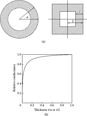
FIGURE 1.6
(a) Square and circular ring constrictions (b) Form factor F(ζ) for the ring constrictions shown in (a); the relative spreading conductance is given as (ρ/4a)/Rs for the circular ring, and as (0.434ρ/L)/Rs for the square ring. The difference between the two curves is too small to be seen in the plot. (From M Nakamura, IEEE Trans Comp Hyb Manuf Tech, CHMT-16: 339, 1993 [9]. With permission.)
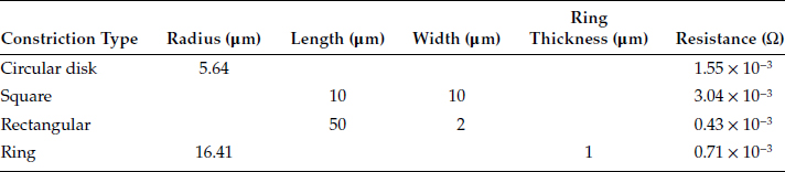
TABLE 1.2
Resistance of Constrictions of the Same Area (100 μm2) and Different Shapes at a Copper–Copper Interface
where Ro is the spreading resistance of the full circular or square a-spot, and F(ζ) is a conductance form factor. In the case of the circular ring constriction, ζ = t/a where t and a are the thickness and outer radius respectively. In the case of the square constriction, ζ = t/L. The form functions F(ζ) for the square and circular rings are essentially identical and are shown in Figure 1.6b. Note that the difference in the relative spreading resistances Rs/[ρ/4a] and Rs/[0.434ρ/L] for the circular and square ring is too small to be evident in the plot (Figure 1.6b).
The expressions for constriction resistance of a-spots that are rectangular, circular ring or rectangular ring shaped find application where contacting surfaces are specially textured, as for example, in many types of power utility connectors where surfaces carry pyramidal knurls that penetrate conductors to increase friction forces. The a-spots are, then, square or rectangular. Ring-shaped constrictions are rarer but occur where one contacting surface carries a highly conductive cladded layer on a knurled surface. In this instance, passage of electric current through the constriction occurs largely through the cladding material of the knurl in contact with the mating surface. Table 1.2 compares the resistance of constrictions of identical areas (100 μm2), but having different shapes in a copper–copper interface (ρ = 1.75 × 10⁻⁸ Ωm). Note from Table 1.2 that the constriction resistance is significantly affected by the shape of the constriction.
In practice, an electrical junction comprises a multitude of contact a-spots through which electric current passes from one connector component to another. The a-spots are formed from the contact of asperities on the mating surfaces as illustrated in Figure 1.1. The number of asperity contacts increases with normal load as illustrated in the series of micrographs of Figure 1.7 reproduced from the work of Thomas and Probert [10]. In practice, contact between nominally flat surfaces occurs at clusters of a-spots. The positions of the clusters are determined by the large-scale waviness of the contact surfaces, and the a-spots by the small-scale surface roughness. Contact resistance is, then, determined by the number and dimensions of the a-spots and by the grouping and dimensions of the clusters. Although mechanical contact occurs at many contact spots, electrically conducting a-spots are generated only if surface insulating layers such as oxide films are fractured or dispersed. Because the fracture mode of oxide films may depend on the deformation mode of the contacting asperities, that is, elastic or plastic deformation, the number of metal-to-metal a-spots is generally difficult to predict and may be appreciably smaller than the number of asperities that made initial contact with the surface insulating films.
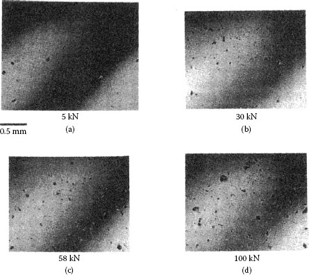
FIGURE 1.7
Optical micrographs showing the increase in the number of contact spots on a soft but smooth steel optical flat following contact with a sand-blasted tool steel surface, with increasing load; the contact spots represent imprints of contacting asperities on the soft but smooth optical flat. (From TR Thomas and SD Probert, J Phys D: Appl Phys 3: 277, 1970 [10]. With permission.)
For the sake of ease of calculation, the collective action of metal-to-metal a-spots is generally treated in terms of the properties of circular spots. In the simplest case of a large number n of circular a-spots situated within a single cluster, it was shown by Greenwood [11] that, to a good approximation, the contact resistance is given as
(1.9) |
where a is the mean a-spot radius defined as Σai/n (ai is the radius of the ith spot) and α is the radius of the cluster sometimes defined as the Holm radius.
Table 1.3 shows the relative magnitudes of the two terms in Equation 1.9 calculated by Greenwood [11] for the regular array of 76 identical a-spots illustrated in Figure 1.8, as the a-spot radius is increased. In the calculation, the spot spacings are taken as one and the maximum a-spot radius is 0.5. Note that the cluster resistance 1/2α exceeds the a-spot resistance when the a-spot radius increases beyond approximately 0.05. The contact radius of a single spot of the same resistance is, then, given to a reasonable approximation by the Holm radius, α. The radius of equivalent single contacts and the Holm radius for a variety of a-spot distributions, also calculated by Greenwood [11], are illustrated in Figure 1.9. Note in each case that the circular area defined by the Holm radius (i.e., the Holm circle) provides an excellent representation of the area over which electrical contact occurs. These results are significant because they suggest that the details of the number and spatial distribution of the a-spots are not important to the evaluation of contact resistance in many practical applications where electrical contact occurs reasonably uniformly over the nominal contact area, that is, in the absence of electrically insulating surface films. This conclusion is supported by Nakamura and Minowa [12] and Minowa et al. [13] who used finite element analysis and Monte Carlo techniques to examine the effect of a-spot distribution on electrical resistance. They found that the resistance of an interface characterized by a fixed electrical area was not significantly affected by the a-spot locations within the selected nominal contact area. Only if the a-spot distribution was limited to areas close to the periphery of the nominal geometrical interface was contact resistance affected appreciably. Even under these circumstances, resistance increased only by a factor of approximately two over the resistance produced by concentrating all the a-spots at the centre of the nominal area of electrical contact. The results of the investigations mentioned above suggest that for many engineering purposes, knowledge of the Holm radius may be sufficient to estimate contact resistance. As a first approximation, the Holm radius may be estimated from the true area of contact, A, as [A/π]1/2.
TABLE 1.3
Effect of a-Spot Radius on Constriction Resistance 1/2na and Holm Radius α
a-Spot Radius |
a-Spot Resistance 1/2na |
Holm Radius α |
Cluster Resistance 1/2α |
Radius of Single Spot of Same Resistance |
0.02 |
0.3289 |
5.34 |
0.0937 |
1.18 |
0.04 |
0.1645 |
5.36 |
0.0932 |
1.94 |
0.1 |
0.0658 |
5.42 |
0.0923 |
3.16 |
0.2 |
0.0329 |
5.50 |
0.0909 |
4.04 |
0.5 |
0.0132 |
5.68 |
0.0880 |
4.94 |
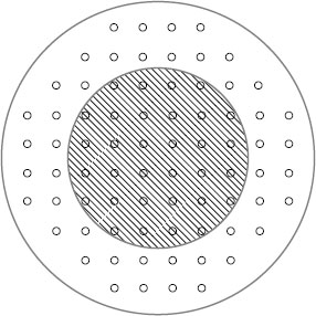
FIGURE 1.8
Regular array of a-spots; the shaded area is the single continuous contact with the same resistance; the outer circle is the Holm radius of the cluster. (From JA Greenwood, Brit J Appl Phys 17: 1621, 1966 [11]. With permission.)
Because the true area of contact is smaller than the apparent area of contact, a-spots must support local pressures that are comparable with the strengths of the materials of the contacting bodies. It is generally accepted that the true contact area is controlled by the plastic deformation of the asperities projecting from the surface. Although Archard [14] proposed an elastic theory of contact, Greenwood and Williamson [2] have shown that deformation of the asperity is generally plastic in most practical applications. Bowden and Tabor [15] proposed that the contact pressure on contact asperities is equal to the flow pressure of the softer of the two contacting materials and the normal load is then supported by plastic flow of the softer asperities. Under this assumption, the area of mechanical contact, Ac, is related to the load F applied to the electrical interface and to the plastic flow stress (or hardness) H of the softer material as
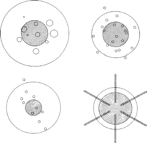
FIGURE 1.9
Clusters of a-spots with corresponding radius of equivalent single contact (shaded area) and Holm radius (outer radius). (From JA Greenwood, Brit J Appl Phys 17: 1621, 1966 [11]. With permission.)
(1.10) |
Expression 1.10 is extremely important and relevant for the interpretation of measurements of electrical contact resistance, as will be evident shortly. It states that the true area of mechanical contact between two surfaces is independent of the area of nominal contact of the surfaces; that is, Ac= F/H depends only the contact force and the hardness of the contacting bodies, and is independent of the dimensions of the contacting objects. This is a remarkable statement. The physical origin of Equation 1.10 may be elucidated through the following simple argument: consider two sets of coupons of identical materials but of different dimensions, say 1 cm2 and 10 cm2 respectively, subjected to the same contact load, F. If the materials have the same surface finish, they will carry the same surface density of asperities. Thus, if the true contact area between the smaller coupons is generated through n asperities, the true contact area between the larger coupons is necessarily generated through 10n asperities. The average mechanical load developed at each asperity in the smaller interface is, then, F/n, whereas the same quantity in the larger interface is only F/10n. If deformation of the asperity is fully plastic, the area of contact at each asperity in the smaller interface will be 10 times larger on the average than in the larger interface, but the total contact area is identical in the two interfaces. Hence, Equation 1.10 is valid under conditions of plastic deformation.
If the electrical interface does not carry electrically insulating films and is characterized by a sufficiently large number of a-spots distributed within a Holm radius α, the data of Table 1.3 suggest that the contact resistance can be approximated as
Rc=ρ2α
and Ac=ηπα2, where η is an empirical coefficient of order unity for clean interfaces. Using Equation 1.10, the contact resistance may be expressed as
(1.11) |
Expressions of the form as in Equation 1.11 have been used by several workers [3,15,16,17]. The general validity of this expression over a wide range of mechanical loads appears to be consistent with much published experimental data for a variety of contact materials (see [18,19,20,21,22,23]) as illustrated in Figures 1.10 through 1.12. The presence of interfacing contaminant films modifies the right-hand side of Equation 1.11 by the addition of a new term, as will be shown later.
The relative simplicity of Equation 1.11 and the broad agreement between its predictions and the experimental data mask the underlying complexity of the physical phenomena involved in the generation of a bulk electrical interface. The decrease in contact resistance with increasing mechanical load depicted in Figures 1.10 through 1.12 stems from a combination of several factors, the most important ones being:
(1) An increase in the number of contacting surface asperities as the nominal surfaces are brought closer together under the influence of an increasing load, (2) A permanent flattening of the contacting asperities, which reduces the constriction resistance associated with each a-spot and thus reduces the overall contact resistance, and (3) Work-hardening of the deformed contact asperities. The last effect decreases the rate at which contacting asperities flatten, and thus, reduces the rate at which new asperities are brought into play as the load is increased further. Note in Figures 1.10 and 1.11, contact resistance increases relatively slowly with decreasing load, after application of the initial load. This stems from permanent flattening and adhesion of the asperity following contact.
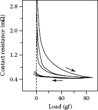
FIGURE 1.10
Contact resistance as a function of load for nominally clean gold electric contacts in air. The arrows show the direction of load application. (From RE Cuthrell and DW Tipping, J Appl Phys 44: 4360, 1973 [20].)
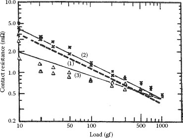
FIGURE 1.11
Contact resistance as a function of load for surfaces consisting of Ag90Pd10. Curve (1), results calculated using Equation 1.11; curves (2) and (3), experimental results (x, first test load increased; Δ, first test, load decreased). (From Y Watanabe, Wear 112: 1, 1986 [22].)
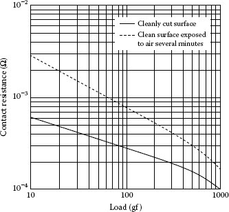
FIGURE 1.12
Contact resistance as a function of load for freshly cut copper and crossed rods and for identical rods after long exposure to air. (From LP Solos, Elect Cont-1962: Eng Sem Elect Cont, University of Maine, June 1962 [23].)
Mathematical models that attempt to explain the behaviors depicted in Figures 1.10 through 1.12 in terms of mechanical deformation properties of single asperities [1,2,14,24] predict a relationship between contact resistance and mechanical load that does not differ appreciably from that given in Equation 1.11. This remarkable result suggests that the details of deformation of single asperities are relatively unimportant and that assumptions used in the derivation of Equation 1.11 are not overly simplistic. Equation 1.11 is widely used by design engineers to estimate the expected constriction resistance for selected values of hardness and contact force in an electrical contact. This estimate generally agrees to 20% or better with actual measured values.
1.2.4 Effect of the Shape of Contact Asperity on Constriction Resistance
The surface asperities of solid bodies exhibit a wide variety of geometrical shapes. In general, the surface in the immediate vicinity of an a-spot is not parallel to the average plane of the electrical interface, as illustrated in Figure 1.13. It was shown by Sano [25] that the spreading resistance Rθ associated with an a-spot generated by an asperity making an angle θ with the mating surface, as shown in Figure 1.13, is given as
(1.12) |
where a is the radius of the contact spot and ze is the normal distance from the contact interface. Equation 1.12 was derived under the assumption that the current distribution within the constriction is given by Equation 1.5 with m= 1, for all values of θ. Since this cannot be valid for large θ (for example, for θ ~ 90° where the current distribution is constant across the constriction), Equation 1.12 is valid only for relatively small values of θ. For values of ze large in comparison with a, Expression 1.12 becomes
Rθ=ρ4atan{π+2θ4}
The right-hand side of this relation reduces to the well-known expression for the spreading resistance of a circular constriction, Ro = ρ/4a, for θ = 0. Figure 1.14 shows the variation of the ratio Rθ/Ro with increasing θ, as evaluated from Equation 1.12. The data indicate that the effect of the slope of the asperity for values of θ as large as 10° is negligible. This is an important result since it indicates that the presence of knurls, which are often embossed on connector surfaces to increase friction with the conductor, has a negligible effect on contact resistance unless the knurl slope θ is appreciably larger than 10°.
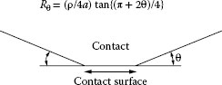
FIGURE 1.13
The a-spot produced by the contact of a conical asperity making an angle θ with the mating surface.
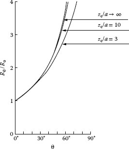
FIGURE 1.14
Variation of the ratio Rθ/Ro with increasing θ. (From Y Sano, J Appl Phys 58: 2651, 1985 [25]).
1.3 Effect of Surface Films on Constriction and Contact Resistance
1.3.1 Electrically Conductive Layers on an Insulated Substrate
Because thin conducting films have becomes ubiquitous as contact platforms in semiconductor-based devices, it has become increasingly important to understand electrical constriction resistance in thin films deposited on an electrically insulated substrate or a substrate of substantially larger resistivity than that of the thin film. Such contacts would occur, for example, in a contact between a microwire and a thin film on a semiconductor. In these cases, optimization of configurations of the electrical contact with thin films would minimize contact resistance and associated factors such as Joule heating at the contacts. It is for this reason that constriction resistance in thin films is addressed in some detail in this section.
1.3.1.1 Calculation of Spreading Resistance in a Thin Film
Expression 1.2 for the electrical spreading resistance of a circular constriction in a bulk interface stems from spreading of electric current flow lines from the constriction towards the bulk of the conductor as illustrated in Figure 1.15a. In a conducting thin film, spreading resistance stems from the resistance to electrical flow only in the conducting region where the current spreads in the immediate vicinity of the constriction in the film as illustrated in Figure 1.15b, that is, in the cylindrical region defined by r ≤ rA. Thus, spreading resistance in a thin film is not described by Equation 1.2 and deviations from this relation are expected to be particularly significant where the ratio of the constriction radius a to the film thickness LF is of the order of one or larger, that is, for thin films. In this situation, the current streamlines bend sharply away from the constriction edge and flow parallel to the film boundaries after a short distance r ~ rA. In contrast, spreading occurs over a much larger region in the case of the bulk (i.e., two semi-infinite solids in contact) in Figure 1.15a. In Figure 1.15b, the resistance presented by the thin film in the region r > rA where the current streamlines in the radial direction are parallel to the horizontal boundaries of the films, does not contribute to constriction resistance. The resistance to radial flow in a hollow cylinder with an inner radius a, an outer radius b, and a length LF is given as [3]
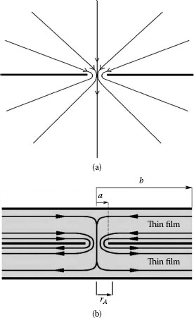
FIGURE 1.15
(a) Spreading of current streamlines in two “bulk” conductors in contact over a circular spot of radius a. The spreading resistance in each conductor is given by Equation 1.2. (b) Spreading of current streamlines near a constriction between two thin films.
(1.13) |
and will be designated as “bulk” resistance. Timsit [26] provided an analytical expression for the resistance RT between the center of a circular constriction of radius a located on one flat side of a cylinder of height LF and the outer circular surface of radius b of the cylinder as illustrated in the inset of Figure 1.16. The expression is
(1.14) |
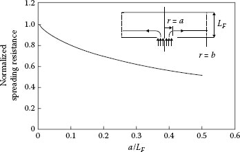
FIGURE 1.16
Variation of the normalized spreading resistance RN with increasing constriction radius; the constriction radius is normalized to the film thickness LF. Inset: Flow of electric current in a cylindrical film of outer radius b and thickness LF, from a constriction of radius a. (From RS Timsit, IEEE Trans Comp Pack Tech 33: 636, 2010 [26].)
where J1(x) is the Bessel function of order one and λn is the nth root of the Bessel function of zero order, J0(x). Because the current distribution within the constriction was approximated by Equation 1.5 (with m = 1), Expression 1.14 was valid only for values of a/LF < 0.5. The spreading resistance RS in the thin film was then evaluated as
(1.15) |
The spreading resistance evaluated from Equations 1.14 and 1.15 and normalized as RN to the spreading resistance in an infinitely thick film that is, RN = RS(ρ/4a), is shown in Figure 1.16. The graph illustrates variations of the normalized spreading resistance with the normalized constriction radius a/LF and indicates that the spreading resistance is identical with the value given by the classical expression, ρ/4a, that is, RN ≈ 1, only for small values of a/LF (≤ 0.01).This result was found to be independent of the actual values of a and LF and was verified for a wide range of values of L/b. These results show trends similar to those published by Norberg et al. [27] who evaluated contact resistance in thin films on the basis of approximations based on empirical modifications of Equation 1.3, which precludes a direct comparison with the results in Figure 1.16. The data of Figure 1.16 indicate that the spreading resistance decreases to about one-half the classical value at a/LF ~ 0.5. The result that spreading resistance in a radially conducting film decreases with decreasing film thickness appears counter-intuitive since the resistance of a solid conductor increases with decreasing thickness. An explanation for this will be given later in relation to the behavior of constriction resistance at high signal frequency.
1.3.1.1.1 Remarks on the Calculation of Spreading Resistance
In the evaluation of spreading resistance from Equation 1.15, it is important to note that the choice of the bulk resistance RB is somewhat arbitrary, because the current flow lines do not bend sharply and become parallel to the thin-film surface exactly at a radial distance r = a. As illustrated schematically in Figure 1.15b, the transition in current flow direction is completed at a radius rA > a. Because the radius rA is unknown a priori, the definition of the spreading resistance RS in Equation 1.15 can only be considered as approximate. In a series of papers, Zhang et al. [28,29,30,31] evaluated numerically the spreading resistance of various 2D and 3D thin-film contact geometries for a wide range of values of both a/LF and the ratio of resistivity of the contacting materials. The evaluations were performed to great accuracy using the MAXWELL 2D and 3D simulation codes [28]. For rectangular contact geometries with 2D symmetry, the results agreed exactly with the spreading resistance expressions of Hall [32,33] based on conformal mapping. For the cylindrical thin film illustrated in Figure 1.15, the authors summarized the dependence of the normalized spreading resistance RN on y = a/LF by the following best-fit expressions
RF{y}=1−2.2968y+4.9412y2−6.1773y3+3.811y4−0.8836y5,0.001≤y≤1 |
(1.16) |
and
(1.17) |
Equations 1.16 and 1.17 are independent of the outer film radius b since the bulk film resistance given by Equation 1.13 is subtracted out. The results of these computer simulations also confirmed the validity of Equation 1.14 to values of a/LF ~ 0.5. Additional work by these authors and Timsit [31] extended the evaluation of RN for values of a/LF approaching 100. The results of all numerical evaluations are shown in Figure 1.17. They indicate that the normalized spreading resistance, based on the spreading resistance calculated using Equation 1.14, decreases from the value of 1 to reach a limiting value of 0.28 as LF approaches zero that is, as a/LF becomes large. This limiting value is independent of the film outer radius b. The result of a non-vanishing RN for a vanishing film thickness was unexpected, but may be understood from an examination of current flow lines into the thin film, as shown in Figure 1.18.
The current flow lines of Figure 1.18 were calculated for the case of a/LF = 10.1 [31] and show unambiguously that the streamlines are concentrated near the edge of the constriction and curve inwards significantly at radial distances smaller than a. The calculations in [31] show that the current streamlines in the thin film are concentrated in a radial region defined by a′ and a with
(1.18) |
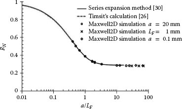
FIGURE 1.17
Normalized thin-film spreading resistance RN as a function of a/LF, for the cylindrical structure in Figure 1.15. The solid line is calculated from Equation 1.15, synthesized from the results of series expansion calculations [30]. The dashed line and the symbols describe respectively the results of Timsit’s calculations [26] and the data from the MAXWELL 2D simulation. Three sets of simulation were performed. The first set was fixed at a = 20 mm (circles), and varying LF from 20 mm to 1 mm; the second set was fixed at LF = 1 mm (crosses), and varying a from 30 mm to 70 mm; the third set was fixed at a = 0.1 mm (diamonds), and varying LF from 0.25 mm to 0.0015 mm.
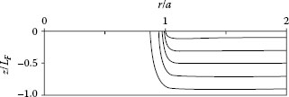
FIGURE 1.18
Field lines in the radial direction in the cylindrical thin film in the inset of Figure 1.16, calculated from the series expansion method [31], for the case of a/LF = 10.1. (From P Zhang et al., IEEE Trans Comp Pack Tech 39: 1936, 2012 [31].)
Crowding of the current and the ensuing spreading inward in the region r ≤ a occurs independently of the value of film thickness, LF and describes the effect responsible for the normalized spreading resistance of 0.28 for any non-zero value of a even as LF tends to 0. Thus, a non-zero value of normalized spreading resistance would be obtained even if the film is very thin, since in this case spreading of the current line would occur within the volume defined by r ≤ a.
There is an additional important result from the analyses in [28,29,30,31]. The crowding of the current streamlines near the edge between a′ defined in Equation 1.18 and a could lead to significant ohmic heating in this region. Such enhanced ohmic heating is well-known in bulk electrical contacts [34], on the basis of the distribution of current density in the constriction as given by Equation 1.5. Current crowding in metal–semiconductor contacts can lead to significant ohmic heating and deleterious effects on contact resistance [35]. There are differences between metal–metal and metal–semiconductor contacts. For example, in the transmission line model of a metal–semiconductor contact [35,36], the length over which most of the current from a contact into a semiconductor thin film flows is called the transfer length, LT. From Equation 1.18 and Figure 1.18, it may be argued that LT∼0.44LF for the present cylindrical thin-film model, and this transfer length is only due to the fringing fields. In the transmission line model [35], there is another component of transfer length, neglecting the fringing fields, which is approximately given by LT2=(R′C/R′S)1/2, where R′S=ρ/LF is the sheet resistance (in Ωm−2) in the thin film semiconductor under the contact, and R′C=ACρC, where AC is the contact area of the film with the semiconductor, and ρC is the so-called contact resistivity. The resistivity ρC arises from the metal–semiconductor barrier so that in the case of a metal film ρC = 0, yielding LT2 = 0 in the conventional transmission line model [33]. The transmission line model does not include the effect of fringing fields described in this section, but in the light of Equation 1.18, such an effect should be taken into account.
Finally, we point out that calculations of spreading resistance for various thin-film configurations have been carried out by other workers [37,38,39,40,41,42], but the boundary and contact conditions were not the same as those treated in [28,29,30,31]. Experimental measurements of constriction resistance are difficult and some results compare favorably with theory [43,44,45]. A full comparison between theory and experiment will require an appreciation of the limits of application of the models described above.
1.3.2 Electrically Conducting Layers on a Conducting Substrate
The presence of a film at the interface of an electrical junction affects contact resistance in a variety of ways. If the film is present initially on one of the contact surfaces and is electrically conducting, the constriction resistance of an a-spot is either decreased or increased relative to the resistance produced by the identical a-spot on the uncoated surface, depending on the electrical resistivity of the film material relative to that of the substrate. A change in mechanical hardness due to the presence of the film may also affect contact resistance as suggested by Equation 1.11. If the interfacing layer is formed by the interdiffusion of dissimilar materials across the contact, contact resistance will often increase through the formation of electrically resistive intermetallic compounds. If the film is electrically insulating or only weakly conducting, a good electrical contact is established only if the film is mechanically disrupted to allow the formation of metal-to-metal junctions. This section reviews the effect of electrically conducting layers such as electroplated layers, electrically resistive layers such as contaminant surface films and electrically insulating interfacing layers on constriction and contact resistance.
1.3.2.1 Electrically Conducting Layers and Thin Contaminant Films
Electrically conducting coatings (electroplates) are often used to minimize electrical contact resistance. Contact resistance may also be reduced through the action of several mechanisms such as a decrease in surface hardness, large electrical conductivity of the electroplate relative to that of the substrate, elimination of electrically insulating surface oxide films, and so on. Conducting coatings are also used to protect contact surfaces against tarnishing and oxidation, corrosion, mechanical wear, and the like. Because of its resistance to oxidation and mechanical wear, gold is the plating material of choice for producing reliable electrical contacts in copper–base electrical connectors. However, environmental testing involving exposure to high humidity and severely polluted laboratory or out-of-door environments [6,47] show that even gold coatings do not protect against corrosion if they are porous (see Chapters 2 and 3). These tests also show that the gold layer must be sufficiently thick to be pore-free and hence to perform satisfactorily in electrical connectors. Because this is generally not cost-effective, other plating materials have been examined as a replacement for gold. This replacement is not straightforward. For example, substitution by palladium has been hampered by the tendency of this metal to tarnish and form frictional polymers [48]. Many alloys have been evaluated, such as palladium–silver, tin–lead, tin–nickel, cobalt–gold, and so on. (see for example [49,50,51,52,53]). For aluminum-base connectors, the use of tin and nickel platings has been considered [54] to mitigate the effects of corrosion and surface oxidation on the electrical connectibility of aluminum. The introduction of plated layers in a connector system is discussed in detail in Chapter 7. In this section, we focus on the models used in the interpretation of contact resistance properties of conducting plated layers and surface contaminant films on metal surfaces.
A rigorous evaluation of the effect of electrically conducting films on contact resistance requires the use of methods of numerical analysis. It would be expected that electrical contact resistance depends on the electrical resistivity of the plating relative to that of the substrate, and on the ratio of the radius of the a-spot to the thickness of the plating. Where the resistivity of the plating material is larger than that of the substrate material and radius of the a-spot is of the same order of magnitude as the thickness of the film, the electric current emanating from the a-spot spreads out significantly more into the substrate than into the plating, as illustrated in Figure 1.19a. In this case, the potential drop in the immediate vicinity of the a-spot in the substrate is negligible in comparison with the potential drop across the film in a direction normal to the film–substrate interface [3]. Therefore, the film–metal interface defines a nearly equipotential surface, the current density in the film is, thus, approximately uniform across the a-spot as illustrated in Figure 1.19a, and the spreading resistance is still nearly given by [3]
RS=ρ4a
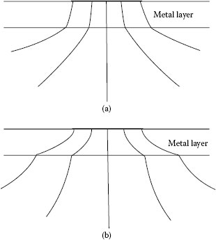
FIGURE 1.19
Current distribution in a metal surface film under conditions where: (a) The film resistivity is larger than that of the substrate material and the a-spot radius is of the same order of magnitude as the film thickness. (b) The film resistivity is smaller than that of the substrate and the current lines spread out more appreciably within the plating than within the substrate.
where ρ is the resistivity of the substrate material. Since the current also passes through the resistive film of area πa2, thickness d and resistivity ρf, the additional film resistance is approximately ρfd/πa2. To a first approximation and for the case where the film is sufficiently thin, the total resistance Rt then becomes
(1.19a) |
This expression reduces to
(1.19b) |
We recall that Equation 1.19b represents the resistance only of the coated surface. An evaluation of contact resistance as measured by a contact probe requires the addition of the spreading resistance from the probe to this equation. Under conditions where the a-spot radius and the plated layer thickness do not differ greatly, the spreading resistance thus increases approximately linearly with plating thickness. For a sufficiently thick film, the spreading resistance will of course deviate from the above expression and approach the value ρf/4a. Equation 1.19b is useful in pointing out that the effect of constriction resistance is overshadowed by the film resistance whenever the ratio (ρf/ρ)(d/a) is much larger than unity. The validity of this conclusion was verified by computer simulations reported by Nakamura and Minowa [55].
Where the resistivity of the plating material is smaller than that of the substrate, the current lines spread out more appreciably within the plating than within the substrate, as illustrated in Figure 1.19b, and the spreading resistance decreases with increasing film thickness. Here again, the spreading resistance approaches the value ρf/4a, where the a-spot is much smaller than the film thickness. Whether ρf is smaller or larger than the substrate resistivity, the effect of the plating on contact resistance is often evaluated via the ratio
(1.20) |
where Pf{d/a,ρf,ρ} is the “plating factor” and ρeff is the effective resistivity of the plated substrate; and ρeff = ρ for d = 0. The plating factor may be evaluated easily using the algorithm described by Williamson and Greenwood [56]. Figures 1.20 and 1.21 illustrate the calculated dependence of the plating factor on the ratio d/2a respectively for typical cases for which ρf/ρ>1 and ρf/ρ<1 [56]. Note that Pf reaches a limiting value for d/2a ≈ 1 for all the cases illustrated. The spreading resistance of a plated surface is, thus, given as ρeff/4a.
In practice and as indicated earlier, the effect of surface deformation on contact resistance must also be taken into account. If the resistivities of the two rough contacting materials (e.g. the plated surface and a measuring probe) are respectively ρ and ρp, and the effective resistivity of the plated material is ρPf, Equation 1.11 immediately yields the contact resistance as
(1.21) |
where again H is the hardness of the softer metal in the interface. Recall also that Pf becomes a function of the load F since the dimensions of a-spots in the interface are affected by F. Thus, in practice, the contact resistance of an electrical interface in which the surfaces are rough, and in which one of the surfaces carries a conductive metallic film, may decrease with increasing load somewhat differently than as F−1/2.
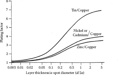
FIGURE 1.20
Dependence of the plating factor on the ratio d/2a for the case of ρf/ρ > 1. (From JBP Williamson and JA Greenwood, Proc Int Conf Elect Cont Electromech Comp, Appendix, Beijing, China, Oxford: Pergamon Press, 1989 [56].)
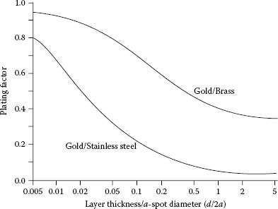
FIGURE 1.21
Dependence of the plating factor on the ratio d/2a for the case of ρf/ρ < 1. (From JBP Williamson and JA Greenwood. Proc Int Conf Elect Cont Electromech Comp, Appendix, Beijing, China, Oxford: Pergamon Press, 1989 [56].)
It is instructive to consider one example of the use of Equation 1.21. Consider a gold probe at room temperature in contact with a load of 0.1 kgf on a copper surface plated with a tin layer of thickness 10 μm. From Table 24.1 (see Chapter 24), the hardness of gold (30 kg mm−2) is much larger than that of tin (4 kg mm−2), so that the hardness value H used in Equation 1.21 is that of tin. From Equation 1.10, the area of metal-to-metal contact is calculated as F/H or 0.1/4 = 0.025 mm2, thus yielding an average contact radius of √0.025/π=0.089 mm or 89 μm. The ratio of layer thickness to average diameter of contact spot is, thus, 10/178 = 0.06, which yields a plating factor Pf of 2 from Figure 1.20. Using ρp = 2.3 × 10⁻⁵ Ωmm for gold and ρ = 1.75 × 10⁻⁵ Ωmm for copper, the contact resistance is given as
Rt=2.3×10⁻⁵+1.75×10−5×22{π44×0.1}1/2=1.63×10−4Ω
Consider now the effect of a contaminant film on contact resistance. Since the resistivity ρcont of contaminant materials is generally much larger than that of metals, the effect on contact resistance is evaluated using the procedure that led to Equation 1.19a. This procedure yields a film resistance of ρcontdcont/πa2, where dcont is the thickness of the contaminant film. Since the contact area is given as F/H(i.e., πa2=F/H), the total contact resistance is now given as
(1.22) |
Expression 1.22 is used in practice to interpret contact resistance data measured from plated surfaces. In engineering evaluations of metal coatings for connectors, and in the ensuing interpretation of contact resistance data in terms of Equation 1.22, the electrical contact properties are generally measured by loading a metal probe onto the coated surface and recording the electrical resistance as a function of the applied force. The probe material is often pure gold with a smooth hemispherical end with a radius of 1.6 mm. A dependence of contact resistance on load as F−1 is usually taken as evidence (from Equation 1.22) of the presence of contaminant material on the surface [57,58]. Details of the metal probe and measuring procedure are given in the ASTM Standard Practice [59]. We now provide examples of such measurements of contact resistance.
Figure 1.22 shows a plot of contact resistance as a function of contact force for tips of five different gold probes pressed against a gold target [60]. Four of the probes were characterized by a spherical contact surface with a radius respectively of 3.2 mm, 1.6 mm, 1.2 mm, 0.9 mm; the fifth was prepared by machining the end of a gold rod 3.18 mm in diameter to a 60° cone with a sharply pointed tip. The measured contact resistance is very close to the values predicted on the basis of Equation 1.22 in the absence of a contaminant film (i.e., dcont = 0). The one exception to the predicted behavior is for the conical tip. In this case, the investigators found that the larger resistance measured with this tip stemmed from a larger bulk resistance [60]. When this resistance component is subtracted from the measured contact resistance, the curve obtained using the conical tip coincides with the curves yielded by the others. Note that the curves of Figure 1.22 are essentially independent of the radius of the gold probe and that contact resistance depends only on the applied force. This is indeed as predicted by Equation 1.22 with dcont = 0. Thus, the area of metal-to-metal contact in the electrical interface is independent of the details of probe geometry and depends only on hardness.
Figure 1.23 shows the results of contact resistance measurements on freshly polished copper using the five gold tips referred to in Figure 1.22. There is a significant difference between these results and those of Figure 1.22 for gold-gold contacts. The slope of the initial parts of the curves, to a load of 20 gf, is approximately −1 and the contact resistance is generally larger than obtained from gold–gold. The initial inverse proportionality to load F suggests that the contact behavior is described by Equation 1.22 where dcont ≠ 0, that is, in the presence of a contaminant film of relatively large resistivity such as an oxide film. The investigators found a good fit to Equation 1.22 using a value of 2.75 × 10⁻¹⁴ Ω m2 for ρcontdcont. Note again the curves of Figure 1.23 are essentially independent of probe geometry as predicted by Equation 1.22. The observations of Figures 1.22 and 1.23 support the premise that the area of metal-to-metal contact is determined only by plastic deformation (hardness) of the contacting surfaces. Additional examples of the type of contact resistance measurements depicted in Figures 1.22 and 1.23 are easily accessible in the literature on contact-resistance. These are described in [61,62].
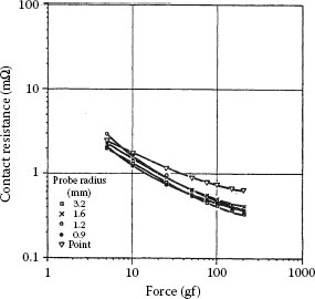
FIGURE 1.22
Contact resistance versus applied force for gold probes of various tip radius: Clean gold-to-gold. (From MR Pinnel and KF Bradford, Proc 28th Elect Comp Conf, Anaheim, CA 129, 1978 [60].)
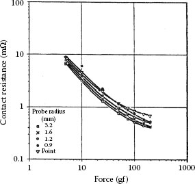
FIGURE 1.23
Contact resistance versus applied force: Clean gold on freshly polished copper. (From MR Pinnel and KF Bradford, Proc 28th Elect Comp Conf, Anaheim, CA 129, 1978 [60].)
1.3.3 Growth of Intermetallic Layers
The formation of intermetallic compounds arises from the interdiffusion of materials across a bimetallic interface. In electrical contacts, this interdiffusion occurs when the electrical interface is operated in a high-temperature environment or when sufficient electric current is passed through the contact to raise the temperature of the a-spot to well above the ambient temperature. The relationship between a-spot temperature and voltage drop across the contact will be addressed in Section 1.4.
Recent decades have witnessed a surge of interest in interdiffusion phenomena at bulk and thin-film bimetallic interfaces due respectively to the increased use of bimetallic welds in a variety of applications [63,64,65,66,67,68,69,70,71,72] and to the ubiquitous use of multi–thin-film structures in microelectronic devices [73]. Bulk joints are made using a variety of techniques ranging from pressure and friction welding to flash and explosive welding. In electrical applications, frequent electrical surges or operation of a device at relatively elevated temperatures may generate conditions favorable to formation of intermetallic layers in bimetallic electrical contacts, since interdiffusion is thermally activated. The formation of these layers is generally deleterious to the electrical stability and mechanical integrity of a bimetallic joint because intermetallic phases are usually characterized by high electrical resistivity and low mechanical strength [63,64,65,66,67,68,69,70,71,72]. For example, experimental evidence indicates the growth of an intermetallic layer considerably weakens the strength of an aluminum–copper joint [74]. The subject of formation of intermetallics also draws considerable attention in the microelectronics industry because of the intimate relationship of this phenomenon to the reliability of bimetallic thin-film contacts in microelectronic devices (see for example references [75,76,77]). This section reviews the intermetallic growth at interfaces of bulk electrical contacts of common interest such as aluminum–copper, aluminum–brass and plated layers on brass and phosphor bronze. For illustrative purposes, data obtained from aluminum–brass joints [70] will be used.
Figure 1.24 shows micrographs of two aluminum–brass interfaces obtained by scanning electron microscopy (SEM) after the joints had been heated in a furnace respectively for 765 hours at 250°C and for 6 hours at 400°C [70]. The brass consisted of wt% Cu70Zn30. The intermetallic layers consist of four distinctive bands and the total interdiffusion layer thicknesses differ significantly due largely to the large difference in the temperature of exposure. Figure 1.25 shows the growth of the layers measured at temperatures of 250°C–240°C. For each case, note that the thickness x of the separate layers grows according to the relation
(1.23) |
where k is the interdiffusion rate constant at the selected temperature and t is the interdiffusion time. There is a clear proportionality of layer thickness to t1/2 for all temperatures. At first glance, this observation is surprising since atoms that diffuse from one end of the bimetallic joint to the other do not cross the same number of interlayer boundaries and travel ever increasing distances as the thickness x increases. However, the work of Gosele and Tu [78] indicates that this observation is consistent with expected growth of the interdiffusion layer if diffusion of atoms through intermetallic layers is considerably slower than diffusion across interlayer boundaries. The activation energy characterizing the growth of each intermetallic layer in aluminum–brass interfaces was determined in [70] on the assumption that the dependence of k on temperature is expressed as
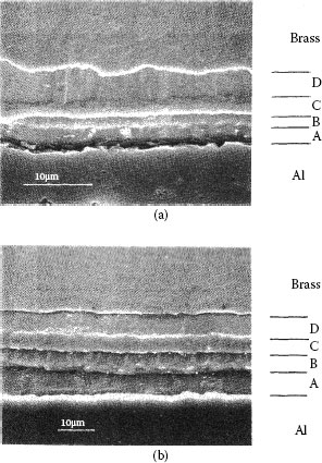
FIGURE 1.24
Micrographs of two aluminum–brass interfaces obtained by scanning electron microscopy (SEM) after the joints had been heated in a furnace respectively for (a) 765 hours at 250°C and (b) 6 hours at 400°C. (From RS Timsit, Acta Met 33: 97, 1985 [70].)
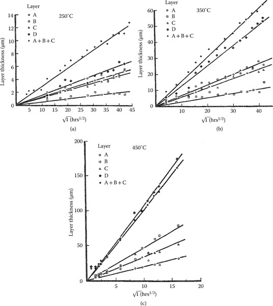
FIGURE 1.25
Growth rate of intermetallic layers at temperatures of 250°C–450°C at aluminum–brass interfaces. (From RS Timsit, Acta Met 33: 97, 1985 [70].)
(1.24) |
where k0 is a constant, Q is the activation energy, R is the universal gas constant (1.987 cal K−1) and T is the absolute temperature. The results of the analysis are shown in Figure 1.26 and are summarized in Table 1.4. It was found that intermetallic growth could generally not be described satisfactorily by a single activation energy over the entire temperature range but that an adequate description was possible by considering the data from the temperature regions 150°C–300°C and 350°C–450°C separately. As shown in Table 1.4, the activation energies determined for temperatures lower than approximately 300°C are considerably smaller than those obtained for the more elevated temperatures. The lower activation energies may be indicative of intermetallic growth by mechanisms such as grain boundary diffusion or dissociated dislocation [79]. The activation energies above 300°C are characteristic of bulk diffusion. Similar observations of changes in activation energies over the two temperature regions were made [72] in an investigation of interdiffusion in bulk aluminum–copper diffusion couples similar to that described in [70]. As indicated in Table 1.4, the values of Q in the temperature ranges 150°C–300°C and 350°C–450°C for the diffusion bands (A + B + C) at aluminum–brass interfaces are nearly identical to those measured in aluminum–copper bulk diffusion couples [72]. The chemical compositions of the layers formed at various temperatures at aluminum–brass interfaces are shown in Figure 1.27. Note the compositions do not vary appreciably as the temperature increases. A summary of the composition and crystal structure of the interdiffusion layers is also given in Table 1.4.
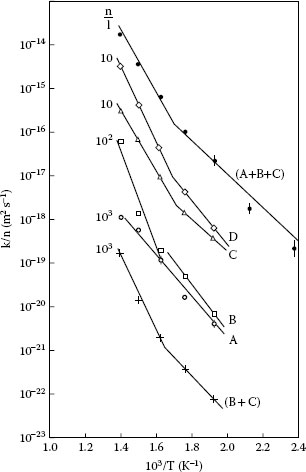
FIGURE 1.26
Arrhenius plots of the rate constants for growth of the various interdiffusion bands at an aluminum–brass interface. (From RS Timsit, Acta Met 33: 97, 1985 [70].)
TABLE 1.4
Summary of Composition, Crystal Structure, and Growth Rates of Intermetallic Compounds Formed at Aluminum–Brass, Aluminum–Copper, Plating–Brass, and Plating–Phosphor-Bronze Interfaces
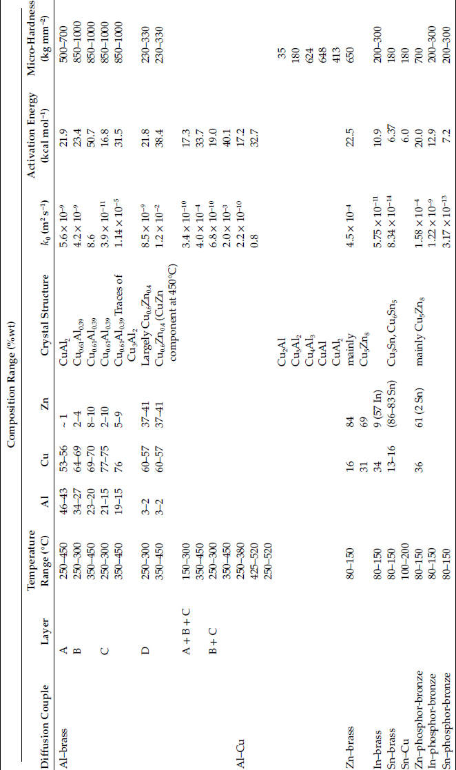
Source: RS Timsit, Acta Met 33: 97, 1985 [70]; RS Timsit, IEEE Trans Comp Hyb Manuf Tech CHMT-9: 106, 1986 [71]; M. Braunovic and N. Alexandrov, IEEE Trans CompPack Manuf Tech CHMT-A17: 78, 1994 [72]. With permission.

FIGURE 1.27
Chemical composition of intermetallic layers formed at aluminum–brass interfaces at various temperatures. Note that the compositions do not vary appreciably as the temperature increases. (From RS Timsit, Acta Met 33: 97, 1985 [70].)
It was mentioned that the brittleness and related properties of intermetallic layers can lead to a weakening of the interface in which the layers grow. The data of Figure 1.28 illustrate this effect for an aluminum–copper interface where the peeling force between the two mating surfaces was measured after various time intervals for interdiffusion [74]. The strength of the interface decreased precipitously with increasing thickness of the intermetallic layer once the width of the layer exceeded approximately 2 μm.
Many electrical connectors produced from copper–base alloys use electroplated layers such as tin, indium or even zinc to improve stability of the contact or mitigate attack by corrosion. The choice of plating material is often based on the ability of the material to form a relatively soft coating which flows under the action of contact stresses to form a long unbroken electrical interface. An important issue which must be addressed is the formation of intermetallics at electrical interfaces with electroplates at the recommended operating temperatures of the connectors.
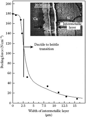
FIGURE 1.28
Variation of peeling force with intermetallic width. (From M Abbasi et al., J Alloy Comp 319: 233, 2001 [74].)
Tin, indium and zinc interdiffuse with brass (wt% Cu70Zn30) and phosphor bronze (wt% Cu95Sn5) to form clearly defined diffusion layers. The measured characteristics are summarized in Table 1.4. Illustrative examples of the interdiffusion bands formed between brass and zinc, indium and tin layers are illustrated respectively in Figures 1.29 through 1.31 [71]. The band formed with zinc consists of two layers labeled A′ and B′ in Figure 1.29. The composition of the layers is listed in Table 1.4. The Knoop microhardness of the intermetallic layer B′ was measured as 650 kg mm−2. The interdiffusion layer formed with indium also consists of two layers labeled A″ and B″ in Figure 1.30. Layer B″ consists of an intermetallic compound whose composition is given in Table 1.4. The Knoop micro-hardness is of the order of 300 kg mm−2. The interdiffusion band produced with tin exhibited widely spaced nucleation regions as illustrated in Figure 1.31. The Knoop microhardness of the layer whose composition is given in Table 1.4 is ~ 180 kg mm−2. Examples of growth curves for interdiffusion bands produced on brass and phosphor bronze are shown respectively in Figures 1.32 and 1.33. Note that the growth rates in brass and phosphor bronze are similar. The width of the interdiffusion bands is found to increase with time in accordance with Equations 1.23 and 1.24. The activation energies for the two substrates are listed in Table 1.4.
The growth of intermetallic layers in an electrical interface produces material gradients characterized by large changes in microhardness. These abrupt variations in hardness cause mechanical strains that may lead to mechanical fracture of the interface, particularly during thermal excursions in the service life of the connection. For these reasons and as already illustrated in Figure 1.28 [63,64,65,74], intermetallic growth may, thus, be highly deleterious to the mechanical and electrical integrity of an interface. There is an additional effect due to intermetallics. Since intermetallics are characterized by relatively large electrical resistivities, their growth within a-spots increases the electrical contact resistance. The experimental data presented below represent the few direct illustrations of this effect in the published literature [80] and is worth describing in detail.
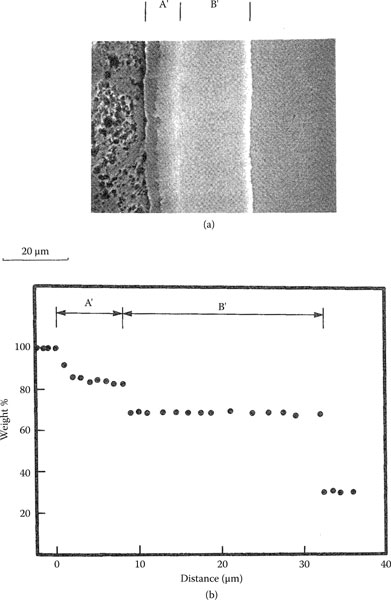
FIGURE 1.29
(a) Example of interdiffusion band formed at a brass–zinc interface (b) Zn concentration in interdiffusion bands shown in (a); the composition balance consists of Cu. (From RS Timsit, IEEE Trans Comp Hyb Manuf Tech CHMT-9: 106, 1986 [71].)
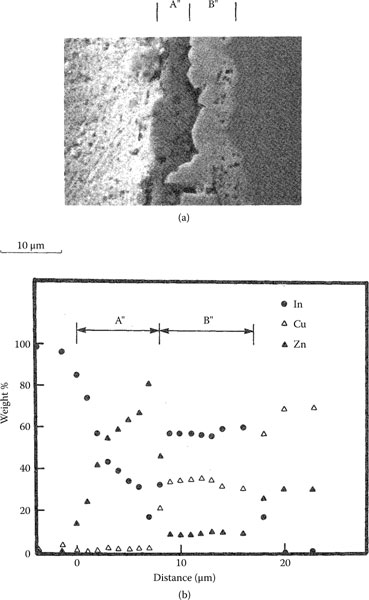
FIGURE 1.30
(a) Example of interdiffusion band formed at a brass–indium interface (b) Chemical composition of interdiffusion layer in (a). (From RS Timsit, IEEE Trans Comp Hyb Manuf Tech CHMT-9: 106, 1986 [71].)
Using Equation 1.1, it may be shown that the cold resistance Rcl of a layered contact spot, such as the aluminum–brass a-spot illustrated in the inset of Figure 1.34, is given as [80]
(1.25) |
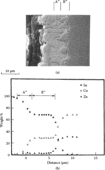
FIGURE 1.31
(a) Example of interdiffusion band formed at a brass–tin interface (b) Chemical composition of interdiffusion layer in (a). (From RS Timsit, IEEE Trans Comp Hyb Manuf Tech CHMT-9: 106, 1986 [71].)
where ρAl, ρBr and ρint are respectively the resistivities of aluminum, brass and an intermetallic layer formed in the contact; a0 is the true contact radius. In the derivation of Equation 1.25, the temperature is assumed to be uniform within the contact. Since ρint>ρAl,ρBr [81], the contact resistance given by Equation 1.25 is larger than the resistance without the intermetallic layer, that is, when δ = 0. An “equivalent” radius of the contact may then be defined as
aeq=ρAl+ρBr4Rcl
representing the radius of a circular a-spot formed between aluminum and brass in which the constriction resistance has the value given by Rcl from Equation 1.25, but without intermetallics. The equivalent radius aeq is clearly smaller than the true radius a0. From Equation 1.25, it follows that
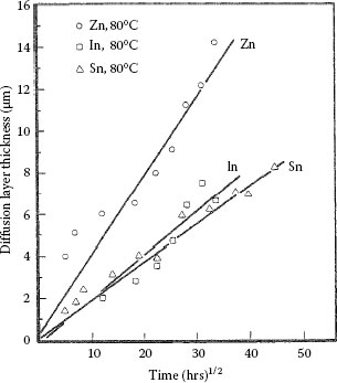
FIGURE 1.32
Growth of interdiffusion bands (Aʹ + Bʹ), Bʺ, and Bʹʺ’ generated respectively with Zn, ln, and Sn layers on brass at 80°C. (From RS Timsit, IEEE Trans Comp Hyb Manuf Tech CHMT-9: 106, 1986 [71].)
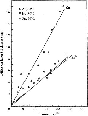
FIGURE 1.33
Growth of interdiffusion bands (Aʹ + Bʹ), Bʹ, and Bʹʺ generated respectively with Zn, ln, and Sn layers on phosphor bronze at 80°C. (From RS Timsit, IEEE Trans Comp Hyb Manuf Tech CHMT-9: 106, 1986 [71].)
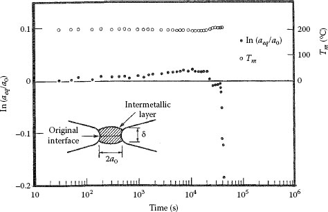
FIGURE 1.34
Effect of intermetallic growth on the equivalent contact radius aeq; a0 = 0.34 μm in an aluminum–brass contact. (From RS Timsit, Can Elect Assoc Rep 76–19, 1976 [80].)
(1.26) |
where
r=2ρintρAl+ρBr
From Equation 1.26, the thickness δ1/2 of intermetallics required to decrease the equivalent radius aeq from the initial value a0 to a0/2 is found to be
δ1/2a0=2tan{π2(r−1)}
Table 1.5 lists the values of δ1/2/a0 for various values of the ratio r. Since ρAl=2.6×10⁻⁸Ωm, ρBr=6.3×10⁻⁸Ωm and ρint∼2×10⁻⁷Ωm [79] at room temperature, r has the value of approximately 4 and should be reasonably independent of temperature. For aluminum–brass contacts, Table 1.5 indicates that δ1/2/a0 takes the value of 1.2 for r = 4. Thus, the equivalent radius aeq should drop to one-half the value of a0 when
δ1/2∼a0
that is, when the thickness of the intermetallic layer is approximately equal to the a-spot radius.
TABLE 1.5
Dependence of δ1/2/a0 on Ratio r
r |
δ1/2/a0 |
2.5 |
3.5 |
3 |
2.0 |
4 |
1.2 |
5 |
0.8 |
6 |
0.7 |
7 |
0.5 |
The experimental data of Figure 1.34 illustrate the effect of intermetallic growth on the contact resistance of a constriction formed between aluminum and brass [80]. The data were obtained by measuring the contact resistance between two contacting hemispherical surfaces of aluminum and brass, cleaned in vacuum and pressed against one another under a sufficiently low mechanical load to produce one electrical contact spot of initial radius a0= 0.34 μm [80]. The contact spot was heated at a near-constant temperature of 198°C for a number of hours to grow intermetallics within the a-spot. The “cold” resistance was evaluated as a function of time from measurements of drop in voltage across the contact and of bulk temperature (this evaluation procedure is described in Section 1.4). The “equivalent” radius aeq plotted in Figure 1.34 was found to remain constant for approximately 4 × 10⁴ s, after which it decreased very rapidly. We now show that this time interval for a significant increase in contact resistance (or decrease in aeq) due to intermetallics is consistent with the growth rates of intermetallics expected on the basis of the information in Table 1.4.
From Table 1.4, the intermetallic layer of high resistivity in the aluminum–brass interface is the (A + B + C) band. Since this band grows in a parabola with the rate constant
(1.27) |
according to Table 1.4, at the contact temperature of 198°C (471 K) corresponding to Figure 1.34, the rate constant k has the value of 3.4 × 10⁻¹⁰exp(−17,300/(1.987 × 471)) or 3.19 × 10⁻¹⁸ m2 s−1. From Equation 1.23 the time required for the intermetallic layer to attain the thickness δ1/2 at 198°C is given as [61/2]2/k. Since δ1/2 = a0 = 0.34 μm, this time interval has the value [0.34 × 10⁻⁶]2/3.19 × 10−18 or 3.7 × 10⁴s. This is in excellent agreement with the time interval [4.2 × 10⁴s] shown in Figure 1.34 when the equivalent radius aeq decreased by a factor of two. Figure 1.34 illustrates vividly the effect of intermetallic growth on contact resistance. In practice, the operating temperature of a bimetallic electrical contact must be maintained low to preclude this type of growth. However, because the activation energies associated with interdiffusion of plated layers with brass are relatively small, interdiffusion occurs relatively rapidly even at room temperature as illustrated in Table 1.6.
Table 1.6 lists the thickness of the intermetallics formed by Zn, ln, and Sn layers with brass both at room temperature and at 55°C (the maximum recommended operating temperature of some switching devices) for various time intervals. Clearly, all the platings interdiffuse relatively rapidly to generate a surface layer harder than the original brass even at room temperature. Similar conclusions have been made regarding the effect of intermetallic growth on the contact resistance properties of tin-plated copper [82]. As shown in Table 1.4, the activation energy for intermetallic growth in tin–copper interfaces is almost identical to that measured in the tin–brass system. These results suggest that any electrical junction made with tin-plated copper or brass is potentially unstable even if the contact is relatively cool. The shelf storage lifetime of devices coated with any of the plating materials listed in Table 1.6 is clearly severely limited. Of greatest concern must be devices coated with zinc since the hardness of the interdiffusion layer is very large in this case. The generation of a hard surface layer would not only act to reduce the area of electrical contact but would also produce a brittle interface, which is deleterious to the mechanical stability of the junction. The growth of a hard surface layer may explain in part the unreliability of zinc-plated connector plates in household electrical wiring devices [83].
TABLE 1.6
Thickness of Interdiffusion Layers Produced by Zinc, Indium, and Tin Deposits on Brass
|
|
Interdiffusion |
Layer |
Thickness (μm) |
Time Interval |
T (°C) |
Zn |
ln |
Sn |
1 month |
20 |
0.14 |
1.0 |
1.9 |
1 year |
20 |
0.48 |
3.5 |
6.7 |
1 month |
55 |
3.4 |
2.8 |
3.5 |
1 year |
55 |
11.8 |
9.8 |
12.1 |
It is clear from the above considerations that intermetallic growth may be highly deleterious to the reliability of electrical contacts. Although the illustrative examples of this section have focused on interfaces involving copper-based alloys, the effects are not restricted to these types of interfaces and apply generally to a wide number of bimetallic couples. The literature on the effects of intermetallic layers on the mechanical integrity of an electrical interface is vast and has expanded significantly in recent years. This is due, in large part, to the adoption of lead-free solders and lead-free tin coatings on electrical contact surfaces in the electronics industry and the need to characterize the effect of intermetallic growth on the mechanical strength of soldered electrical joints. Intermetallic growth also has deleterious effect on the strength of ultrasonic bonded electrical interfaces in microchips. A great deal of the literature on intermetallic growth focuses on electrical contact materials such as copper, copper-based alloys, tin, nickel, aluminum, and gold. This is addressed in detail in references [84,85,86].
Interdiffusion in electrical interfaces comprising copper-based alloys is usually mitigated through the use of a diffusion barrier such as nickel. The effectiveness of the barrier depends on the microstructure as well as the thickness of the layer. A layer of nickel about 1 μm thick inhibits interdiffusion in a copper–tin contact. Interdiffusion between the tin and nickel still occurs but is characterized by slow intermetallic growth over a wide temperature range, generally to form Ni3Sn4 [87,88,89]. The use of a nickel–iron-plated layer to inhibit interdiffusion of Sn with copper has also been recommended [90]. Although electroplated and electroless nickel have been the interdiffusion barrier materials of choice in connector applications, efforts are being made to develop other materials such as nanocrystalline nickel–tungsten alloys to further enhance resistance to not only interdiffusion but also corrosion and mechanical wear of overplates [91]. Some of the intrinsically materials-related requirements for thin films to act as effective diffusion barriers have been reviewed by Nicolet [92].These requirements are likely valid for thick coatings such as electroplates.
The selection of an appropriate diffusion barrier for surfaces in an electrical contact subjected to a mechanical contact load must satisfy another major criterion in addition to that of mitigating interdiffusion. The barrier layer must also be characterized by mechanical properties that are compatible with those of the substrate material to preserve physical integrity. For example, although a nickel layer mitigates tin diffusion into aluminum [93], the softness of aluminum relative to nickel may lead to fracturing of the latter under the action of a sufficiently large contact load. Cracking of the nickel leads to penetration of tin into the aluminum and may also lead to severe galvanic corrosion between tin, nickel and aluminum.
Because diffusion barriers add to fabrication cost, they are often not used in connectors if it is assessed that the operating temperature of the connector shall always remain relatively low.
1.3.4 Possible Effect of Electromigration on Intermetallic Growth Rates
The data on interdiffusion described in Section 1.3.3 were obtained from thermally annealed specimens. If these data are to be extrapolated reliably to predict intermetallic growth in practical electrical contacts, it must be established that this growth is unaffected by the presence of an electric current of high density, that is, by the effects of electromigration. Because the open literature on electromigration in bulk electrical contacts deals largely with aluminum–brass, aluminum–copper and aluminum–aluminum interfaces [72,80,94,95], in this section, we will focus on these types of electrical contacts in examining electromigration.
Consider some fundamental principles of electromigration. Theoretically, the passage of a direct electric current in a metal specimen in which thermal diffusion occurs does not affect either impurity or self-diffusion rates in the metal. The action of the electric current is only to shift the zone of material gradients which results from diffusion [96]. Although the effect of this shift on the mechanical integrity of the interface is unclear, the effect would be expected to be small if the shift were much smaller than the width of the diffusion bands. The direction of this shift depends on the direction of the electric current and its magnitude y is given as [96]
y=vt
where v is the velocity with which the shift occurs and t is the time, with
v=eZ*DρjkT
In the above expression, e is the magnitude of the electronic charge, Z* and D are respectively the effective charge number and the diffusion coefficient of the diffusing species, ρ is the electrical resistivity of the diffusive host, j is the electric current density, k is Boltzmann’s constant and T is the absolute temperature. Consider now the magnitude of the shift expected in the location of the diffusion band at an aluminum–brass interface (discussed in Section 1.3.3 above) due to the action of an electric current. Whether the diffusing species is aluminum, copper, or zinc, the diffusion coefficient D in the above expression cannot be larger than the rate constant for the growth of the intermetallic layer (A + B + C) given in Equation 1.27. Taking D = rate constant as an upper bound, ρ ∼2×10⁻⁷Ωm (for the intermetallic) [81] and Z* ~10 [96] yields
v=1.0×10⁻²²j ms−1
at a temperature of 200°C (say an upper bound for an operating contact). Since the current density in a functional bulk contact seldom exceeds 108 Am−2, the shift cannot exceed approximately 36 nm after 1000 hours of operation. This is totally negligible in comparison with the thickness of the intermetallic band grown thermally under these conditions. There is, thus, no theoretical basis for expecting an effect of electromigration on the performance of aluminum–brass electrical interfaces operating within this limit.
In order to determine (1) Whether this conjecture regarding the effect of electric current is indeed correct, and (2) Whether the values of the parameters used to evaluate the velocity v defined above indeed provide an upper bound for the shift, experiments were performed to measure both the interdiffusion bandwidth and the band shift in diffusion couples heated by passing an electric current [80]. In the experiments, aluminium–brass couples were Joule-heated with a current density of 0.1 – 108−1 × 10⁸ Am−2 at the electrical interface, to a temperature of the order of 300°C to grow intermetallic layers reasonably quickly. The experimental set-up is shown schematically in Figure 1.35. The diffusion couples were formed by roll-bonding sheets of aluminum and brass to obtain a composite material consisting of aluminium–brass–aluminum [80]. A direct electric current was passed through the specimen as shown in the diagram so that two diffusion interfaces could be exposed to the electrical flow simultaneously. A thermocouple was located on one side of the specimen to measure the temperature resulting from Joule-heating.
Because of the difference in the direction of electrical flow across each aluminum–brass interface in the specimen, any electrically induced shift in the diffusion band should occur into the aluminum in one interface and into the brass in the other. The shift was, thus, measured by determining the average difference between (1) The mean distance between one edge of the diffusion band and the original aluminum–brass interface on one side and (2) The mean distance between the corresponding boundaries on the opposite side. Typical results on bandwidths and bandshifts are shown in Table 1.7.
The measured bandwidths were always a little larger than those calculated from the rate constant defined in Table 1.4 on the basis of the mean temperature recorded on the electrical couple during the experiment. However, since the measured temperature was likely to be lower than the temperature of the interface, the differences between measured and calculated band thickness cannot be unequivocally attributed to the presence of electrical flow. This point is illustrated in column 7 of Table 1.7, which lists the temperature (Tcalc) required to bring the calculated and measured band thickness into agreement in each run of the experiment. The deviation between the required interface temperature and that measured on the specimen skin is, indeed, not large with the exception of the last entry. It is emphasized, however, that the large deviation in this last case is not inconsistent with the large temperature gradient expected within the specimen under the action of the large electric current (200 A) used in the experiment. Hence, within the uncertainties of these experiments, the rate of intermetallic growth is consistent with that predicted from Table 1.4 and appears unaffected by the presence of electric current. This is in keeping with the predictions of conventional theory of electromigration. It is the present author’s opinion that other investigations claiming observations of significant electromigration components to interdiffusion suffer similar uncertainties [72].
The bandshift arising from possible electromigration (column 9 of Table 1.7) is negligible and consistent with the small shifts predicted theoretically (column 10). These observations, along with the insensitivity of growth kinetics to electric current, lend credence to the estimates obtained above that electromigration in aluminum–brass contacts is negligible under conditions of interest in practice (T – 200°C, j ~ 108 Am−2).
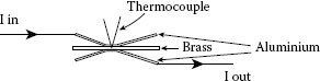
FIGURE 1.35
Experimental setup for the investigation of electromigration at aluminum–brass interfaces. (From RS Timsit, Can Elect Assoc Rep 76–19, 1976 [80].)
TABLE 1.7
Results of Tests for Effects of Electromigration on Intermetallic Growth in Aluminum-Brass Contacts
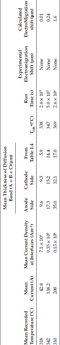
a Tcalc is the temperature required to bring the calculated band thickness into agreement with the experimental value.
In summary, intermetallic growth at aluminum–brass interfaces under conditions of interest in bulk electrical contacts is sensitive to temperature and is not expected to be affected significantly by the presence of an electric current. Although the illustrative examples described above focused on aluminum/brass interfaces, the author’s experience indicates that this conclusion applies to a wide range of bulk electrical interfaces of practical interest such as copper–brass, copper–tin-plated brass, and so on at current densities on the order of 0.1 × 10⁸−1 × 10⁸ Am−2. However, investigations of interdiffusion at copper–tin interfaces at temperatures approaching the melting point of tin have pointed to an effect of electromigration on Cu–Sn intermetallic growth rates at current densities of ~ 4 × 10⁸ A m−2 [97]. Thus, it is possible that electromigration effects on intermetallic growth were not detected in aluminum–brass interfaces due to the insufficient current density and low temperature (i.e., much lower than the melting point of aluminum or brass).
1.3.5 Electrically Insulating or Weakly Conducting Films
Electrically insulating or weakly conducting surface films usually stem from the formation of oxide or corrosion products on contact surfaces. Often, these types of films are mechanically brittle, for example, Al2O3 films on aluminum, and electrical contact is established only after the films are fractured and metal-to-metal contact spots are formed by metal extrusion through cracks in the insulating layers. Under these conditions, the shapes of a-spots, and thus the constriction resistance, are determined by the shapes of cracks and the fracture mode of the insulating films [98]. Figure 1.36 shows the transmission electron micrograph of an Al2O3 film removed from an AA1350 aluminum surface after formation of an electrical contact. The contact consisted of two smooth hemispherical aluminum surfaces [80]. The electrical contact spots were formed by metal flow through the narrow fissures evident in the film.
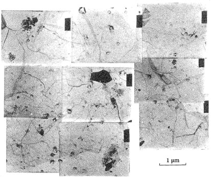
FIGURE 1.36
Transmission electron micrograph of an Al2O3 film removed from an aluminum surface in a compression electrical contact. The dark areas correspond to fracture regions in the film. (From RS Timsit, Can Elect Assoc Rep 76–19, 1976 [80].)
The contact resistance in the electrical interface corresponding to Figure 1.36, measured in air as a function of the applied load, is illustrated in Figure 1.37a [80,99]. Note the threshold load of approximately 1 N to fracture the insulative oxide layers in the interface. Figure 1.37b shows the behavior of the identical contact interface formed in ultra-high vacuum where the oxide films on the two contacting aluminum surfaces had first been removed by ion-beam etching [80,99]. In contrast to the data of Figure 1.37a, the absence of oxide not only leads to instant electrical contact when the surfaces touch but also leads to cold welding of the clean metal surfaces, evidenced by the generation of a significant adhesion force on removal of the contact load. A comparison of the curves of Figure 1.37 provides clear evidence of the deleterious effect that oxide or other surface films with high resistivity can have on the generation of a reliable electrical contact. In this section, we shall review the electrical properties of a few metal oxides, such as copper and aluminum oxides, before discussing the full effect of surface oxide films on electrical contact resistance.
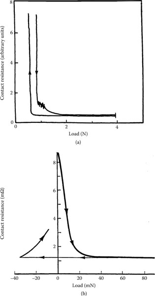
FIGURE 1.37
Contact resistance in an aluminum/aluminum contact with: (a) Oxide films present on the contact surfaces (b) Oxide films removed from the contact surfaces. (From RS Timsit, IEEE Trans Comp Hyb Manuf Tech 3: 71, 1980 [99].)
1.3.5.1 Growth Rate and Electrical Resistivity of Oxides of Selected Contact Materials
The data available on the oxidation of copper at temperatures between 100°C and 200°C [100,101] suggests that the law of oxidation rate is relatively independent of the oxygen pressure and is either inverse logarithmic, direct logarithmic or of the form
(1.28) |
where d is the oxide film thickness, n ≤ 3, k″ is a constant, and t is the time. Assuming a cubic rate law, the data of Campbell and Thomas [102] suggest that at a temperature of 100°C, Equation 1.28 should take the form
d3=0.86t
where d is in nanometers and t is in seconds. Thus, the growth rate is relatively rapid and it requires approximately 9 seconds for a copper oxide film to grow to a thickness of 2 nm at a temperature of 100°C. The electrical conductivity of copper oxide is highly dependent on the nature of the oxide formed that is, cupric (CuO), cuprous (Cu2O) or the other (CuO0.67) oxide phase. Cupric oxide is a relatively better electrical conductor than the other two oxides, with a specific resistance of 1–10 Ωm [103]. Cuprous oxide (and presumably CuO0 67), on the other hand, is a p-type semiconductor with a specific resistance that is highly sensitive to temperature. The experimental data of Anderson and Greenwood [104] indicate that the specific resistance of cuprous oxide may be written as
(1.29) |
where ρCu2O and kT are expressed in Ωm and eV respectively. At a temperature of 100°C, it is found that ρCu2O=4.5×10³ Ωm, a value considerably larger than for cupric oxide.
The dependence of the composition of a copper oxide film on oxygen pressure and temperature may be understood from Figure 1.38 reproduced from the work of Honjo [105,106]. The curves delineate the regions in which electron diffraction studies of oxide films revealed either Cu or Cu2O as the outermost oxide in the film. Thus, below approximately 200°C, no cupric oxide is formed on the oxide surface in open air. Other work [100,107,108] has indicated that little, if any, CuO is present within a copper oxide film grown below 200°C either in air or oxygen at low-to-atmospheric pressures. The electrical resistance, Rf of a copper oxide film at 100°C may thus be calculated as
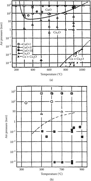
FIGURE 1.38
Pressure–temperature diagram for copper oxides formed by oxidation in air: (a) Pure copper, where three different CuO phases were identified as I, II and III by electron diffraction (b) wt% Cu93Ni7 alloy, where the points are labeled according to the oxide phases identified in (a). The shaded squares correspond to unidentified phases of oxides of copper or nickel. (From G. Honjo, J Phy Soc Japan 4: 330, 1949 [105]; G Honjo, J Phy Soc Japan 8: 113, 1953 [106].)
(1.30) |
where d is the film thickness and A is the surface area of the oxide film.
There are two main oxides of tin: Stannic oxide (SnO2) and Stannous oxide (SnO). The existence of these two oxides reflects the dual valency of tin, with oxidation states of 2+ and 4+. Figure 1.39 shows the Sn–O phase diagram for atmospheric pressure conditions [109,110]. This diagram indicates the presence of an intermediate tin oxide phase between SnO and SnO2 at elevated temperatures. Sn3O4 is often given for its composition but Sn2O3 has also been considered. Stannic oxide is the thermodynamically most stable form of tin oxide. Stannic oxide is an n-type semiconductor and has been used widely in thin-film form as transparent electrode. The electrical resistivity of SnO2 at room temperature varies greatly, from about 102 Ωm for well-prepared bulk oxide material [111] to about 4 × 10⁴ Ωm for oxide layers grown on tin. Because SnO2 is a semiconductor, the conductivity of the oxide rises rapidly with increasing temperature, especially at temperatures higher than approximately 750°C [111].
In a series of investigations, Tamai and coworkers characterized the growth rate and the composition of tin oxide surface films grown in air after electrodeposition of tin layers on a copper–nickel substrate [112,113,114]. Oxide growth rates were measured at temperatures ranging from 25°C to 150°C. Contact resistance properties were also measured. Figure 1.40 shows the oxide growth data at 25°C, indicating a relatively rapid linear oxide growth for the first five hours of exposure of the tin to laboratory air [113]. Following this initial phase of oxidation, the rate eventually decreased to a growth law characterized by n ~ 4 in Equation 1.28. Similar observations were made at the higher temperatures, thus indicating only a small effect of temperature on oxide growth rates up to 150°C [113]. Chemical analyses of the oxide using surface analytical techniques showed that the initial oxide film formed at a temperature lower than 120°C consisted of a mixture of crystalline and possibly amorphous SnO, as well as a mixture of SnO2 and Sn3O4. The presence of these oxide forms is consistent with the Sn–O phase diagram of Figure 1.39. Oxide grown at temperatures higher than 120°C (i.e., higher than the recrystallization temperature of tin) was found to consist largely of crystalline SnO2.
FIGURE 1.39
Sn–O phase diagram. (From M Batzill and U Diebold, Prog Surf Sci 79: 47, 2005 [109]; U Kuxmann and R Dobner, Metallwissenschaft und Technik 34: 821, 1980 [110].)
FIGURE 1.40
Growth rate of tin oxide in an indoor environment at 25°C and 75% RH. (From Y Nabeta et al., Proc 55th Holm Conf Elect Cont, Vancouver, BC, Canada, 174, 2009 [113].)
FIGURE 1.41
Variations of contact resistance with contact load for an interface between an air-oxidized tin layer plated on a Cu–Zn alloy substrate, and a platinum hemisphere; the arrows indicate uploading and downloading. (From T Tamai et al., Proc 55th Holm Conf. Vancouver, BC, Canada, 160, 2009 [112].)
The tin oxide film formed on an electroplated tin layer is highly electrically insulating. Figure 1.41 illustrates the variations in contact resistance with increasing contact load between a tin layer (thickness of a few microns) electroplated on a Cu–Zn alloy flat and exposed to air at room temperature, and a platinum hemisphere [112]. The contact resistance dropped sharply from a large value of about 103 Ω to about 10 Ω as the contact load increased to slightly over 10−3 N. This fall in resistance stemmed from initial cracking of the oxide film which had a thickness of between 5 nm and 10 nm according to the data of Figure 1.40. This initial decrease in resistance is reminiscent of the sharp resistance in oxidized aluminum–aluminum contacts as illustrated in Figure 1.37, which also stemmed from cracking of the thin Al2O3 surface film. In Figure 1.41, the continued decrease in resistance as the contact load increases to 0.1 N stemmed from extensive fracturing of the oxide film due to large-scale mechanical deformation of the underlying tin metal as tin grains piled up at the contact [112]. The electrical resistivity of tin oxide films is addressed with resistivity properties of other metal oxides in Figure 1.46.
Nickel oxidizes to NiO at room temperature to form a crystalline rather than amorphous material. Other phases of nickel oxide may form but only at temperatures of a few to several hundred degrees Celsius [115].
Figure 1.42 shows the growth rate of nickel oxide in air at a temperature of 40°C and a relative humidity of 95% [116]. The oxide was grown on a nickel layer electroplated on a copper–alloy substrate from a sulfamate solution to a thickness of 5 μm. The growth rate is essentially linear up to a self-limiting thickness of about 2 nm. The limiting thickness of oxide film is not greatly affected by temperature up to 200°C, but is affected significantly by relative humidity, as shown in Figure 1.43 [116]. The native nickel oxide layer on nickel metal thus remains thin. The slow oxidation of nickel in dry oxygen has been confirmed [117]. The effect of moisture in promoting oxidation was mentioned by Holm [3].
NiO thin films usually exhibit p-type conductivity due to holes generated by Ni vacancies in the lattice. Therefore, the electrical resistivity depends sensitively on the preparation technique, grain structure, thermal history, and other factors (see for example [103,118]). The resistivity of vacuum-sputtered NiO thin films ranges from about 0.5 Ωm at room temperature to about 6 Ωm at temperature of 400°C, but the resistivity of the oxide in bulk form may be much larger [103]. Over this temperature range, the microhardness of NiO varies from about 400 kg mm−2 (~ 4 GPa) to approximately 900 kg mm−2 [118]. As is the case with other contact materials that oxidize, the nickel oxide film present on a nickel plating in an electrical contact must be fractured to achieve a low contact resistance. However, NiO is more difficult to fracture than other oxides, such as tin oxide for example, because the underlying nickel substrate is harder and mechanically stiffer than many other contact materials. It, thus, requires a relatively large contact load to deform the oxide film to its fracture limit. The variation of contact resistance with increasing contact force is, thus, similar to that illustrated in Figure 1.41 for oxidized tin, or Figure 1.37 for oxidized aluminum. Such a contact resistance–force curve was reported for a gold electroless nickel contact [119].
FIGURE 1.42
Growth rate of nickel oxide film at 200°C. (From SH Kulpa and RP Frankenthal, J Electrochem Soc 124: 1588, 1977 [116].)
FIGURE 1.43
Thickness of nickel oxide film with increasing relative humidity, at various temperatures. (From SH Kulpa and RP Frankenthal, J Electrochem Soc 124: 1588, 1977 [116].)
Silver is widely used as a connector finish in high-power permanent electrical connections such as bolted joints where a relatively large contact force (e.g. tens of N) is required and durability requirements are not stringent. The susceptibility of silver to form electrically insulating tarnish film, such as silver sulfide and/or silver chloride, impedes use of the metal as a finish on electronic connectors since these connectors rely on a relatively low contact force with high durability requirements [120,121]. Nevertheless, the exploration of silver finish as a replacement for gold in separable electronic connectors is actively being pursued due to the large increase in the price of gold. The following description focuses on selected properties of silver sulfide films.
The formation of silver sulfide tarnish films stems from a chemical reaction of silver with free sulfur or sulfur-containing atmospheric pollutants such as hydrogen sulfide (H2S) present even in trace amounts in air [122,123]. Figure 1.44 shows the growth rate of silver sulfide in air containing traces of H2S as indicated in the graph, at a temperature of 25°C, and a relative humidity of 75% [124]. The growth rate is clearly affected by the concentration of H2S. Silver tarnish films can grow rapidly to a much larger thickness than indicated in Figure 1.44 if both the H2S concentration and the relative humidity are increased, and if traces of nitrogen dioxide (NO2) are also present [125]. Silver oxidizes at room temperature only in the presence of ozone to form Ag2O. This oxide is relatively soft and easily removable mechanically, and decomposes at about 200°C. Because it does not adhere strongly to the metallic substrate, it is generally not considered deleterious to the generation of stable electrical contacts.
FIGURE 1.44
Growth rate of silver sulfide in air containing various trace amounts of H2S, at a temperature of 25°C and a relative humidity of 75%. (From J Guinement and C Fiaud, Proc 13th Int Conf Elect Cont, Lausanne, Switzerland 383, 1986 [124].)
FIGURE 1.45
Variation of contact resistance with increasing contact force between a gold hemisphere and as-plated and tarnished silver. The tarnished samples (test 1 and test 2) were obtained by exposing as-plated silver to a Class IIIa Mixed Flow Gas (MFG) environment containing 20 ppb Cl2, 200 ppb NO2 and 100 ppb H2S in air at 300C and 75% RH. (From M Myers, Technical Paper 503–1016, Tyco Electronics, 2009 [127].)
The electrical conductivity of silver sulfide stems largely from ionic motion at temperatures lower than 177°C and largely from electronic motion above this temperature, and increases rapidly with increasing temperature [126]. At 100°C, the conductivity of silver sulfide ranges from about 5 × 10⁻² to about 8 Ω−1m−1 depending on the amount of excess sulfur [126]. At room temperature, the resistivity ranges approximately from 1 Ωm to 20 Ωm. Because of this high resistivity at room temperature, and as is the case with contact materials that oxidize, a silver sulfide film present on a silver surface in an electrical contact must be fractured to achieve a low contact resistance. A typical variation of contact resistance with increasing contact load on a tarnished silver surface is shown in Figure 1.45 [127]. It is important to note that contact resistance does not decrease initially as sharply as was the case in Figures 1.37 and 1.41. This suggests that the tarnish film is partially “displaceable” from the silver surface at low loads, and possibly susceptible to “tearing” rather than cracking in brittle fracture as suddenly as tin oxide, nickel oxide or aluminum oxide.
Figure 1.46 shows the expected values of film resistivity per unit area versus film thickness, that is, ρd versus d, for a number of common oxide or contaminant layers often found on electrical contact surfaces [128]. The curves were calculated on the basis of data quoted by Holm [3]. Note the rapid increase of film resistance with film thickness. This increase stems in part from an increase in bulk resistivity due to changes in the defect structure of the films as thickness increases.
The information available on the oxidation rate of aluminum (and its alloys) in air at temperatures ranging from room temperature to about 400°C indicates that the growth rate of Al2O3 is extremely rapid [129,130]. In air or dry oxygen, the growth rate is self-limiting with a maximum film thickness of 2–4 nm over a wide temperature range [131,132]. At temperatures as high as 300°C, the Al2O3 film seldom exceeds 20 nm in thickness in practical oxidation times even on surfaces originally subjected to extensive mechanical deformation [133]. At about 400°C and above, there is a change in the morphology of the thermally grown oxide. Instead of the oxide continuing to grow uniformly, discrete crystals of oxide appear and grow laterally until the whole film appears to consist of crystalline material [134].
FIGURE 1.46
Resistivity per unit area (ρd) of various oxide and sulfide films versus film thickness d. (From P Johannet. Report from Electricité de France, 1995 [128].)
The electrical resistivity of Al2O3 is so large (~ 1014–1016 Ωcm) at 100°C [103] that the film is a perfect electrical insulator for all intensive purposes. Under these conditions, film resistance arises only through quantum tunneling effects. It may easily be shown that the tunneling resistance of an electrically insulating film sandwiched between two identical metallic conductors is as given in [135]
(1.31) |
where d and A are respectively the thickness and surface area of the film, the quantities h, e and m are respectively Planck’s constant, the electronic charge and mass of the electron, and φ is the work function of the metal conductors. For an Al–Al2O3–Al sandwich, it is known that φ ≈ 2eV [136]. Equation 1.31 immediately yields Rf ≈ 11.6 Ω for d ≈ 2 nm and A = 10−4 m2.
It may now be shown that the electrical resistance offered by oxide films at an interface at ordinary contact temperatures can be expected to be much larger than that presented by metal-to-metal contact spots produced through cracks in the surface films. For this purpose, it will be sufficient to restrict the discussion to the behavior of a single contact spot surrounded by oxide layers as illustrated in Figure 1.47. If the radius of the a-spot is small in comparison with the dimensions of the surrounding oxide films, the resistance presented by the film is approximately given by
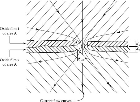
FIGURE 1.47
The a-spot surrounded by oxide films.
(1.32) |
where ρ1, ρ2 and d1, d2 are respectively the resistivities and mean oxide film thicknesses in the electrical interface, and A is the total area of contact. The relative magnitudes of the constriction resistance of the a-spot and Rf may now be estimated for copper-to-copper and aluminum-to-aluminum contacts. Consider an electrical contact in which the area of nominal contact is given as A and has a value of 1 cm2. If the radius of the metal-to-metal a-spot is 10 μm, the area of metal-to-metal contact represents only about 0.0003% of the total contact area, which would represent a highly unfavorable situation in practice. The values of the constriction resistance and Rf calculated respectively from Equation 1.3, using ρ = (ρ1 + ρ2)/2, and Equations 1.29 through 1.32 are listed in Table 1.8. In these calculations, the film thicknesses were taken as 2 nm and the junction temperature assumed to be 100°C. It is clear from the data in Table 1.8 that the resistance presented by the metallic bridge is considerably smaller than that of the surface films, although the contact area provided by the bridge is a small fraction of the total area of contact. In practical electrical contacts, the area of metal-to-metal contact is much larger than 0.0003%, so that current flow through the oxide film can be ignored in comparison to current flow through the metal-to-metal contacts. From Table 1.8, it is clear that contact resistance can be reduced drastically if surface oxide layers are removed or dispersed from the electrical interface.
TABLE 1.8
Values of Constriction Resistance and Film Resistance for the Case Illustrated in Figure 1.47 (Oxide Film Thickness = 2 nm)
Film Resistance (Ω) |
||||
Type of Metallic Junction |
Resistance of Metal-to-Metal α-Spot (Ω) |
Cu2O |
Al2O3 |
Total Film Resistance (Ω) |
Copper–copper |
1.4 × 10⁻³ |
0.09 |
— |
0.18 |
Aluminum–aluminum |
2.9 × 10⁻³ |
— |
11.6 |
23.2 |
FIGURE 1.48
Example of current–voltage characteristics from aluminum–aluminum contact couples in which the surface oxide films were initially unfractured. (From RS Timsit, Can Elect Assoc Rep 76–19, 1976 [80].)
1.3.6 Fritting of Electrically Insulating Surface Films
In the presence of electrically insulating films on metal surfaces, the formation of metal-to-metal a-spots in a bulk electrical interface requires that the films be mechanically disrupted first, as shown earlier in Figures 1.36 and 1.37a. In the absence of the action of mechanical forces to fracture the films, disruption may be achieved by electrically induced breakdown if a sufficiently large electric field is applied across the contact interface. This dielectric breakdown, simultaneously yielding a metal-to-metal contact, has been labeled by Holm as fritting [3]. Film breakdown, leading to immediate melting of metallic bridges formed through the ruptured insulating layers, is usually referred to as A-fritting. It occurs when the voltage across the metallic bridges established through the fractured insulating film is larger than the so-called melting voltage. This melting voltage is usually on the order of 1 V and will be addressed in detail in the following section. If the voltage drop across the contact is sufficient to soften metallic a-spots but not to melt them, the film breakdown is labeled as B-fritting [3]. The two types of fritting are generally observed when metal surfaces covered with tarnish films or oxide layers are brought into contact and the potential difference across the interface is slowly increased. When the electric field strength across the insulating layers reaches a magnitude of the order of 108 Vm−1, fritting occurs and is characterized by a sudden rise in the current caused by the abrupt decrease in the contact resistance when metallic a-spots are formed.
Figure 1.48 shows an example of B-fritting in an electrical interface consisting of two hemispherical oxide-covered aluminum surfaces in vacuum under a mechanical load lesser than 1 N [80]. The curve obtained under a load of 0.33 N gives the resistance of the contact as ~ 7.3 × 10⁶ Ω. This curve indicates some initial electrical instability in the oxide films as the potential is increased because there are obvious signs of hysteresis as the voltage is lowered. The progressive degeneration of the oxide films as the contact load is increased is illustrated by the data obtained at 0.43 N. Here, the current surges rapidly to large values as the voltage drop across the contact is increased to approximately 25 mV. This fritting was probably assisted by mechanical weakening of the oxide surface layers under the larger mechanical load. Several other interesting examples of A-fritting and B-fritting are described by Holm in his classic book [3].
1.4 Temperature of an Electrically Heated a-Spot
The definition of constriction resistance as ρ/2a is valid so long as the electric current through the constriction is sufficiently small and the effect on contact resistance due to heat generated is negligible. Under these conditions, the voltage drop across the constriction produced by an electric current I is simply given as ρI/2a. Under conditions where significant Joule-heating is produced within the constriction, the crowding of current lines within the a-spot generates a thermal gradient normal to that constriction. The effect of this gradient complicates the relationship between voltage drop across the contact, electric current, and dimension of the a-spot. This section examines the nature of this relationship.
On passing an electric current, the temperature of an a-spot rises to a near-equilibrium temperature very quickly. Consider, for example, the heating of a circular constriction of radius a located between two semi-infinite conducting bodies of electric resistivity p and thermal conductivity λ. If ρ and λ are independent of temperature, the differential equation describing the temperature rise in the bodies in spherical coordinates is given as
λ{∂2T∂r2+1r∂T∂r+1r2sin2θ∂2T∂θ2}=c∂2T∂t2+ρj2
where j is the current density at the location (r, θ) and c is the heat capacity per unit volume. The solution to this equation can only be obtained numerically. However, it may be shown [137] that the solution is a superposition of factors of the form
Acexp{−cr24λt}{4πλtc}3/2
Hence in the neighborhood of the constriction where r ~ a, the time constant with which the temperature rises is ca2/4 λ. For electrical conductors such as copper and aluminum, λ and c take values of 400 Wm−1 °C−1 (0.96 cal s−1 cm−1 °C−1) and 3.44 × 10⁶ Jm−3 °C−1 (0.82 cal cm−3 °C−1) for copper, and 236 Wm−1 °C−1 (0.56 cal s−1 cm−1 °C−1) and 2.43 × 10⁶ Jm−3 °C−1 (0.58 cal cm−3 °C−1) for aluminum at room temperature. The time constant is, thus, approximately 2.2 × 10⁻⁷ s and 2.6 × 10⁻⁷ s respectively for copper and aluminum for a constriction with a radius of 10 μm, and decreases rapidly with decreasing constriction radius. The time evolution and spatial distribution of temperature in two semi-infinite bodies separated by a circular constriction of radius a was calculated by Holm [3] and is illustrated in Figure 1.49. The small rise time associated with the heating of an a-spot forms the basis on which thermal transients are usually ignored in dealing with stationary or slowly moving contacts. In these applications, only the equilibrium contact temperature is of interest. Thermal transients are taken into account only in applications of rapidly moving contacts such as brush contacts, or in high-frequency,high-power electrical connections. This section focuses on electrical contacts in a thermal steady state.
FIGURE 1.49
Supertemperature, normalized to the steady-state temperature Tm, as a function of the normalized time τ = (λ/ca2)t, where λ is the thermal conductivity, c is the heat capacity per unit volume, and a is the a-spot radius. The parameter μ is the distance of an isothermal surface located within the contact material, measured from the center of the constriction along the constriction cylindrical axis. The bulk temperature is taken as 0°C far from the constriction. (From R Holm, Electric Contacts, Theory and Applications, Berlin: Springer-Verlag, 2000 [30].)
1.4.1 Voltage–Temperature Relation
The conventional treatment of electrically heated contacts in thermal equilibrium assumes that the outer surfaces of the conductors are thermally insulated from the external environment. The heat produced within an a-spot can, thus, be dissipated only by conduction through the bodies in contact. Under these conditions, it turns out that the electric and thermal current flow lines follow the same paths, and hence the electric potential and isothermal surfaces within the conductors coincide [34,138,139]. This unique relationship between electric and thermal current flow led Kohlrausch (see for example [2,3]) to derive the following simple relation between the voltage drop V across the contact and the maximum temperature Tm in the contact interface as
(1.33) |
where λ and ρ are respectively the thermal conductivity and electrical resistivity of the conductors, the subscripts 1 and 2 refer to the two conductors in contact, and T1 and T2 refer to the bulk temperatures of the contacting bodies. Thermoelectric effects are assumed to be small and are neglected. The quantities λ and ρ generally vary with temperature. Since the electric current flow lines are most constricted within the a-spot, the maximum temperature Tm occurs either within the confines of the a-spot or in its immediate vicinity. For a monometallic contact where λ1 = λ2 = λ and ρ1 = ρ2 = ρ, Tm occurs precisely at the a-spot and the relation reduces to
(1.34) |
Over a temperature range where the quantities λ and ρ vary little with temperature, Equation 1.34 yields the well-known form of the voltage-temperature (V–T) relation for monometallic electrical contacts [3]
(1.35) |
The quantity (Tm – T1) in the left-hand side of Equation 1.35 is defined as the contact super-temperature, that is, the deviation of the a-spot temperature from the bulk connector temperature. Equation 1.35 is often used in the contact literature and in designing electrical connectors to evaluate the expected supertemperature of an electrical interface during operation. Generally, connectors are designed so that the supertemperature does not exceed 1°C–3°C under extreme operating conditions. Under conditions where the supertemperature is large, that is, several tens of degrees Celsius, Equation 1.35 loses its validity since this relation was derived on the basis of constant electrical resistivity and thermal conductivity. As mentioned earlier, both ρ and λ generally vary with temperature. Under these conditions, the V–T relation takes on a more complicated form which will be described below.
Before deriving the more rigorous V–T relation for the case of elevated contact temperatures, it is important to note that the right-hand side Equations 1.33 through 1.35 involves materials properties only through λ and ρ, and makes no reference to contact geometry. The V–T relation is, thus, valid for electrical contacts of any shape and dimensions. An examination of the details of the mathematical derivation reveals that the V–T relation holds for any thermally insulated body capable of passing an electric current. This is illustrated in the following simple example.
Consider an electrically conductive metal bar of length 2L and uniform cross-section A, through which an electric current of uniform density j is passed, as shown in Figure 1.50. The temperature at both ends of the bar is held at a temperature T1. If the conductor is thermally insulated from the surroundings, the differential equation governing the temperature distribution T(x) within the solid is
(1.36) |
FIGURE 1.50
Electrically conducting and thermally insulated bar of uniform cross-section heated by an electrical current of density j.
where λ and ρ are the thermal conductivity and electrical resistivity of the bar material respectively, and x is the distance along the bar. If, for simplicity, λ and p are assumed temperature independent, the solution of Equation (1.36) is straightforward and is given as
(1.37) |
The maximum temperature, thus, occurs at the centre x = 0 of the bar. Since the voltage drop across the bar is given as
V=2ρjL
the difference between the maximum temperature in the rod and the temperature at the ends, that is, the supertemperature, is given as
T(0)−T1=V28λρ
which is identical to Equation 1.35. Thus, Equation 1.35, and more generally Equation 1.33, applies to any thermally insulated body heated by an electric current.
Usually, the dependence of the thermal conductivity and electrical resistivity on temperature can be expressed respectively as λ=λ0(1−βT) and ρ=ρ0(1+αT) over a wide temperature range [3,34], where the subscript 0 refers to the value at 0°C and β and α are the temperature coefficients of thermal conductivity and electrical resistivity respectively. Note the thermal conductivity of metals generally decreases with increasing temperature whereas electrical resistivity increases. The origins of this dependence on temperature are reviewed briefly in Appendix A. The values of λ, ρ at 20°C, β and α for many metals and metallic alloys are listed in Chapter 24. Using these forms of the temperature dependence of λ and ρ produces the following V–T relation from Equation 1.34
(1.38) |
Using the data of Tables 24.1 and 24.10, the calculated dependence of Tm on V for aluminum–aluminum, copper–copper and brass–brass contacts is shown in Figure 1.51 forbulk temperatures T1 of 20°C and 100°C. The curves corresponding to aluminum–copper, copper–brass, and aluminum–brass junctions fall approximately midway between curves 1 and 2, 1 and 3, and 2 and 3 respectively. Note in all cases the contact temperature deviates significantly from the bulk temperature only when the voltage drop across the contact exceeds approximately 10 mV. The potential drops in excess of 0.1 V produce contact temperatures that can easily lead to softening or melting of the contact material. Table 1.9 lists the voltage drop calculated on the basis of Equation 1.38 at which softening and melting of common electrical contact materials occur [3]. Despite the deviation from linearity of the dependence of λ and ρ on T at temperatures approaching the melting point of metals, Equation 1.38 was found to predict values of the melting voltage of many metals in good agreement with measured values [3]. The limits of validity of the V–T relation in electrical contacts were investigated experimentally by Timsit [140]. It was shown that the relation is valid as long as the average diameter of the a-spot is larger than the mean free path of free electrons in the contacting bodies. The V–T relation breaks down when this criterion is violated. This effect is treated in greater detail in Section 1.6.
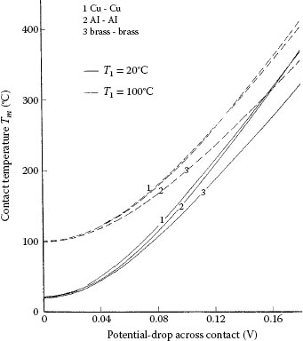
FIGURE 1.51
Voltage-temperature relationship for copper–copper, aluminum–aluminum, and brass–brass electrical contacts for bulk temperatures T1 of 20°C and 100°C.
TABLE 1.9
Voltage for Softening (Vs) and Melting (Vm) of Common Electrical Contact Materials
Material |
Heat Capacity (Jm−3°C−1)×106 |
Vs Softening (V) |
Vm Melting (V) |
Al |
2.4 |
0.1 |
0.3 |
Fe |
3.6 |
0.19 |
0.19 |
Ni |
3.9 |
0.16 |
0.16 |
Cu |
3.4 |
0.12 |
0.43 |
Zn |
0.1 |
0.17 |
|
Mo |
2.6 at 20°C |
0.25 |
0.75 |
3.4 at 1500°C |
|||
Ag |
2.5 |
0.09 |
0.37 |
Cd |
2 |
||
Sn |
1.65 |
0.07 |
0.13 |
Au |
2.5 |
0.08 |
0.43 |
W |
2.7 at 20°C |
0.4 |
1.1 |
3.5 at 1400°C |
|||
3.9 at 2100°C |
|||
Pt |
2.8 |
0.25 |
0.65 |
Pd |
2.7 |
0.57 |
|
Pb |
0.12 |
0.19 |
|
60Cu, 40Zn |
3.2 |
0.2 |
|
60Cu, 40Sn |
3 |
0.15 |
|
Stainless steel |
3.9 |
0.27 |
0.55 |
WC |
3 |
0.6 |
Equation 1.38 is an accurate depiction of the V–T relation, valid over the entire temperature range over which the resistivity and thermal conductivity vary linearly with temperature. For engineering purposes, this relation is difficult to handle. In this section, a simple version of the V–T relation is derived.
Note that all the curves in Figure 1.51 associated with the same bulk conductor temperature lie close together. It may be verified that the V–T curves corresponding to many metals also fall very close to the these curves. This surprising observation stems in part from the Wiedemann–Franz law [3] which states that the variations with temperature of the thermal conductivity and electrical resistivity of metals are such that λ and ρ are related by the expression
(1.39) |
where L is the Lorentz constant (2.45 × 10⁻⁸ V2 K−2) and T is the absolute temperature. Equation 1.39 holds if thermal conduction and electrical resistivity arise from electronic transport in the metals. Although this relation provides a reasonable description of thermal and electrical transport properties in metals over the temperature range generally relevant to ordinary electrical contacts, it is not universally valid. The origin of the Wiedemann–Franz law is discussed in relation to the electrical and thermal conductivity of metals outlined in Appendix A. If the relation in Equation 1.39 holds, then Equation 1.34 immediately yields the rigorously valid V–T relation as
(1.40) |
which is indeed independent of the materials in the contact. Equation 1.40 is not as easy to use as Equation 1.35 because the supertemperature (Tm – T1) cannot be evaluated readily from the voltage drop. It is instructive to compare the values of supertemperature calculated from Equation 1.35 with those evaluated from the more accurate relation in Equation 1.40, for values of V that are generally considered excessive for electrical contacts. Consider a copper–copper contact with a bulk temperature T1 of 20°C. Using the room-temperature values of resistivity and thermal conductivity of copper respectively as 1.75 × 10⁻⁸ Ωm and 380 Wm−1°C−1 in Equation 1.35, the supertemperature evaluated from Equation 1.35 and that yielded by the more accurate relation in Equation 1.40 are shown in Table 1.10 for a number of values of the voltage drop V across the contact. Note the difference is small and insignificant from the engineering viewpoint for voltage drops as large as 0.05 V. This explains the popularity of Equation 1.35 for the evaluation of supertemperature.
Equation 1.40 may be reduced to the form of Equation 1.35 by mathematical redefinition and rearrangement of terms. Defining (Tm+T1)/2 as the average temperature Tavg in the contact, the evaluation of Equation 1.39 at Tavg yields
λavgρavg=L{Tm+T1}2
TABLE 1.10
Comparison of Supertemperatures Evaluated from Equations 1.35 and 1.40
Voltage Drop (V) |
Supertemperature (Tm – T1)/Equation 1.36 (°C) |
Supertemperature (Tm – T1)/Equation 1.41 (°C) |
0.005 |
0.47 |
0.44 |
0.01 |
1.9 |
1.7 |
0.02 |
7.5 |
6.9 |
0.03 |
17 |
15 |
0.04 |
30 |
27 |
0.05 |
47 |
41 |
It follows that {T2m−T12}={Tm−T1}×{Tm+T1}={Tm−T1}2λavgρavg/L. Substituting this expression into Equation 1.40 yields
Tm−T1=V28λavgρavg
and the V–T relation in Equation 1.35 is recovered with the physical parameters λ and ρ evaluated at the average connector temperature. Because Equation 1.40 is independent of the specific electrical and thermal conductivity properties of the materials in the contact, it applies equally well to monometallic and bimetallic contacts provided the Wiedemann–Franz law applies to both contact materials. The validity of the Wiedemann–Franz law does not necessarily imply that the maximum contact temperature occurs at the location of the physical interface.
1.4.4 Temperature Distribution in the Vicinity of an a-Spot
The calculation of the temperature distribution within an a-spot is facilitated by the geometrical coincidence of the equipotential and isothermal surfaces within the volumes of the conductors. This calculation needs information additional to that for Equation 1.34. Following Holm [3], Greenwood and Williamson [34] showed that the maximum contact temperature Tm and the current I are related by the expression
RCI=ρ1,0Tm∫T1{2Tm∫Tλ1ρ1dT′}−1/2λ1dT+ρ2,0Tm∫T2{2Tm∫Tλ2ρ2dT′}−1/2λ2dT |
(1.41) |
where T1 and T2 are the bulk temperatures respectively of materials 1 and 2, RC is the “cold” contact resistance, ρ10 and ρ20 are the “cold” resistivities respectively of materials 1 and 2 defined through the dependence on temperature of the electrical resistivity, that is, ρ=ρ0(1+αT), and λ1 and λ2 are the thermal conductivities respectively of materials 1 and 2. Equation 1.41 is remarkable as it shows the maximum temperature developed in a contact is related to the voltage drop developed by the same current, if the identical contact had remained cold, since RCI is the “cold” voltage drop. Using again the temperature dependence λ=λ0(1−βT) and if β is sufficiently smaller than α (e.g. β∼α/20 for copper),the integral in Equation 1.41 is given approximately as
Tm∫T1{2Tm∫TλρdT}−1/2λdT′=(λ0{α−β}ρ0)1/2{αα−β}cos−1(1+{α−β}T11+{α−β}Tm) |
(1.42) |
For a monometallic junction and bulk temperatures T1 and T2 of 0°C, RC is given as ρ0/2a, so Equation 1.41 becomes
(1.43) |
Similarly, at an equipotential surface at a temperature T and located at a finite axial distance μ from the constriction, RC is given as (ρ0/πa)tan−1(μ/a) from Equation 1.1. Equation 1.41 then becomes [34]
(1.44) |
Equating Equations 1.43 and 1.44 yields the dependence of the temperature T at the isothermal surface located at a distance μ from the constriction
(1.45) |
The variations of temperature both in the plane of and normal to the constriction, are illustrated in Figure 1.52 for the special case of β=0°C−1,α=4×10⁻³°C−1 and Tm=1000°C [34]. Note the temperature decreases to that of the bulk over a distance of only several constriction diameters.
1.4.5 Deviation of the Voltage–Temperature Relation in an Assymetric Contact
1.4.5.1 Case I: Two Metals in Contact
In a bimetallic contact, the maximum temperature developed within an a-spot would be expected to occur within the material with the larger electrical resistivity, rather than at the interface between the two metals. However, simple arguments given in Appendix B show that the deviation of the interfacing temperature from the maximum temperature is not expected to be large and the maximum temperature generally occurs in the immediate vicinity of the physical interface even when the resistivities of the contacting materials differ significantly. For all practical purposes, the maximum temperature may, thus, be considered to occur at the physical interface between the two materials. This situation is descriptive of bimetallic contacts involving good electrical conductors such as aluminum, copper, brasses, copper bronzes and so on, but is generally not applicable to interfaces in which highly dissimilar materials, such as copper and graphite, are used.
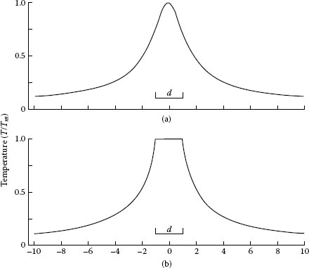
FIGURE 1.52
Steady state temperature distribution within a conductor under conditions where the thermal conductivity is constant and the resistivity varies with temperature as ρ0(1+αT), where α=4×10⁻³°C−1,Tm=1,000°C, and d is the constriction diameter 2a [34] (a) Temperature along the cylindrical axis of the constriction (b) Temperature in the plane of the interface. (From JA Greenwood and JBP Williamson, Proc Roy Soc A246: 13, 1958 [34].)
(a) Distance from constriction plane, z/a
(b) Radial distance from center of constriction, r/a, in constriction plane
1.4.5.2 Case II: A Metal in Contact with a Non-Metal
In electrical contacts where the electrical conductivities of the contacting materials are vastly different, such as in copper–graphite contacts, the surface corresponding to the maximum temperature is much more deeply embedded in the material with higher resistivity than the calculation in Appendix B indicates for Case I. The location of the surface at which the maximum temperature is produced depends on the geometry of the contact. An illustrative example of this effect for the case of a copper–graphite contact is described in detail in Appendix C.
1.4.6 Special Considerations on the “Melting” Voltage in Electrical Contacts
We recall that the voltage–temperature relation was derived on the assumption of equilibrium between ohmic heating in the electrical constriction and thermal dissipation by conduction within the contacting materials. This relation was used to evaluate the potential drop required across a contact to cause melting of the electrical interface. The calculated melting voltage for several metals is listed in Table 1.9.
FIGURE 1.53
Generic dependence on temperature of electrical resistivity and thermal conductivity of metals.
As mentioned earlier, the electrical resistivity of metals increases whereas thermal conductivity generally decreases with increasing temperature, as illustrated schematically in Figure 1.53. In metal contacts, an increase in electric current generally leads to a rapid increase in temperature of the a-spot due to a combination of events: the increased thermal dissipation generated by the larger current causes an increase in temperature which in turn, increases resistivity and hence further increases ohmic heating; the increased temperature also decreases thermal conductivity which reduces the ability of the junction to dissipate heat by thermal conduction. With good electrical conductors such as aluminum and copper conductor alloys, the rise in electrical resistivity and the decrease in thermal conductivity with increasing temperature are sufficiently slow so the a-spot reaches the equilibrium temperature defined by Equation 1.40. In other metals such as Ni and Fe, the increase in resistivity and decrease in thermal conductivity associated with increasing temperature is relatively rapid. In electrical contacts made from these metals, a critical voltage is found to exist at which heat can no longer be dissipated at a rate compatible with the requirements for thermal equilibrium. At this critical voltage, a small rise in temperature increases the resistivity and decreases the thermal conductivity in the a-spot sufficiently to cause significant additional heat entrapment. This, in turn, rapidly boosts the contact temperature, which leads to a further large drop in thermal conductivity, and so on. Thermal equilibrium is, thus, never attained. This condition leads to effective entrapment of ohmic heat with ensuing thermal runaway and contact melting. The critical voltage for the onset of this phenomenon is generally appreciably smaller than the conventional melting voltage [34,141].
It was stated in Equation 1.33 that the potential drop V across a thermally insulated junction is related to the electrical and thermal properties of the contact materials as
V={2Tm∫T1λ1ρ1dT}1/2+{2Tm∫T2λ2ρ2dT}1/2
Similarly, it was indicated in Equation 1.41 that the total current I through the contact is related to λ, ρ and the dimensions of the contact spot as
(1.46) |
where
F(λ,ρ,Ti,Tm)=ρ0Tm∫Ti{2Tm∫TλρdT}−1/2λdT
and RC is the “cold resistance” of the contact, which depends on the contact geometry. The numerical evaluation of the function F(λ,ρ,Ti,Tm) is straightforward if the dependence of λ and ρ on temperature is known. This dependence can be expressed as a power series of temperature and may include more powers of T than used in the evaluations of Equations 1.38 and 1.42. This more detailed dependence may be expressed as
ρ=ρ0{1+αT+γT2+ηT3} and λ=λ0{1−βT+δT2+εT3}
so that
λρ=λ0ρ0(1+{α−β}T+{δ+γ−αβ}T3)
over a wide temperature range. Table 1.11 lists the values of the required constants for a number of electrical contact materials [141].
For a monometallic contact, Equation 1.46 reduces to
IRC=2F(λ1,ρ1,T1,Tm)
or
(1.47) |
Note the dependence on temperature of the right-hand side of Equation 1.47 arises solely from the parameters of the materials. Figure 1.54 shows the variation with Tm of the quantity 2F(λ1,ρ1,T1,Tm)/ρ0 for the electrical couples listed in Table 1.11. The evaluations were carried out for a value of T1 of zero, that is, where the temperature of the contacts far removed from the junction is 0°C. For the nickel–aluminum system, the curve plotted in Figure 1.54 corresponds to the quantity 2(F[λ1,ρ1,T1,Tm]+F[λ2,ρ2,T2,Tm])/(ρ1,0+ρ2,0), where the subscripts 1 and 2 refer respectively to aluminum and nickel.
For Al, the function F=F(λ,ρ,0,Tm) increases up to the melting point of the metal. For Fe, Ni, and W, the function reaches a maximum at T*m and then decreases. The maximum is broad and its location is sensitive to the materials parameters, λ and ρ. The existence of this maximum defines a thermal instability leading to the thermal runaway effect outlined above. The nature of this instability may be understood as follows.
In the case of aluminum–aluminum contacts Equation 1.47 is always satisfied since an increase in the value of I, leading to a larger value of the left-hand side of the equation, can always be matched by an increase in the right-hand side through a larger value of Tm. Thus, an increase in electric current always leads to a higher contact temperature, up to the melting point of aluminum—660°C. In the case of iron and nickel, there is a critical temperature corresponding to the maximum of the function F at which any increase in the magnitude of I can no longer be matched by the function F, that is, Equation 1.47 breaks down. Physically, a condition is reached where ∂Tm/∂I→∞, and thus where the slightest increase in current generates a disproportionally large increase in temperature leading to contact melting. The calculated values of the critical temperature T*m for the systems of interest are listed in Table 1.11. This temperature is much lower than the melting point of the respective metals. The calculated melting voltages for iron–iron and nickel–nickel contacts are respectively 0.19 V and 0.16 V [141]. Figures 1.55a and 1.55b show the drop in potential across Fe/Fe and Ni/Ni contacts, and the corresponding bulk temperature T1 in the contacting bodies, as the current is increased [141]. Note the onset of melting (“premature” melting) at 192 mV in iron and at 164 mV in nickel. These values are in excellent agreement with the calculated values [141].
TABLE 1.11
Electrical Resistivity and Thermal Conductivity Constants
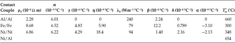
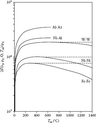
FIGURE 1.54
Dependence of the function 2F(λ,ρ,0,Tm)/ρ0 on the contact temperature Tm. (From RS Timsit, IEEE Trans Comp Hyb Manuf Tech CHMT-14: 285, 1991 [141].)
Finally, note that the “melting” temperature of nickel–aluminum contacts is nearly identical with the melting point of aluminum. The effect of replacing one side of a nickel–nickel contact with a surface of large thermal conductivity, thus enhancing thermal dissipation, has a considerable effect on the “melting” temperature. “Premature” melting of electrical contacts, as described above, does not occur in common electrical contact metals such as copper, copper-based brasses and copper-based and aluminum-based bronzes.
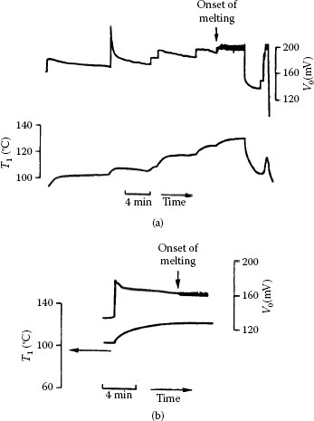
FIGURE 1.55
(a) Onset of melting in an iron–iron electrical interface; each discontinuity in the potential drop V0 across the contact (top) is due to a steep increase in the current (b) Onset of melting in a nickel–nickel electrical interface; the sharp increase in the potential drop across the contact (top) arises from a steep increase in the current. In (a) and (b), the bottom curve represents the bulk temperature T1. (From RS Timsit, IEEE Trans Comp Hyb Manuf Tech CHMT-14: 285, 1991 [141].)