
1.5 Mechanics of a-Spot Formation
In an electrical interface, metal-to-metal a-spots are subjected to a variety of mechanical forces that influence the shape and dimensions of spots with time, even in apparently stationary junctions. It is well known that clean smooth surfaces pressed into intimate contact may adhere strongly under the action of intermolecular forces [15,142]. Figure 1.37b illustrated the dependence of contact resistance on mechanical load obtained with smooth oxide-free aluminum surfaces generated in ultra-high vacuum [80]. As the load was increased, the resistance dropped rapidly to a low value and remained relatively constant during the unload phase. As is evident in the figure, the oxide-free surfaces were firmly bonded together after contact was established and required the application of a relatively large tensile load to bring about separation. Figure 1.56 shows the dependence of the load required on the contact area to separate smooth and clean hemispherical AA1350 aluminum surfaces pressed into contact in ultra-high vacuum at room temperature. The aluminum had been annealed at 300°C. The radius of curvature Rsur of the surfaces was 0.254 m [80]. The contact area was varied by varying the mechanical load applied to the interface. The radius of the metal-to-metal contact area was calculated from Equation 1.4
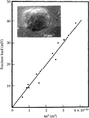
FIGURE 1.56
Load required to separate clean, oxide-free aluminum surfaces in ultra-high vacuum, as a function of the area πa2 of metal-to-metal contact. Inset: micrograph of a contact spot after a measurement of fracture strength after applying a contact load of a few mN (see Figure 1.37); the circle was drawn on the basis of the radius a calculated from the contact resistance measured before fracture. (From RS Timsit, Can Elect Assoc Rep 76–19, 1976 [80].)
RC=ρ2a(1−1.416{aR}+…..)
after measuring the contact resistance at room temperature [80]. The slope of the average straight line in Figure 1.56 yields a fracture stress at the interface of 99 MPa. This is identical with the fracture stress of H12 AA1350 aluminum, suggesting cold-working of the aluminum in the a-spot. The inset of Figure 1.57 shows the micrograph of an actual contact spot after measuring the fracture strength of the hemispherical interface. The radius of the circle represents the radius calculated from a measurement of contact resistance. The agreement with the actual periphery of the contact confirms the validity of the evaluation procedure for determining the contact radius.
If two elastic surfaces of radius of curvatures, R1 and R2 are pressed into contact by a force T, according to Hertz [143] the surfaces make contact on a circle of radius a given by the expression
(1.48) |

FIGURE 1.57
Typical dependence of contact resistance on time in ultra-high vacuum (pressure ~ 10−10 torr) immediately after rupture of interfacial oxide films. (From RS Timsit, IEEE Trans Comp Hyb Manuf Tech 3: 71, 1980 [99].)
with R′=R1R2R1+R2, K=4E3 and 1E={1−v21}E1+{1−v22}E2
where E1 and E2 are Young’s modulus and ν1 and ν2 are Poisson’s ratio for the materials of surfaces 1 and 2 respectively. In the presence of adhesive forces between the surfaces, it was shown by Johnson et al. [144] that Equation 1.48 becomes
a={R′K[P+3πγsR′+(6πγsR′P+{3πγsR′}2)1/2]}1/3
where γs is the surface energy at the contact interface. It follows that an equilibrium contact area can be maintained even in the presence of a tensile force, up to a maximum value of
(1.49) |
which is the force required to separate the spheres, whereR′=Rsur/2. Compare now the prediction of Equation 1.49 with the data of Figure 1.56. For aluminum surfaces, the surface energy is of the order of 1 Jm−2 [145]. For hemispherical surfaces with Rsur = 0.254 m, the maximum tensile force given by Equation 1.49 is thus 1.2 N and is independent of the applied load. The fracture loads shown in Figure 1.56 were all considerably smaller than this value and were found to vary with applied load, since the contact radius was increased by applying larger loads. The increase in contact radius with increased load stems from plastic deformation in the contact, that is, as indicated by Equation 1.10. The observation that the fracture load was always considerably smaller than 1.2 N is due to the presence of structural defects in aluminum. This is known to lower the strength to far below the theoretical limit [146].
The data of Figure 1.56 were obtained from contact a-spots with a radius ranging from a few to several microns. In the presence of electrically insulative surface oxide films, the a-spots in aluminum contacts are formed through fissures in these films. If the films are not mechanically dispersed, a-spots may only be formed by extrusion of metal across the electrical interface and are generally smaller than indicated in Figure 1.56. Because the formation of metal bridges is a dynamic process, it would be expected that the area of metal-to-metal contact would increase for some time interval following generation of the a-spot. Figure 1.57 shows the typical variation with time of the contact resistance of an electrical interface formed by two smooth AA1350 aluminum surfaces pressed into contact at room temperature in ultra-high vacuum [99]. The surfaces were chemically clean but were covered with an aluminum oxide layer approximately 3 nm thick by exposure to oxygen, and a constant mechanical load was maintained. The contact resistance was found to decrease with time whenever the area of metallic contact was sufficiently small, that is, the area of electrical contact was found to grow under constant mechanical load. Figure 1.58 shows typical variations with time of the average radius of electrical contact in these interfaces, where a0 is the initial electric contact radius at time t = 0. The striking feature of the data of Figure 1.58 is the eventual tendency of the curves to a straight line with slope dln(a/a0)/dln(t) of approximately 1/9 [99,147]. A detailed examination of these curves reveals that mechanical load has no apparent effect on contact growth over the range of loads used in the investigation.
The data of Figure 1.58 can be interpreted in terms of a sintering mechanism. Figure 1.59 illustrates a contact spot formed through cracks in oxide films in an aluminum–aluminum interface. For simplicity, the spot is assumed circular with a radius a. The surfaces in the immediate vicinity of the neck are assumed locally distorted approximately as spheres with an average radius of curvature rs. Sintering describes a bonding mechanism between surfaces in which the contact area (and hence, the neck of the contact) grows as a result of transport of material from the immediate vicinity of the contact interface into the contact region as a result of some driving force. By far the most important driving force for mass transport in conventional sintering is that due to surface tension [148]. If S is the surface area of the contact neck of Figure 1.59, then the surface energy U is simply given as γsS, where γs is the surface energy of the solid. Since the system is in thermodynamic equilibrium only under conditions where U is a minimum, the neck grows until the surface S is minimized. The effective force F acting axially outward to induce the growth is, then, given as

FIGURE 1.58
Typical growth of contact radius a in vacuum at low loads; the value of the initial contact radius a0(in nanometers) and the contact load corresponding to each curve are respectively: ● 4 N and 0.19 N; ○ 100 N and 0.19 N; □ 73 N and 0.20 N; 100 N and 0.20 N; × 12 N and 0.20 N; ▴ 84 and 0.30 N; △ 96 and 0.37 N. (From RS Timsit, IEEE Trans Comp Hyb Manuf Tech 3: 71, 1980 [99]; RS Timsit, Appl Phys Lett 35: 400, 1979 [147].)
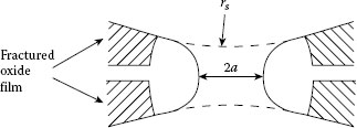
FIGURE 1.59
Schematic diagram of contact spot formed between cracks in aluminum oxide surface films.
F=−dUdr
Early et al. [149] have shown that this force gives rise to a mean radial stress, σ on the neck surface given as
(1.50) |
when a is much smaller than the mean local radius of curvature rs of the surfaces. Taking ys for aluminum as 1 Jm−2 [145] and a as 10−7m yields σ ~ 30 MPa; the radial stresses induced on the contact neck by the surface tension can, thus, be large when the junction is narrow.
When the stresses induced by the surface tension are sufficiently large, the contact junction will generally grow. The transport of material required to feed the growth can occur through one or a combination of several well-established mechanisms [150] such as surface diffusion, volume diffusion, grain–boundary diffusion and creep [151]. At room temperature, sintering fed by dislocation creep represents a mechanism that can explain much of the data of Figure 1.58 [99,147]. It has been demonstrated that interfaces such as grain boundaries and free surfaces are the most common sources of dislocations [152]. A threshold stress is required to generate dislocations from such sources. In the contact situation under consideration, this threshold stress can easily be provided by the surface tension force described above.
In aluminum, at a homologous temperature above approximately 0.3 [153], that is, at temperatures above 10°C, and at relatively large stresses, the strain rate ε̇ induced by dislocation creep is found experimentally to obey the constitutive law [154]
(1.51) |
where n is nearly equal to 4.5 and where κ0 is a constant dependent on temperature. At 300K κ0 = 1.2 × 10−48s−1 Pa−9/2. From the work of Kuczynski et al. [155], it can be shown that if sintering between two spheres is controlled by the creep law given by Equation 1.51, the neck radius increases with time according to
(1.52) |
where rs is the radius of the sintering spheres. In Equation 1.52, length and time units are meters and seconds respectively. Equation 1.52 indicates that after a sufficiently long time when a > a0,
ln{aa0}~19lnt+C
where C is a constant. Thus, the growth curves approach a straight line with a slope of 1/9 on a log–log plot. Within the scatter of the experimental data, this is, indeed, the behavior of the a-spot data in Figure 1.58.
The effect of oxygen on the growth of a-spot in Figure 1.58 is illustrated in Figure 1.60. The properties of the contacts appeared identical at oxygen pressures of 50 torr and 100 torr. A comparison of the curves of Figures 1.58 and 1.60 indicates that contact growth is considerably hampered by the presence of oxygen: the growth rates are smaller than those obtained in vacuum and the curves generally reach a plateau in a reasonably short time. The curves bear no apparent relation to normal load. The contact growth in the presence of oxygen can be qualitatively understood in terms of the sintering model in that, in the presence of oxygen, the contact neck is covered with a surface layer of aluminum oxide with a thickness of several nanometers. The effect of the oxide film on creep is both to alter the image stresses on dislocation mobility [156] and to “strengthen” the contact neck [157], that is, the neck is effectively made from a composite material. These two factors would combine to reduce creep and could account for the relatively slow sintering rate observed with oxygen.
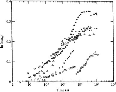
FIGURE 1.60
Typical increase in contact radius a with time in the presence of oxygen gas at a contact load of approximately 0.5 N. The value of a0 (in nanometers) corresponding to each curve is given below. At 50: □ 49; △ 8; ● 49; ▲ 20; at 100 torr: × 5. (From RS Timsit, IEEE Trans Comp Hyb Manuf Tech 3: 71, 1980 [99]; RS Timsit. Appl Phys Lett 35: 400, 1979 [147].)

FIGURE 1.61
Typical dependence on time in oxygen gas (160 torr) of the average a-spot radius (●) and the contact temperature Tm (O); the radius a0 at t = 0 is 2.9 μm. (From RS Timsit, Appl Phys Lett 35: 400, 1979 [147].)
At elevated temperatures, the sintering rate increases rapidly with increasing contact temperature even with oxygen, and contact growth no longer requires a small a-spot. Figure 1.61 illustrates the growth of an a-spot in an aluminum–aluminum contact formed between two hemispheres operated in oxygen at a pressure of 160 torr and carrying a constant DC current of 13.6 A. The initial contact spot radius was determined as 2.9 μm and the initial contact temperature was approximately 232°C (405 K) [158]. Note the relatively rapid increase in a-spot radius. The radius increased to ~ 14.5 μm after approximately 14 hours, leading to a decrease in contact temperature of about 30°C. In this instance, the growth of a-spots in aluminum–aluminum contacts operated at elevated temperatures could be explained in terms of sintering driven by volume diffusion [158].
It is likely that sintering explains at least some of the contact phenomena related to the growth of a-spot observed in gold contacts [20]. Sintering is also probably responsible partially for “self-healing” of electrical contacts as observed by several workers [159,160]. On the other hand, it is unlikely that sintering plays a major role in contacts in which large-scale cold welding occurs [161], as has been reported in highly-crimped junctions at room temperature [162]. In these situations, cold-welded spots are so large that the mechanical stress on a-spot surfaces as given by Equation 1.50 would be too small to induce mass flow.
It was mentioned in Section 1.2.3 that surface asperities undergo plastic deformation in most practical electrical contacts. This led to the conclusion that the true area of mechanical contact depends only on contact force, and is independent of the nominal contact area. It turns out that this relationship between contact force and contact area is more general and holds even when asperity deformation is not purely plastic. Several models of rough surfaces in contact have been proposed in which model asperities are assumed to have elastic or plastic deformation [2,163,164,165] or are treated in terms the random nature of the surface profile [166,167]. If it is assumed that the asperities have the same radius of curvature and deform elastically and independently according to Hertz theory [143], Greenwood and Williamson [2] showed that the area AC of true contact increases rapidly with increasing contact load and is independent of the nominal contact area. This is illustrated in Figure 1.62 where AC curves were calculated for nominal contact areas of 1 cm2 and 10 cm2 using the following parameter values: density of surface asperity of 300 mm−2, the average asperity radius of curvature βav and the rms (root mean square) roughness σsd are such that βavσsd=10−4mm2 and E′(σsd/βav)1/2=245 MPa, where E′ is E/(1−v2) [2]. The curves show that for a given nominal area, the area of true contact is almost exactly proportional to the load. In addition, the two curves for nominal contact areas of 1 cm2 and 10 cm2 are almost indistinguishable, showing that the contact area depends on the load and not on the nominal pressure. Similarly to the explanation provided in Section 1.2.3 with respect to asperities with plastic deformation, the near independence of true contact area on nominal pressure in Figure 1.62 stems from the proportional increase in the number of contacting asperities with nominal contact area at a given load, thus decreasing the pressure on each asperity. This, in turn, decreases the true contact area at each asperity and almost exactly offsets the area gain due to the larger nominal contact.
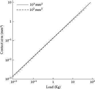
FIGURE 1.62
Relation between area of contact and mechanical load in an interface characterized by material parameters described in the text. The contacting surface asperities are assumed to deform elastically only. The solid curve, for a nominal area of 10 cm2, and the broken curve, for a nominal area of 1 cm2, show that the real area of contact is essentially independent of the nominal area. (From JA Greenwood and JBP Williamson, Proc Roy Soc A295: 300, 1966 [2].)
In order to determine the extent of plastic deformation of contacting asperities, Greenwood and Williamson [2] defined a plasticity index ψ as
ψ = E′H√σ*sdβav
where E′ is E/(1−v2), σ*sd is the standard deviation of the asperity height distribution and βav is the average asperity radius. According to the definition, plastic flow will be significant if ψ > 1, otherwise the asperities deform essentially elastically. From Table 24.1, it may be verified that the ratio E′/H is on the order of 200–400 for most electrical contact materials of interest. Since the ratio σ*sd/βav is seldom smaller than about 5 × 10⁻³ for rough surfaces [2], it is clear that ψ is generally > 1 and contact asperities deform in plastic manner in electrical interfaces of practical connectors. This, again, validates the almost universal use of Equation 1.10 in relating true contact area to contact load in electrical interfaces. It is worth pointing out that contact asperities may not deform in plastic manner in devices such as Micro-Electrico-Mechanical Systems (MEMS) where the contact surfaces are very smooth and where σ*sd/βav may be very small (see Chapter 10).
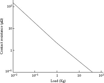
FIGURE 1.63
Dependence of electrical contact resistance on load corresponding to the data or Figure 1.62; the assumption is made that all the contact spots are electrically conducting. (From JA Greenwood and JBP Williamson, Proc Roy Soc A295: 300, 1966 [2].)
The decrease in electrical contact resistance associated with the curves of Figure 1.62 is shown in Figure 1.63[2]. The data of Figure 1.63 was calculated using a resistivity of 2.4 × 10⁻⁸ Ωm and on the assumption that all contacting asperities deform elastically and all contacting area are electrically conducting. The result approximates to the simple law that resistance is proportional to (load)−0.9. In practical electrical contacts, where asperities show plastic deformation, note the area of true contact increases less rapidly than suggested in Figure 1.63 and contact resistance varies as (load)−0.5 (see Equation 1.11).
Plastic deformation of asperities does not necessarily mean that surface asperities flatten out completely under the action of a sufficiently large mechanical compressive load. Moore [168] was the first to demonstrate the remarkable persistence of surface asperities under conditions of bulk plastic flow of a surface. In further investigations of this phenomenon, Williamson and Hunt [169] and Pullen and Williamson [170] confirmed the persistence of the asperity, as illustrated in Figure 1.64 [169], and showed the nominal and real areas of contact are proportional in local indentations. These workers also showed the real area of contact in a locally plastic indentation is affected by the hardness of surface layers relative to that of the bulk deformed material. These effects are illustrated for the case of aluminum in Figure 1.65. In these plots, the filled and unfilled data points represent respectively the nominal area of flat coupons of different dimensions and the real area of contact measured with each coupon. In specimens that were initially annealed and then bead-blasted, that is, where the hardness of the surface layers was larger than the bulk hardness of the material, the ratio of the true area to nominal area of contact was approximately 37%. In specimens that had been work-hardened and then bead-blasted, that is, where the surface roughness was approximately identical to the previous specimens but where the hardness of the surface was identical to that of the bulk metal, the contact ratio was about 50%. Similar results were obtained on gold [169]. These results were explained in terms of the movement of valley floors towards the contact interface as asperities are flattened under the compressive load [169,170]. The implications of these findings as regards electrical contact resistance are clear: the hardness of a contact surface must not be larger than that of the bulk material if the true area of contact is to be maximized.
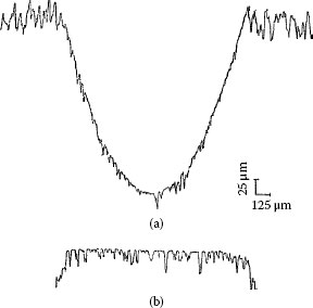
FIGURE 1.64
Two profiles of the same indentation made in aluminum by a smooth steel ball: (a) Normal profile showing the microscopic spherical indentation (b) Same profile as (a) but compensated to remove the macroscopic curvature, showing that persistence in asperity is uniform over the depression. (From JBP Williamson and RT Hunt, Proc Roy Soc A327: 147, 1972 [169].)
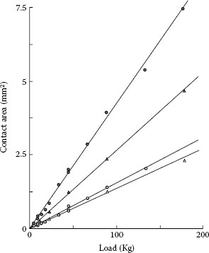
FIGURE 1.65
Dependence of true area of contact on applied load for a spherical indentation in aluminum. ● and ○ show respectively the nominal area of test coupons and true area of contact measured from the coupons: Annealed then bead-blasted specimen; the ratio of true contact area to nominal area is approximately 37%. ▲ and △ show respectively the nominal and true area of contact: Work-hardened and then bead-blasted specimen. The ratio of true area to nominal area is approximately 50%. (From JBP Williamson and RT Hunt, Proc Roy Soc A327: 147, 1972 [169].)
In later years, efforts were made to generate micromechanical models to predict the evolution of microtopography of the surface in a frictional interface. Although these models have focused on metal-working interfaces, the results obviously apply to electrical contacts. For example, Wilson and Sheu [171] modeled asperity deformation produced by flattening against a smooth rigid tool surface. Upper-bound analysis was used to evaluate the resistance to flattening of the asperities as a function of the underlying bulk strain rate, and simple kinematics then related the change in real contact area between the surfaces with increasing bulk deformation. The model took account of the motion of valley floors towards the contact interface during deformation. The validity of the results of this analysis appears to be confirmed by experimental data obtained using wedge-type asperities generated on aluminum strip [171].
In more recent years, a number of different methods to model the contact of rough surfaces have been proposed, including fractal [172], and multiscale models [173,174,175,176,177]. The methods based on fractal mathematics were derived to account for different scales of surface features not accounted for by the statistical models. The multiscale models were developed to alleviate the assumption of self-affinity imposed by fractal mathematics and also to improve the understanding of the conditions of mechanics. Other analyses [176] have used a Fourier transform to convert two-dimensional surface roughness profiles into a series of stacked sinusoids. These methods yielded results that agree with the prediction trends of the earlier work, and differences from the earlier results were often only small [178].
The flattening of a rough surface under pressures greater than the material yield stress has been studied extensively by Wanheim [179] and Bay and Wanheim [180,181,182]. By flattening aluminum specimens with triangular wedge-type asperities in a coining die, these workers were able to verify a slip line field model for flattening of the asperity. Interaction of deformation zones in neighboring asperities caused the rate of flattening to decrease with increasing pressure. Makinouchi et al. [183] performed experiments in which aluminum specimens with wedge-type asperities were flattened in a rig that allowed plain strain compression of the specimen bulk. Their results indicate that no appreciable increase in flattening resistance occurs up to the maximum contact area ratio of 90%. These results are consistent with the predictions of their finite element model, which also allows for bulk plastic strain and bulk flow.
1.6 Breakdown of Classical Electrical Contact Theory in Small Contact Spots
1.6.1 Electrical Conduction in Small a-Spots
We recall that the classical expression for contact resistance as given by Equation 1.3 is based on a solution of the equations of classical electromagnetism where electrical flow is assumed continuous as illustrated in Figure 1.66a. On a sufficiently small scale in solids, electric current flow is not continuous, but occurs through the irregular motion of electrons as they collide with lattice imperfections, defects, and other obstacles in a conductor or an interface. As the constriction in an electrical contact interface approaches the scale at which electronic scattering events occur, the simple concept of classical electrical flow through the constriction becomes increasingly less valid. Thus, as the constriction gets smaller, the electronic flow across may be viewed increasingly as “particulate” as illustrated schematically in Figure 1.66b.
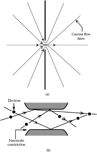
FIGURE 1.66
(a) Classical electric flow through a constriction (b) Ballistic motion of electrons through a small constriction.
As pointed out in earlier publications [184,185], the electrical resistance of a sufficiently small contact spot acquires a so-called Knudsen resistance component in addition to the ohmic component described by Equation 1.3. This additional component arises from the scattering of conduction electrons by the constriction boundary, and becomes prominent in junctions where the constriction radius is smaller than the mean free path lfp of the electron in the conduction medium. The problem of electronic conduction through a circular constriction of radius smaller than lfp resembles the well-known Knudsen problem in kinetic gas theory wherein gas molecules effuse through a small aperture. If the aperture diameter becomes comparable with the mean free path for molecular collision within the gas, the molecules no longer diffuse across the aperture but pass through the orifice ballistically. In the electrical analog, the different electronic conduction regimes are characterized by the Knudsen ratio, K=lfp/a where a is the constriction radius.
Consider first an electrical constriction in the limit of a large Knudsen ratio where conduction is highly ballistic. The electrons are injected into the constriction, and hence pass through the contact ballistically, as illustrated in Figure 1.66b. Sharvin [184,186,187] realized the peculiar electronic transport through a contact in the ballistic regime and calculated the resistance of a constriction of radius a as
(1.53) |
where ρ is the resistivity of the material. Since ρ can be written as [Appendix 1,154]
ρ=mvFne2lfp
where n is the free electron density in the metal, m is the electronic mass and vF is the Fermi velocity, Equation 1.53 reduces to
(1.54) |
where C is a constant dependent only on the electronic properties of the conductor. Since the quantities vF and n are relatively insensitive to temperature over the temperature range of interest here [188], C is also essentially independent of temperature. The Sharvin constriction resistance given in Equation 1.54 is thus largely independent of temperature.
Between the classical and ballistic electronic conduction regimes, the constriction resistance has been shown by Wexler [185] to be given as
(1.55) |
where Γ{K} is a function decreasing from 1 to 0.694 as lfp/a increases from 0 to ∞, as shown in Figure 1.67. It may be verified that Equation 1.55 can be written
(1.56) |
where C is defined in Equation 1.54. Thus, the second term in the right-hand side of Wexler’s expression is the Sharvin resistance. Table 1.12 lists the resistivity and electronic mean free lfp at room temperature of a few commonly-used unalloyed electrical contact materials of high purity [189]. Using known values of m, vF and n,, for a number of contact materials [187,188,189,190], Table 1.12 also lists the value of C in Equation 1.56 to allow an evaluation of contact resistance in the presence of the Sharvin resistance for the respective metals [191]. Figure 1.68 shows the variation of constriction resistance of a copper–copper contact consisting of a single a-spot at room temperature, as a function of the radius a [191]. The two curves correspond respectively to the classical constriction resistance evaluated from Equation 1.3 and the resistance evaluated from Equation 1.56, using the values of ρ and C listed in Table 1.12. Note, the effect of the Sharvin resistance, giving rise to a larger constriction resistance, begins to be significant for a constriction radius smaller than about 100 nm. Similar results are obtained for the other metals listed in Table 1.12.
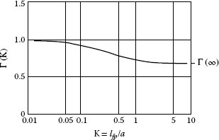
FIGURE 1.67
Dependence of Γ{K} on K. (From G Wexler, Proc Phys Soc 89: 927, 1966 [185].)
TABLE 1.12
Electrical Resistivity and Electronic Mean Free Path at Room Temperature
Metal |
Electrical Resistivity (Ωm) |
Electronic Mean Free Path lfp (nm) |
C × 1016 (Ωm2) |
Al |
2.74 × 10⁻⁸ |
14.5 |
1.70 |
Cu |
1.70 × 10⁻⁸ |
38.7 |
2.79 |
Ag |
1.61 × 10⁻⁸ |
52.3 |
3.57 |
In |
8.75 × 10⁻⁸ |
6.1 |
2.27 |
Sn |
11.0 × 10⁻⁸ |
4.1 |
1.91 |
Au |
2.20 × 10⁻⁸ |
38.3 |
3.58 |
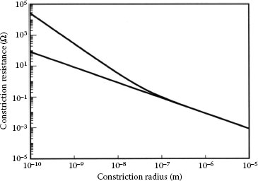
FIGURE 1.68
Constriction resistance for a copper-copper contact at room temperature, as a function of the constriction radius a as calculated from classical contact theory (Equation 1.3) and from Equation 1.57, using the parameter values appropriate to copper in Table 1.12. (From RS Timsit, IEEE Trans Comp Pack Tech 29: 727, 2006 [191].)
1.6.1.2 Joule Heat Flow Through a-Spots
An important feature of small electrical contacts where K ≫1 is the so-called “non-locality” [187,192]. Non-locality means that the current density j within and in the immediate vicinity of the constriction cannot relate to the local electrical field E through the relation j = E/ρ of classical electrodynamics. Hence, the local heat generated by the current density j in a small constriction cannot be expressed as ρj2, within the constriction. This non-locality feature stems from the property that ballistic electrons in the constriction do not lose energy to the local lattice since they collide mostly elastically within the constriction until they clear the contact region. The electrons release their excess energy beyond the region of the potential drop across the contact [192].
In small contacts where K ≫1, some Joule-heating occurs within the constriction since the constriction resistance comprises a component of conventional ohmic resistance that is, the term (ρ/2a)Γ(K) in Equation 1.56. In order to explore Joule heat generation in small contacts where K ≫1, it is convenient to consider Equation 1.56 for the case of a specific metal. For the benefit of this and later discussions, we shall focus on aluminum–aluminum contacts. On the basis of the data of Table 1.12, Equation 1.56 then reduces to
(1.57) |
From this expression, Joule heat will cause a resistance increase largely due to the increase in the term (ρ/2a) as the temperature is increased. The heuristic picture that emerges is one where constriction resistance may be viewed as consisting of two resistances in series as illustrated in Figure 1.69 [191]. The first resistance R1=(ρ/2a)Γ(K) depends on temperature. The second resistance is the Sharvin resistance (heretofore designated as R2) R2=1.70×10⁻¹⁶/a2 is, thus temperature-independent. As the constriction gets smaller, the Sharvin resistance R2 increases rapidly and eventually becomes dominant. Thus, if a voltage V is applied across the contact, only the voltage V1=VR1/(R1+R2) is developed across the ohmic resistance R1. In this picture, contact heating is determined largely by V1 so melting of a contact spot would occur only if V1 reaches the “melting voltage”. It is on the basis of this argument that the breakdown of classical electrical contact behavior was detected experimentally. This is addressed in greater detail below.

FIGURE 1.69
Depiction of the resistance of a small constriction consisting of a temperature-dependent “ohmic” component (R1), and the temperature-independent Sharvin resistance (R2). (From RS Timsit, IEEE Trans Comp Pack Tech 29: 727, 2006 [191].)
1.6.2 Observations of Breakdown of Classical Electrical Contact Theory in Aluminum Contacts
1.6.2.1 Experimental Data on Aluminum
Since the assumptions of classical electrical contact theory are inconsistent with the presence of the Sharvin resistance, it would be expected the V–I characteristics predicted on the basis of the Kohlrausch relation would conflict with those observed experimentally in these situations.
The validity of the voltage–temperature relation, as a function of the average a-spot dimension, was investigated in aluminum–aluminum contacts [140]. The advantage of aluminum in these investigations stems from the presence of a surface oxide layer on the contact surfaces, which allowed generating small a-spots since these spots form through cracks in the oxide films. The investigation was carried out as follows [140]. A series of aluminum–aluminum electrical couples were prepared in which the contact surfaces had been polished into optically smooth hemispheres. The use of smooth hemispheres was intended to produce a contact area that was circular and where the a-spots could be easily located within the electrical interface. In each couple, the contact load was selected to generate a well-defined area of mechanical contact. The contact surfaces of each couple were also sputter-cleaned in vacuum to remove all traces of organic contaminants, but the surfaces were re-oxidized at room temperature by exposure to clean oxygen gas. The average a-spot dimension could not be controlled by the magnitude of the mechanical contact load, and varied greatly (and seemingly randomly) from one contact couple to another.
All measurements were made under ultra-high vacuum conditions as follows [140]: the “cold” contact resistance RC (i.e., the contact resistance at room temperature) was first determined by passing an electric current and measuring the voltage drop of a few millivolts across the contact. Following this procedure, the current was increased in stepwise fashion and the voltage drop across the electrical interface was measured at each step. The bulk temperature T1 was monitored continuously. After each step increase of the current I, the contact temperature Tm was calculated by a numerical solution of Equation 1.47.
(1.58) |
with
F{λ1,ρ1,T1,Tm}=ρ0Tm∫T1{2T∫T1λ1ρ1dT′}−1/2λ1dT
using the measured values of Rc and I. In the above expressions, ρ0 is the “cold” resistivity of aluminum, T1 is the equilibrium bulk temperature when the current I is passed and the temperature dependence of the quantities λ1 and ρ1 are known. The integrals in Equation 1.58 were evaluated analytically as in Equation 1.42. The calculated value of Tm was, then, substituted into Equation 1.38 and a “calculated” value of the voltage drop V across the contact was computed. Agreement of this “calculated” value with the voltage drop measured during passage of the current I confirmed the validity of classical contact theory since the values of V, I, Rc, Tm were self-consistent according the predictions of classical theory. A discrepancy between the two values would indicate a breakdown of the theory.
Figure 1.70 shows an example of a comparison between the measured and calculated values of the potential drop V, where the initial average radius of the a-spot was approximately 8 μm [140]. Note the agreement between the calculated and measured values of V for values of the current I as large as about 35 A. It is important to point out that, as the current was increased beyond about 35 A, the temperature of the contact increased beyond about 200°C, at which juncture, the average radius a of the contact increased due to the sintering effect described earlier in Section 1.5.1. In these cases, the measurement of the voltage V across the contact was delayed until the contact resistance had stopped decreasing that is, until a stopped increasing. The current was, then, slowly reduced to zero to allow a measurement of contact resistance and hence an evaluation of a at room temperature, after which the current was increased back to next larger value.
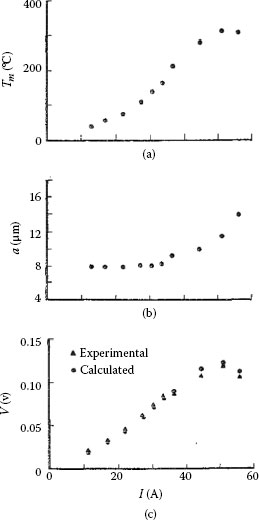
FIGURE 1.70
Dependence on electrical current (large a-spot): (a) Steady state contact temperature Tm (b) Mean radius a of electrical contact and (c) Potential drop V across the contact; note the electrical contact radius a is relatively large, varying from approximately 8 to 14 μm. (From RS Timsit, IEEE Trans Comp Hyb Manuf Tech CHMT-6: 115, 1983 [140].)
In contrast with the data of Figure 1.70, the corresponding data of Figure 1.71 revealed a larger discrepancy between the calculated and measured V values, when the a-spot was approximately 7 nm. In Figure 1.71, note also the calculated contact temperature reached the melting point of aluminum, although there was no physical evidence of melting in the electrical interface. The divergence between experiment and theory illustrated in Figure 1.71 was always observed in aluminum contacts wherever the average a-spot radius was smaller than about 30 nm, that is, wherever the a-spot radius was of the same order of magnitude or smaller than the electronic mean free path [140]. Data of the type illustrated in Figure 1.71 represent clear evidence of a breakdown of classical electrical contact theory for small values of the contact radius a.

FIGURE 1.71
Dependence on electrical current (small a-spot): (a) Steady state contact temperature Tm (b) Mean radius a of electrical contact and (c) Potential drop V across the contact; note that the electrical contact radius a ranges approximately from 7 nm to 10 nm. (From RS Timsit, IEEE Trans Comp Hyb Manuf Tech CHMT-6: 115, 1983 [140].)
1.6.2.1.1 Role of the Sharvin Resistance in Small Aluminum–Aluminum Contacts
The breakdown of classical electrical contact theory revealed in the data of Figure 1.71 stemmed from the ballistic motion of electrons in sufficiently small a-spots, giving rise to the Sharvin resistance, RS. The effect of the Sharvin resistance on the voltage–temperature relation is best investigated by examining the magnitude of the two components in the contact resistance expression Equation 1.57 for aluminum–aluminum contacts. The data of Figure 1.71 indicate that the initial value of a in the contact was approximately 7 nm, which corresponds to a resistance RB of nearly 2 Ω. If the a-spot radius was such that K=lfp/a≈1, then Γ(K)≈0.7 and Equation 1.57 becomes
(1.59) |
If the resistivity of aluminum at room temperature is taken as 2.74 × 10⁻⁸ Ωm [140], the a-spot radius is calculated from Equation 1.59 as 11.9 nm. This is larger than the value of 7 nm evaluated on the basis of classical contact theory as reported in [140]. From Equation 1.59, the Sharvin resistance R2 is immediately evaluated as 1.20 Ω. A current of 0.15 A would be required to generate a voltage drop of 0.3 V across the 2-Ω contact. Although this would be equal to the classical “melting voltage” of aluminum [3,141], melting would not occur since the voltage drop across the “ohmic” component of resistance R1 = 0.80 Ω is only 0.12 V, according to the picture of Figure 1.69. In practice, the voltage drop across R1 would be somewhat larger than 0.12 V since the resistivity would increase due to Joule heating. However, this argument shows melting would not be observed even though the conventional “melting voltage” is reached across the constriction. Note the calculated data of Figure 1.71 obtained for the 2-Ω contact on the basis of classical contact theory, predicted the attainment of the “melting voltage” at a current of 57 mA. This lower value of the current for generating a voltage drop of 0.3 V stems from the effect of contact temperature on the resistivity ρ in a classical contact. The above argument suggests strongly that the disagreement between the experimental and calculated data of Figure 1.71 that is, the apparent breakdown of classical contact theory, stemmed from the absence of consideration of ballistic electronic conduction in classical electrical contact theory.
1.6.3 Observations of Breakdown of Classical Electrical Contact Theory in Gold Contacts
Recently, softening of gold-gold contacts was reported under a contact force near 30 mN where the dimensions of contact asperity were comparable to the electron mean free path lfp at room temperature [193]. It was found that the softening voltage under these conditions was appreciably larger than the value of 80 mV listed Table 1.9, as shown in Figure 1.72. These observations are similar to those associated with the data shown in Figure 1.71 for aluminum contacts. No melting of contact spots was observed even at a voltage drop of 450 mV across the contact, the melting voltage of gold according to classical contact theory ([3] and Table 1.9). The results were explained using a model accounting for ballistic electron transport in the contact.
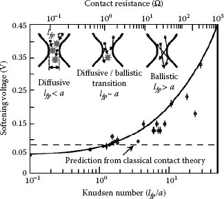
FIGURE 1.72
Measured values of the softening voltage versus the Knudsen Number lfp/a in small gold–gold contacts [193]. As the Knudsen Number increases, electrons pass through the contact spots in a mode ranging from diffusive (classical) to ballistic. The measured softening voltage is compared to the predictions of both a proposed model (solid line) (see [193]) and the classical model (dashed line and Table 1.9; the classical softening voltage was identified as ~ 50 mV in [193] rather than as 80 mV). (From BD Jensen et al., Appl Phys Lett 86: 023507, 2005 [193].)
1.6.4 Observations of Breakdown of Classical Electrical Contact Theory in Tin Contacts
Striking evidence of the breakdown of classical theory was recorded by Maul et al. [194,195,196] from contact intermittencies at a contact load of 0.5 N that is, the observation of large spikes in contact resistance between tin-plated surfaces sliding in reciprocating motion. Contact intermittencies were observed after a number of cycles, thus after the probable growth of relatively thick oxide films on the surfaces due to fretting. Figure 1.73a shows an example of such intermittencies [194] as observed by passage of a current of 54 mA. Note the large voltage spikes of about 0.8 V across the sliding contact, corresponding to an electrical resistance of about 15 Ω. This voltage drop exceeds by far the melting voltage of tin (0.13 V [3] and Table 1.9). The authors reported no physical evidence of contact melting at the locations where this large voltage was detected. In this work, note that the time required to achieve thermal equilibrium in an a-spot (for a as large as 20 μm, see Section 1.4) was on the order of 1 μs. Since the sliding velocity was only 100 μm s−1, the residence time over a single a-spot was considerably longer than 1 μs and thus more than sufficient to cause melting. Thus, sliding did not mitigate melting for the data of Figure 1.73a. Note also that the voltage often could not be sustained above 0. 13 V, thus suggesting that melting had occurred over segments of the sliding path.
It is important to note in Figure 1.73a the resistance of ~ 15 Ω associated with the voltage spikes of 0.8 V could not correspond to conduction through thin tin oxide films. An estimate for the contact resistance Roxide between tin oxide films may easily be made from Equation 1.11 [3]
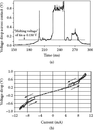
FIGURE 1.73
(a) Intermittencies in a sliding tin–tin contact (b) Voltage–current characteristic at a location of an intermittency in [194]. (From C Maul and JW McBride, Proc 48th IEEE Holm Conf on Elect Cont, 165, 2002 [194].)
Roxide=ρoxide2√πHoxideF
where ρoxide~1 Ωm and Hoxide~9,800 MPa are respectively the resistivity and microhardness of tin oxide [103]. For the contact load F of 0.5 N used by Maul et al. [195], Roxide is evaluated as 1.2 × 10⁵ Ω. Clearly, the voltage spikes could not represent conduction across a tin oxide contact.
Figure 1.73b shows the apparent reproducibility of contact resistance at one location where an intermittency had been detected and sliding had been stopped, in [195]. The direction of electric current across the contact was, then, reversed a few times. The contact resistance was about 43 Ω. Although the data of Figure 1.73b indicate that the “melting voltage” of tin was exceeded, there was no evidence of melting behavior. Melting would have caused irreversible metal flow at a-spots, and would have precluded observations of a stable and reversible voltage–current characteristic. We now interpret the data of Figure 1.73 in terms of the role of the Sharvin resistance.
First we evaluate the Sharvin and “ohmic” components of the resistance. The electronic mean free path for tin at room temperature can be calculated from the resistivity of tin and other physical parameters [188,190] and is evaluated as 4.1 nm. If it is assumed that K ~ 2, then Γ(K) ~ 0.7 so that for the contact resistance of 43 Ω reported in Figure 1.73b, Equation 1.56 reduces to
(1.60) |
For tin ρ = 11.0 × 10⁻⁸ Ωm [188,190]; from which the a-spot radius is immediately evaluated as a = 2.61 nm from a solution of Equation 1.60. Referring to Figure 1.69, the “ohmic” resistance and the Sharvin resistance are evaluated respectively as R1= 14.7 Ω and R2 = 28.3 Ω. In this model, the voltage drop across the temperature-independent Sharvin resistance at the current of 0.008 A in Figure 1.73b is 28.3 × 0.008 = 0.226 V. If the effect of temperature on resistivity is neglected, the residual voltage drop across the ohmic resistance is 14.7 × 0.008 = 0. 118 V, which is slightly below the “melting voltage” of 0.130 V for tin [3,191] and Table 1.9). Thus, no melting should have occurred at the contact spots, and none was observed [194,195,196]. However, the non-linear segment at the ends of the voltage–current curve in Figure 1.73b suggests that the a-spot was getting hot at a current of 0.008 A. This is consistent with the calculated value of the voltage drop across the “ohmic” component of 0.118 V. The proposed model of contact resistance, based on the increasing importance of the Sharvin resistance in small contacts, thus, again provides a rational explanation for the experimental data of Figure 1.73.
1.7 Constriction Resistance at High Frequencies
1.7.1 Skin Depth and Constriction Resistance
Because Equation 1.3 is limited to problems in DC conduction, its validity under conditions of alternating current (AC) is unclear. Holm [3] explored the effect of signal frequency on constriction resistance in a contact geometry similar to that described in [6], but his analysis was only approximate and the results can only be taken as tentative. The major difference between the DC and AC constriction resistance problems stems from the skin effect that occurs under AC conditions. This effect limits the penetration of the electromagnetic field to a depth of a few times the electromagnetic penetration depth δ within a conductor. This penetration depth δ is defined as [4]
(1.61) |
where f is the signal frequency, μ0 is the magnetic permeability of free space (4π × 10−7 H/m) and μr, is the relative permeability of the conductor. In the DC case, constriction resistance is defined as the increase in resistance due to the replacement of a perfectly conducting interface by a constriction as described in Section 1.2. For example, the constriction resistance in a constricted cylinder is defined as the resistance of the constricted cylinder less the resistance of the identical but unconstricted cylinder [6]. Clearly, this definition of constriction resistance is not applicable to conditions of AC excitation, particularly where the frequency is large, since the electric current is concentrated near the conductor surfaces and may also be concentrated near the constriction edges. Extension of the DC definition to the AC case would lead to a situation where the resistance of a given constriction would vary with the specific geometry of the contact interface in which it is located.
With high-frequency AC, the current streamlines are tangential to insulating surfaces, except at a constriction, where the streamlines bend such that the current flow is normal to the contact area, as illustrated in Figure 1.74 [197]. For consistency with the DC case, the definition of constriction resistance at high frequencies is taken as the change in resistance due to the bending of the current streamlines at a circular contact. This resistance will be a function not only of the constriction diameter, but also of the AC excitation frequency and the electrical properties of the conductor. The total connection resistance of an electrical interface will then consist of the sum of (1) The constriction resistance and (2) An additional component stemming from current flow outside the constriction (i.e., from the defined boundary of the external connection). This additional component will obviously be affected by details of the contact geometry. The regions from which these two components of resistance arise are shown as A and B in Figure 1.74.
It is important to recall that the impedance of an electrical interface at high signal frequencies is determined not only by connection resistance, but also by interfacing capacitance and inductance. These latter effects depend on details of the surfaces in contact, such as mechanical contact load and surface roughness, and have been outlined previously [198,199]. They are not addressed in the following description.
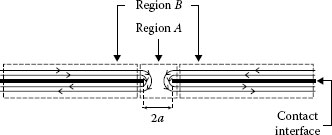
FIGURE 1.74
Schematic diagram of current flow through a circular constriction of diameter 2a at an electrical interface, at high frequencies; flow of electric current occurs within a surface layer determined by the electromagnetic penetration depth, δ. Only the electrical resistance of region A contributes to constriction resistance. The magnitude of the electrical resistance of region B, lying outside of the constriction, depends on the interface dimensions and may contribute significantly to the total connection resistance. (From JD Lavers and RS Timsit, IEEE Trans Comp Packag Tech 25: 446, 2002 [197].)
Table 1.13 lists values of penetration within a non-magnetic material of resistivity 3 × 10⁻⁸ Ωm (e.g. aluminum) for a wide range of frequencies. Typically, the net resistance of a given conductor deviates from the DC value when the penetration depth becomes smaller than the characteristic dimensions of that conductor. For example, consider a constriction with a radius of 100 μm. On the basis of the data shown in Table 1.13, the skin effect will significantly affect the resistance of such a constriction when the AC frequency is higher than 100 kHz. On the other hand, constrictions with a radius of a few to several micrometers will be affected by the penetration depth at frequencies larger than about 10 MHz. Under conditions where the penetration depth is much larger than the constriction radius, the constriction resistance will be described to a good approximation by the classical expression of Equation 1.3.
1.7.2 Evaluation of Constriction Resistance at High Frequencies
The AC constriction resistance has been evaluated numerically for the case of a constricted cylinder of material with resistivity 3 × 10⁻⁸ Ωm using the Finite Element Method (FEM), for constriction radii extending to tens of micrometers and excitation frequencies extending from DC to the GHz range [197]. As anticipated, the skin effect at high frequencies causes the current to be concentrated near conductor surfaces and at insulating boundaries. This concentration is illustrated in Figure 1.75 for the case of a constriction with a/δ ~ 6. Where the skin effect dominates, the entire current is confined to a layer with thickness not more than 5δ. Thus, at high frequencies, current flow to the constriction occurs along the surface defined by the insulating layer in the electrical interface. The current streamlines remain parallel to the insulating layer except to within a distance of 2δ–3δ of the spot edge of the constriction.
TABLE 1.13
Variation of Skin Depth with Frequencyfor a Metal of Resistivity 3 × 10⁻⁸ Ωm
Frequency (Hz) |
Skin Depth δ(μm) |
60 |
11254 |
103 |
2757 |
104 |
872 |
105 |
276 |
106 |
87 |
107 |
28 |
108 |
8.7 |
109 |
2.8 |
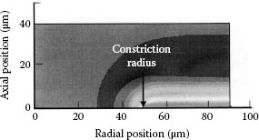
FIGURE 1.75
Illustration of current streamline distribution at 100 MHz in the vicinity of a constriction with radius 50 μm. (From JD Lavers and RS Timsit, IEEE Trans Comp Packag Tech 25: 446, 2002 [197].)
Figure 1.76 shows the calculated current density within a circular constriction of radius a ranging from 5 μm to 50 μm for a current I at a frequency of 10 MHz, 100 MHz and 1 GHz. The current density was normalized to J0 where
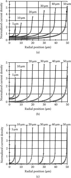
FIGURE 1.76
Current density distribution within constrictions of radius a of 5 μm, 10 μm, 20 μm, 30 μm, 40 μm and 50 μm at an excitation frequency of: (a) 10 MHz (b) 100 MHz (c) 1 GHz; the current density if normalized to I/(2πaδ) where I is the current and δ is the skin depth. (From JD Lavers and RS Timsit, IEEE Trans Comp Packag Tech 25: 446, 2002 [197].)
J0=12πaδ
and δ is given by Equation 1.61. The current concentration at the constriction edge becomes increasingly narrow as the AC frequency increases. The constriction resistance was computed for a constriction radius of 5, 10, 20, 30, 40 and 50 μm, and for frequencies of 10, 100, 1000 MHz. The values of constriction resistance based on this evaluation are shown graphically in Figure 1.77 for the above noted set of parameters. Several features are worth noting. First, the values of constriction resistance converge as the contact radius becomes large. Second, for a given frequency, there is a critical radius ac above which frequency ceases to be a dominating factor in determining the magnitude of the constriction resistance. Third, Figure 1.77 suggests that the critical radius can be linked to the penetration depth δ as follows
aC/δ ≈8
The data of Figure 1.77 indicate clearly that for a selected value of constriction radius, the constriction resistance tends to decrease as the excitation frequency increases. At first glance, this appears to be counterintuitive. However, it must be recalled the constriction resistance describes resistance effects related to the bending of current streamlines in the vicinity of the contact spot. At very high frequencies (constriction radius ≫ skin depth δ), the skin effect dominates and the current flows through to a layer of width ~ δ along the perimeter of the contact spot. It is a mistake to associate this skin depth layer only with electrical resistance since, in the case of a high-frequency contact, the current streamlines must make a transition from a direction tangential to the insulating layer to one normal to the contact area. This transition, characterized by the bending of the streamlines, has an important effect on the net resistance. An analogous situation arises when a DC current flows around a bend as described earlier in Section 1.3.1. With this concept in mind, it becomes clear that at very high frequencies, the streamline pattern, and thus the constriction resistance, becomes relatively independent of frequency; that is, the pattern is set primarily by the radius of the a-spot. Thus, frequency will not have a major impact on constriction resistance at excitation frequencies much larger than 1 GHz. On the other hand, as frequency decreases, a point is reached where the current streamlines occupy more and more of the contact spot. This effect on the streamline pattern appears as an increase in constriction resistance, since the bending of current streamlines occurs over a larger conductor volume. In the lower frequency limit, where the contact radius is much lesser than the skin depth δ, the contact spot tends to throttle current. This, of course, is a case where the constriction resistance is high.
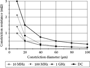
FIGURE 1.77
Dependence of constriction resistanceon constriction radius for excitation frequencies ranging from DC to 1 GHz. (From JD Lavers and RS Timsit, IEEE Trans Comp Packag Tech 25: 446, 2002 [197].)
The DC values of constriction resistance calculated numerically are in exact agreement with the values predicted on the basis of the classical formula ρ/2a (Equation 1.3). The data in Figure 1.77 also indicate that the DC values of constriction provide an upper bound as the frequency decreases to zero. As mentioned earlier, the convergence of results from the DC and AC models takes place at frequencies where the skin effect at the insulating layer no longer is a dominating factor.
1.7.3 Constriction versus Connection Resistance at High Frequencies
The connection resistance of an electrical interface consists of the sum of the resistance of the contact region and the bulk resistance of conductors in the vicinity of the contact that is, at high frequencies, this corresponds to the sum of the resistances of region A and region B in Figure 1.74. It is the parameter usually measured in characterizing the contact properties of electrical junctions. For DC and low-frequency applications, the constriction resistance component of connection resistance is generally much larger than the bulk resistance so the latter component may be neglected. At low frequencies, connection resistance is thus taken as ρ/2a, and is independent of contact geometry. In contrast, connection resistance at high frequencies does depend on geometrical details of the electrical connection, as illustrated below.
Consider the connection resistance, RT at high frequencies of an electrical joint generated by two cylinders of radius Rcylinder, end-butted over a constriction of radius, a, as illustrated in Figure 1.78. The connection resistance measured between location A1 and A2 in Figure 1.78 is
(1.62) |
where RC is the resistance of the constriction of radius a evaluated numerically and Rbulk is the resistance of the bulk material situated between the constriction and each resistance measurement location. Rbulk is the resistance of a ring of thickness given by the penetration depth δ where most of the current flows between the constriction and the cylinder edge. The ring extends from the constriction edge to the edge of the contacting cylinders and its resistance is given as
(1.63) |
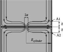
FIGURE 1.78
Two end-butted cylinders passing a high-frequency current.
TABLE 1.14
Dependence of Constriction Resistance and Connection Resistance on Signal Frequency
Signal Frequency f (Hz) |
Constriction Resistance RC (mΩ) |
Connection Resistance RT (Equation 1.62) (mΩ) |
107 |
2.2 |
3.2 |
108 |
1.4 |
4.7 |
109 |
1.0 |
11.2 |
Equations 1.62 and 1.63 indicate the connection resistance of end-butted cylinders at high frequencies increases with the dimension Rcylinder of the contact region, for a fixed constriction radius a. Taken with Equations 1.62 and 1.63, the current streamlines illustrated in Figure 1.78 further indicate that connection resistance increases with increasing frequency although the constriction resistance Rc decreases as the signal frequency increases. These observations are illustrated in Table 1.14 which lists calculated values of Rc and RT for increasing frequencies using parameter values ρ = 3 × 10⁻⁸ Ωm, a = 5 μm, and Rcylinder =100 μm [197].
In Table 1.14, constriction resistance drops by a factor of approximately 2 but the connection resistance RT increases by a factor of 3.5 as the frequency increases from 107 to 109 Hz. As indicated at the beginning of this section, the connection resistance data in Table 1.14 contrast strongly with connection resistance at DC and low frequencies where connection resistance is given by Equation 1.3, independently of the geometry and dimensions of the contact region. The difference in connection resistance properties at high frequencies stems from the skin effect wherein on the one hand less metal is used for electrical conduction, and on the other hand, the bending of current streamlines occurs over a relatively small volume around the constriction, as signal frequency increases.
This chapter has reviewed the origin of electrical contact resistance at solid–solid interfaces and addressed the major factors that affect the fundamental properties of electrical contacts. These factors include surface hardness, the presence of surface contaminants, contact force, and so on, because they affect the dimensions and distribution of a-spots in the electrical interface. Optimization of contact resistance is, thus, generally achieved by optimizing or eliminating selected physical factors through control of surface finishing, the use of relatively soft platings on the contacting surfaces, surface wipe,and so on.
To a good approximation, the true contact area is independent of the nominal contact area in metallic electrical contacts. Also to a good approximation, the true contact area is independent of details of the surface microtopography of the contacting bodies. These observations account for the measured dependence of DC contact resistance on the inverse square root of the contact force. Because electric current is severely constricted in an a-spot, the temperature in an a-spot of the operating contact may be considerably higher than the that of the bodies of the contacting components. The universal parameter determining a-spot temperature is the voltage drop across the electrical interface, not the magnitude of the electric current. Hence, quantities such as softening voltage or melting voltage can be defined for any electrical contact. However, classical electrical contact theory, and hence the voltage–temperature relation, breaks down when the average a-spot diameter is of the same order of magnitude or smaller than the mean free path of conduction of electrons in the contacting bodies. Under these conditions, electrons behave ballistically in a-spots and a-spot temperature cannot be calculated readily from the voltage drop across the contact.
Operation of a bimetallic electrical contact at consistently elevated a-spot temperatures may generate high-resistivity intermetallic compounds in the interface. Formation of these compounds is generally detrimental to contact stability and may eventually lead to contact failure.
Capillarity and thermally induced material flow within a small a-spot can have significant effects on the constriction resistance of an electrical interface. These effects are generally responsible for so-called “self-healing” in electrical contacts, that is, when the area of metal-to-metal contact increases due to Joule heating, thus decreasing contact resistance. These effects generally occur when the a-spot temperature reaches the softening temperature. They have been observed at room temperature in sufficiently small a-spots where sintering occurs.
At sufficiently high signal frequencies, constriction resistance decreases with increasing excitation frequency. This effect may be understood as follows: under DC or low-frequency conditions, the presence of a constriction at an electrical interface causes spreading of current streamlines in the immediate vicinity of the constriction. Spreading effectively increases the length of current pathways in the conductors and thus increases the resistance to electrical flow. This increase is effectively responsible for constriction resistance. At sufficiently high frequencies, current is confined near the constriction edge and near the surfaces in contact due to the skin effect. This confinement diminishes the spreading of current streamlines within the conductors and shortens the electric current pathways near the constriction. This leads to an effective decrease in constriction resistance.
The author thanks Drs Irvin H. Brockman and Robert S. Mroczkowski of AMP Incorporated (now TE Connectivity Ltd), for having supplied much of the contact resistance data associated with electroplated layers and for helpful discussions during the preparation of the first version this chapter published in this book in 1999. Much of this information has again been used in this updated version of the chapter. The author is also grateful to Dr J.B.P. Williamson for discussing details of the work described in reference 56.
Appendix 1.A Electrical Resistivity and Thermal Conductivity of Metals and the Wiedemann–Franz Law
The simple derivation of the Wiedemann–Franz law presented in this appendix requires a brief review of quantum mechanical properties of electrons in solids.
Electrons in a metal occupy a large but finite number of quantum energy states. The number of these states, ranging in energy from zero to E, is given as [188]
(1.A.1) |
where V is the metal specimen volume, m is the mass of the electron and h is Planck’s constant. At a temperature of 0 K, the first electron will be located in the lowest energy state and subsequent electrons will occupy higher energy states. If there are N electrons in the metal sample, the number of states described by F(E) becomes identical with N and the maximum electron energy Emax calculated from Equation 1.A.1 is given as
(1.A_2) |
For metals such as copper and aluminum, the electrons associated with each atom are arranged in closed shells with the outer shell carrying respectively one electron and three electrons. In the solid state, it is these outer shell electrons that detach themselves from the atoms and act as the “free” electrons responsible for the electrical conductivity of the metals. Since one mole of any element contains 6.02 × 10²³ atoms (Avogadro’s number) and the densities of copper and aluminum are respectively 8.9 g cm−3and 2.7 g cm−3, the density of free electrons in copper and aluminum is respectively 8.4 × 1028 and 5.0× 1028 electrons per cubic meter. Substituting these values for the density N/V in Equation 1.A.2 yields a maximum electronic energy of 1.12 × 10⁻¹⁸J (~7 eV) and 8.2 × 10⁻¹⁹ J (~ 5 eV) respectively for copper and aluminum. These energies are considerably larger than the energy 3kT/2, where k is Boltzmann’s constant, associated with the motion of classical particles at room temperature, since this energy is only ~ 6.2 × 10⁻²¹ J (~ 0.04 eV). This is the reason why classical physics cannot be used to treat the electrical conductivity of metals. If the electronic energy Emax is equated to the kinetic energy mv2/2, the velocity of electrons in metals is ~ 106 ms−1 and is, thus, much larger than the velocity of ~ 105 ms−1 for classical particles at room temperature.
From Equation 1.A.1, the density of states f(E)per unit energy interval obtained by differentiating with respect to E is given as
(1.A.3) |
and the distribution has a parabolic dependence on E. At 0 K, this distribution has a sharp cut-off at an energy value defined by Emax(~5−7 eV) as illustrated in Figure 1.A.1a, since no free electron can have an energy larger than this. Now, the probability that an electron has an energy E at a temperature T is given by the Fermi–Dirac distribution function fFD(E) defined as [188]
(1.A.4) |
where EF is defined as the Fermi energy. Inspection of expression in Equation 1.A.4 indicates that fFD(E) is unity at 0 K for values of E up to EF, and is equal to zero for E > EF as shown in Figure 1.A.1b. Since the maximum electron energy at 0K is Emax, it follows that EF=Emax at 0K. Generally, the Fermi energy varies with temperature and its value is calculated by equating the total number of occupied states to the actual number of free electrons [188]. In metals, it is usually sufficient to ignore this dependence on temperature and assume that EF is always equal to is Emax. The density of states accessible to electrons may now be calculated. From Equations 1.A.3 and 1.A.4, the number of states lying between energies E and E + dE and occupied by electrons at any temperature is
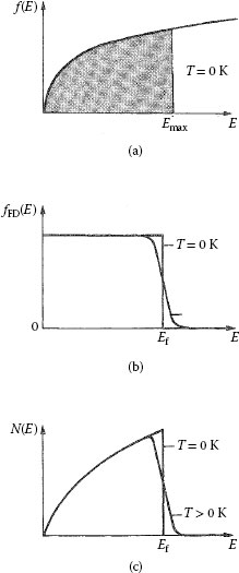
FIGURE 1.A.1
Dependence of the density of states f(E) on energy for the free electron model: (a) At OK, all the states with energy up to Emax are occupied. (b) The Fermi–Dirac function fFD(E) (c) Density of occupied electronic states N(E)=f(E)fFD(E).
(1.A.5) |
so that the density of occupied electronic states N(E) given as f(E)fFD(E) varies with E as shown in Figure 1.A.1c. Note that at 0 K, the function N(E) has a parabolic form with a sharp cut-off at EF. As the temperature is raised, the energy distribution becomes slightly rounded at the cut-off and acquires a thin tail extending to higher energies. The physical significance of this change in energy distribution is that only electrons with energies near EF=Emax can change their state by absorption of thermal energy as this energy of order kT and is thus too small to excite electrons with energies significantly lower than EF. The electronic specific heat may, then, be calculated by assuming that only those electrons within the thermal energy ~ kT of EF can absorb energy as the temperature is raised. The actual number of electrons involved will then be the density of states N(EF) at EF multiplied by kT that is, N(EF)kT, and the total energy absorbed will thus be N(EF)(kT)2. The electronic specific heat ce, is then, obtained by differentiating this absorbed energy with respect to T, or
ce~2N(EF)k2T
The more accurate expression obtained by differentiating the integrated Expression 1.A.5 with respect to T yields [188]
(1.A.6) |
Now, the classical kinetic theory of gases relates the thermal conductivity λ and the specific heat per unit volume cv as [200]
λ=cvlfpv3
where v is the average molecular speed and lfp is the mean free path between molecular collisions. In analogy, and using Equation 1.A.6, the specific heat of an electron gas in a metal may then be written as
(1.A.7) |
The electrical resistivity ρ may be related to fundamental electronic properties also by evoking the arguments in classical physics. Under the action of an electric field Eel, the electric current density j generated is given as
(1.A.8) |
where n is the electron density defined earlier as N/V, e is the electronic charge and vd is the electron drift velocity. Now, the electric force acting on each electron is eEel and this is approximately equal to mvd/τ where τ is the mean time between collisions with atoms and m is the electronic mass, so that
(1.A.9) |
Since τ−1 is given as vF/lfp and vF is defined as [2EF/m]1/2, Equations 1.A.8 and 1.A.9 immediately give
j=Eelne2lfpmvF
or, since j is also given as Eel/ρ where ρ is the electrical resistivity,
(1.A.10) |
Combining Equations 1.A.7 and 1.A.10 and using the fact that mv2F~2EF yields
(1.A.11) |
Equation 1.A.11 is a statement of the Wiedemann–Franz law.
The Wiedemann–Franz law was derived on the assumption that the electrical and thermal conductivities are determined by the same mean free path lfp for collisions of the conduction electrons with the solid matrix. In practice, the thermal energy lost by electron collisions with the lattice is conducted by vibrating atoms in the solid. Hence, these collisions are somewhat more disruptive to thermal transfer by electrons than to electrical conduction. The effective mean free paths associated with electrical and thermal transport are, thus, not rigorously identical, with the consequence that the Wiedemann–Franz law is often not strictly valid. Deviations are most evident in the low-temperature regime (< 200 K) where scattering of conduction electrons by impurities becomes important [188,200]. In the room temperature regime and at more elevated temperatures, the Wiedemann–Franz law holds reasonably well for a wide variety of metals [188,200].
Appendix 1.B
Location of the Plane of Maximum Temperature in a Bimetallic Contact
Consider the circular spot in Figure 1.B.l involving materials 1 and 2 in which the electrical resistivities are such that ρ1 < ρ2. The maximum temperature Tm is assumed to occur in a surface located in material 2 at a distance Δz from the physical interface. The physical interface is assumed to be isothermal at a temperature Tj. If the a-spot is circular and the electric current passed through the contact is I, the electric power Δz generated within the element of thickness Δz is given approximately as
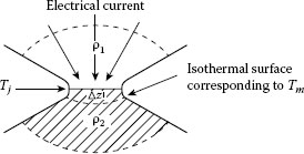
FIGURE 1.B.1
Schematic representation of isothermal surfaces in a joule-heated bimetallic interface in which the resistivities are such that ρ2 > ρ1.
ΔP≈ρ2,mΔzπa2I2
where ρ2,m is the electrical resistivity of material 2 at the maximum temperature Tm. If the thermal conductivity of material 2 at the maximum temperature is λ,2,m, the rate of heat loss ΔW to material 1 from this disk is approximately
ΔW≈λ2,m{Tm−Tj}πa2Δz
At thermal equilibrium,ΔP=ΔW, yielding
(1.B.1) |
Now from Equation 1.34, the potential drop ΔV between the physical interface and the plane of maximum temperature is related to the temperature difference (Tm – Tj) as
(1.B.2) |
Also, the current I is related to the total voltage drop V across the contact by the approximate relation
(1.B_3) |
Substituting Equations 1.B.2 and 1.B.3 into Equation 1.B.1 yields
Δza=ρ2,m+ρ1,m2ρ2,mΔVVπ2√2
For the sake of illustration, ifρ2,m=3ρ1,m and ΔV/V takes on the large value of 0.1 (ΔV/V would be expected to be considerably smaller than this), Δz/a would be of the order of 0.07. Thus for an a-spot of radius 10 μm, Δz would be displaced only approximately 700 nm from the physical interface, into the material of larger resistivity. If the highly conductive material is aluminum with ρl,m=5.5×10⁻⁸ Ωm at a maximum contact temperature of approximately 400°C (ρ2,m=1.65×10⁻⁷ Ωm), using λ2,m = 200 Wm−1K−1 and V ~ 0.2V (or ΔV = 0.02V), Equation 1.B.1 yields a difference between the temperature of the physical interface and the maximum contact temperature of only about 6°C! For all practical purposes, the maximum temperature may be considered to occur at the physical interface. However, the detailed temperature distribution within the contact region is not identical to that described by Equation 1.45 for the monometallic contact, and must be worked out on the basis of Equations 1.33 and 1.41.
Appendix 1.C Location of the Plane of Maximum Temperature in an Electrical Contact Consisting of Mating Components of Greatly Differing Electrical Resistivities
The surface at which the maximum temperature is reached in a contact consisting of mating components of vastly differing electrical resistivities would be expected to be located in the material with higher resistivity. The location of this surface may be estimated for the simple case where the contact is two-dimensional, as illustrated in Figure 1.C.l.
The contact is assumed to consist of two two-dimensional pyramids in contact over an area 2al, where 2a is the width of the contact in the y-direction and l is the junction thickness. The pyramids meet at x = 0 and extend to the left and right of the y-axis by a distance L. The pyramid edges diverge from parallelism by an angle φ and are assumed to be thermally insulated. For the sake of simplicity, the resistivities ρ1, ρ2 and the thermal conductivities λ1, λ2 of the two materials are assumed to be independent of temperature. The equations describing the steady-state heat generation are given as
(1.C.1) |
and
(1.C.2) |
Since the cross-sectional area of the pyramid is 2al(1+[x/a]tanφ), where x > 0 is the distance from the origin, the current density function may be approximated as
j(x)=j01+{xa}tanφ, x>0 j(x)=j01−{xa}tanφ, x<0
where j0 is the current density at x = 0. Note that this current density distribution is only approximate since there cannot be an abrupt change in the direction of current flow at x = 0. Also, this current distribution cannot be valid as φ approaches π/2. Substitution of these current density distributions into Equations 1.C.1 and 1.C.2 immediately yields the following solutions for the temperature distributions:
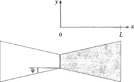
FIGURE 1.C.1
Two-dimensional electrical contact consisting of two two-dimensional pyramids touching over an area 2al, where 2a is the width of the contact in the y-direction and l is the junction thickness. The pyramids meet at x = 0 and extend to the left and right of the y-axis by a distance L The pyramid edges diverge from parallelism by an angle φ and are assumed to be thermally insulated.
T1(x)=ρ1λ1{aj0tanφ}2ln{1−xatanφ}+B1x+C1, x<0
T2(x)=ρ2λ2{aj0tanφ}2ln{1−xatanφ}+B2x+C2, x>0
where B and C are integration constants determined by the following boundary conditions:
λ1d2T{x}dx=λ2d2T{x}dx at x=0
T1{0}=T2{0}
T1(−L)=T2(L)=T0
These boundary conditions immediately yield the following expressions for the constants B1, B2, C1, and C2:
B1=aj20{λ1+λ2}tanφ(ρ1+ρ2−aλ2Ltanφ{ρ2λ2−ρ1λ1}ln{1+tanφLa})
B2=−aj20{λ1+λ2}tanφ(ρ1+ρ2+aλ1Ltanφ{ρ2λ2−ρ1λ1}ln{1+tanφLa})
C1 = C2=T0−ρ2λ2{aj0tanφ}2ln{1+tanφLa}−B2L
If it is assumed that ρ2 ≫ ρ1 then the isothermal surface associated with the maximum temperature is located in material 2. In this case, the condition dT2(x)/dx=0 yields the location of the temperature maximum as
(1.C.3) |
Thus, the location of the isothermal surface corresponding to the maximum temperature is sensitive to the inclination of the contacting asperities generating the a-spot. It may easily be shown that the voltage drop across the contact is given as
V=aj0tanφ{ρ1+ρ2}ln{1+tanφLa}
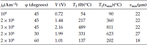
For a copper–graphite contact where λ1 ~ 380 Wm−1°C−1 and ρ1= 2.6 × 10⁻⁸ Ω m, λ2 ~ 40Wm−1°C−1 and ρ2 = 0.003 Ωm, the calculated steady-state temperature distribution for the following values of contact parameters j0 = 2 × 10⁸ Am−2, L = 100 μm, a = 10μm and φ=π/4 is shown in Figure 1.C.2. Note the maximum temperature of 360°C occurs at a distance of 22 μm from the copper–graphite interface where the temperature is 217°C. Table l.C.1 illustrates the dependence of interface temperature, maximum temperature and the location xmax from the copper–graphite interface of the isothermal plane at the maximum temperature, on such factors as the current density and the asperity angle φ. Note the maximum temperature within the graphite occurs at a relatively large distance from the copper–graphite interface. Also, in all the cases discussed, the maximum temperature is significantly higher than that of the interface.
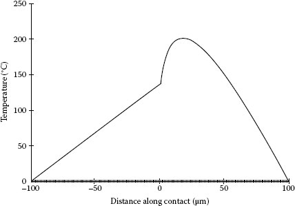
FIGURE 1.C.2
Calculated steady state temperature distribution for a two-dimensional copper–graphite contact of the geometry illustrated in Figure 1.C.1 where λ1 ~ 380 Wm−1°C−1, ρ1 = 2.6 × 10⁻⁸ Ω m, λ2 ~ 40 Wm−1oC−1 and ρ2 = 0.003 Ωm, for the following values of con tact parameters: j0 = 2 × 10⁸ Am−2, L = 100 μm, a = 10 μm, and φ = π/4.
TABLE 1.C.1
Dependence of xmax, T2(0), T2(xmax), and Voltage-Drop V Across the Copper–Graphite Contact on the Current Density j0 and the Asperity Angle φ for L = 100 μm and a = 10 μm
1. TR Thomas, Rough Surfaces, New York: Longman, 1982.
2. JA Greenwood and JBP Williamson, Contact of nominally flat surfaces, Proc Roy Soc A295: 300, 1966.
3. R Holm, Electric Contacts, Theory and Applications, Berlin: Springer–Verlag, 2000.
4. WR Smythe, Static and Dynamic Electricity, New York: McGraw-Hill, 1968.
5. RS Timsit, The potential distribution in a constricted cylinder, J Phys D Appl Phys 10: 2011, 1977.
6. AM Rosenfeld and RS Timsit, The potential distribution in a constricted cylinder: An exact solution, Quart Appl Math 39: 405, 1981.
7. RS Timsit, The potential distribution in a constricted cylinder, Proc 14th Int Conf Elect Cont, Paris, 21, 1988.
8. H Aichi and N Tahara, Analysis on the constriction resistance of the electric contact by the contact model using the electrolyte bath, Proc. 20th Int Conf Elect Cont, Nagoya, Japan, 1, 1994.
9. M Nakamura, Constriction resistance of conducting spots by the boundary element method, IEEE Trans Comp Hyb Manuf Tech, CHMT-16: 339, 1993.
10. TR Thomas and SD Probert, Establishment of contact parameters from surface profiles, J Phys D: Appl Phys 3: 277, 1970.
11. JA Greenwood, Constriction resistance and the real area of contact, Brit J Appl Phys 17: 1621, 1966.
12. M Nakamura and I Minowa, Computer simulation for the conductance of a contact interface, IEEE Trans Comp Hyb Manuf Tech CHMT-9: 150, 1986.
13. I Minowa, M Nakamura, and M Kanno, Conductance of a contact interface depending on the location and distribution of conducting spots, Proc Elect Conf Cont, Electromech Comp Appl, 19, 1986.
14. JF Archard, Single contacts and multiple encounters, J Appl Phys 32: 1420, 1961.
15. FP Bowden and D Tabor, Friction and Lubrication of Solids, Vol. II, Oxford: Oxford University Press, 1964.
16. A Fairweather, The closure and partial separation of an electric contact, IEE (London) 92: 301, 1945.
17. EL Shobert, Calculation of electrical contacts under ideal conditions, Proc ASTM 46: 1126, 1946.
18. P Barkan and EJ Tuohy, A contact resistance theory for rough hemispherical silver contacts in air and in vacuum, IEEE Trans Power App Sys 84: 1132, 1965.
19. DV Keller, Electric contact phenomena in ultra clean and specifically contaminated systems, Proc. Holm Seminar on Electrical Contact Phenomena, (18th Holm Conf Elect Cont), Chicago, IL, 1, 1971.
20. RE Cuthrell and DW Tipping, Electric contacts II: Mechanics of closure for gold contacts, J Appl Phys 44: 4360, 1973.
21. JB Pethica and D Tabor, Characterized metal microcontacts, J Adhes 13: 215, 1982.
22. Y Watanabe, New instrument for measuring contact resistance developed for studying electrical contact phenomena, Wear 112: 1, 1986.
23. LP Solos, An approach to predicting wear and friction in contact design, Elect Cont-1962: Eng Sem Elect Cont, University of Maine, June 1962.
24. SW Park and SJ Na, Contact pressure and current density distribution in a circular contact surface, IEEE Trans Comp Hyb Manuf Tech CHMT-13: 320, 1990.
25. Y Sano, Effect of space angle on constriction resistance and contact resistance for a point contact, J Appl Phys 58: 2651, 1985.
26. RS Timsit, Constriction resistance of thin film contacts, IEEE Trans Comp Pack Tech 33: 636, 2010.
27. G Norberg, S Dejanovic and H Hesselbom, Contact resistance of thin metal film contacts, IEEE Trans Elect Dev 29: 371, 2006.
28. P Zhang and YY Lau, Scaling laws for electrical contact resistance with dissimilar materials, J Appl Phys 108: 044914, 2010.
29. P Zhang, YY Lau and RM Gilgenbach, Minimization of thin film contact resistance, Appl Phys Lett 97: 204103, 2010.
30. P Zhang, YY Lau and RM Gilgenbach, Thin film contact resistance with dissimilar materials, J Appl Phys 109: 124910, 2011.
31. P Zhang, YY Lau, and RS Timsit, On the spreading resistance of thin metal film contacts, IEEE Trans Comp Pack Tech 39: 1936, 2012.
32. PM Hall, Resistance calculations for thin film patterns, Thin Solid Films 1: 277, 1967.
33. PM Hall, Resistance calculations for thin film rectangles, Thin Solid Films 300: 256, 1997.
34. JA Greenwood and JBP Williamson, Electrical conduction in solids II: Theory of temperature-dependent conductors, Proc Roy Soc A246: 13, 1958.
35. DK Schroder, Semiconductor Material and Device Characterization, New York: Wiley, 149, 1998.
36. HH Berger, Models for contacts to planar devices, Solid State Elect 15: 145, 1972.
37. S Kristiansson, F Ingvarson, and KO Jeppson, Compact spreading resistance model for rectangular contacts on uniform and epitaxial substrates, IEEE Trans Elect Devices 54: 2531, 2007.
38. A Nussbaum, Capacitance and spreading resistance of a stripe line, Solid State Elect 38: 1253, 1995.
39. MS Leong, SC Choo, and LS Tan, The role of source boundary condition in spreading resistance calculations, Solid State Elect 21: 933, 1978.
40. RH Cox, H Strack, Ohmic contacts for Ga–As devices, Solid State Elect 10: 1213, 1967.
41. B Gelmont and M Shur, Spreading resistance of a round ohmic contact, Solid State Elect 36: 143, 1993.
42. MW Denhoff, An accurate calculation of spreading Resistance, J Phys D Appl Phys 39: 1761, 2006.
43. MB Read, JH Lang, AH Slocum, and R Martens, Contact resistance of flat-on-flat and sphere-on-flat thin films, Proc 56th IEEE Holm Conf on Elect Cont jointly with 25th Int Conf Elect Cont, Charleston, SC, 348, 2010.
44. MB Read, JH Lang, AH Slocum, and R Martens, Contact resistance in flat thin films, Proc 55th IEEE Holm Conf on Elect Cont, Vancouver, BC, Canada, 300, 2009.
45. S Sawada, S Tsukiji, S Shimada, T Tamai, and Y Hattori, Current density analysis of thin film effect in contact area on LED wafer, Proc 58th IEEE Holm Conf Elect Cont, Portland, OR, 242, 2012.
46. PF Preston, An industrial atmosphere corrosion test for electrical contacts and connections, Trans Inst Met Fin 50: 125, 1972.
47. RG Baker, Studies of static low voltage contacts at the Bell Telephone Laboratories, Proc 2nd Int Symp Elect Cont Phen, Graz, Austria, 545, 1964.
48. HW Hermance and TF Egan, Organic deposits on precious metal contacts, Bell Syst Tech J, 37: 739, 1958.
49. M. Antler, M Feder, CF Hornig, and J Bohland, The corrosion behaviour of single and multiphase tin-nickel alloy electrodeposits, Plating and Surface Finishing, 63: 30, 1976.
50. TR Long and KF Bradford, Contact resistance behaviour of the 60Pd40Ag alloy in tarnishing environments, Proc. Holm Sem Elect Cont, Illinois Institute of Technology, Chicago, IL, 145, 1975.
51. M Antler, MH Drozdowicz, and CF Hornig, The corrosion resistance of worn tin-nickel and gold-coated tin-nickel alloy electrodeposits, J Electrochem Soc 124: 1069, 1977.
52. M Antler, Contact resistance of tin-nickel electrodeposits, J Electrochem Soc 125: 420, 1978.
53. M Antler, MH Drozdowicz, and CA Haque, Connector contact materials: effect of environment on clad palladium, palladium-silver alloys, and gold electrodeposits, IEEE Trans Comp Hyb Manuf Tech CHMT-4: 482, 1981.
54. M Braunovic, Fretting damage in tin-plated aluminum and copper connections, Proc of Electric Contacts-1988, IEEE-Holm, San Francisco, CA, 179, 1988.
55. M. Nakamura and I Minowa, Film resistance and constriction effect of current in a contact interface, IEEE Trans Comp Hyb Manuf Tech CHMT-12: 109, 1989.
56. JBP Williamson and JA Greenwood, The constriction resistance between electroplated surfaces, Proc Int Conf Elect Cont Electromech Comp, Appendix, Beijing, China, Oxford: Pergamon Press, 1989.
57. G Horn, Test method for cleanliness of technical contact surfaces by an automatic measurement device for contact resistance, Proc. 8th Int ConfElect Cont Phen, Tokyo, Japan, 499, 1976.
58. MP Asar, FG Sheeler, and HL Maddox, Measuring contact contamination automatically, Western Electric Engineer 23: 32, 1979.
59. ASTM B667-80, American Society for Testing Materials, Philadelphia.
60. MR Pinnel and KF Bradford, Influence of some geometric factors on contact resistance probe measurements, Proc 28th Elect Comp Conf, Anaheim, CA, 129, 1978.
61. J King, High-pressure electrical contacts, Proc Elect Comp Conf, Washington, DC, 454, 1968.
62. M Antler, WF Graddick, and HG Tompkins, Base metal contacts: An exploratory study of separable connection to tin-lead, IEEE Trans Parts Hyb Packag PHP-IF: 35, 1975.
63. CL Bauer and GG Lessman, Metal joining methods, Annu Rev Mater Sci 6: 361, 1976.
64. ER Wallach and GJ Davis, Mechanical properties of aluminum–copper solid-phase welds, Metals Tech, April, 183, 1977.
65. JA Rayne and CL Bauer, Effect of intermetallic phase formation on electrical and mechanical properties of flash-welded Al–Cu couples, Proc 5th Bolton Landing Conf Weld, Phy Metall Fail Pheno, General Electric Co., Schenectady, NY, 353, 1979.
66. JA Rayne, MP Shearer, and CL Bauer, Investigation of interfacing reactions in thin film couples of aluminum and copper by measurement of low temperature contact resistance, Thin Solid Films 65: 381, 1980.
67. ER Wallach and GJ Davis, Joint resistance and current paths in heat-treated aluminum–copper solid-state welds, Metals Sci 11: 97, 1977.
68. AW Urquhart, Interdiffusion studies on contact plating materials, Holm Seminar on Electrical Contacts, Illinois Institute of Technology, Chicago, IL, 185, 1976.
69. DA Unsworth and CA Mackay, A preliminary report on growth of compound layers on various metal bases plated with tin and its alloys, Trans Inst Metal Finish 51: 85, 1973.
70. RS Timsit. Intermetallics growth at Al–α-brass interfaces, Acta Met 33: 97, 1985.
71. RS Timsit. Interdiffusion at bimetallic interfaces, IEEE Trans Comp Hyb Manuf Tech CHMT-9: 106, 1986.
72. M. Braunovic and N Alexandrov, Intermetallic compounds at aluminum-to-copper electrical interfaces: Effect of temperature and electric current, IEEE Trans CompPack Manuf Tech CHMT-A17: 78, 1994.
73. V Simic and Z Marinkovic, Review: Room temperature reactions in thin metal couples, J Mat Sci 33: 561, 1998.
74. M Abbasi, A Karimi Taheri, and MT Salehi, Growth rate of intermetallic compounds in Al–Cu bimetal produced by cold roll welding process, J Alloy Comp 319: 233, 2001.
75. KN Tu, Interdiffusion in thin films, Ann Rev Mater Sci 15: 147, 1985.
76. FM D’Heurle and PS Ho, Electromigration in Thin Films: Interdiffusion and Reactions, (eds) J.M., Poate, KM Tu, and JM Mayer, New York: Wiley, 243, 1978.
77. KN Tu, Recent advances on electromigration in very–large-scale integration of interconnects, J Appl Phys 94: 5451, 2003.
78. U Gosele and KN Tu, Growth kinetics of planar binary diffusion couples: Thin-film case versus bulk cases, J Appl Phys 53: 3252, 1982.
79. D Gupta and PS Ho, Diffusion processes in thin films, Thin Solid Films 72: 399, 1980.
80. RS Timsit, The connectibility properties of aluminum: Contact fundamentals, Can Elect Assoc Rep 76-19, 1976.
81. DM Rabkin, VR Ryabov, AV Lozovskaya, and VA Dovzhenko, Preparation and properties of copper—aluminum intermetallic compounds, Sov Powd Met Metal Ceram 8: 695, 1970.
82. M Braunovic and N Alexandrov, Intermetallic compounds at aluminum-to-copper and copper-to-tin electrical interfaces, Proc 38th Holm Conf Elect Cont, Philadelphia, PA, 25, 1992.
83. JT Wilson, Report of the Commission of Inquiry on Aluminum Wiring, Queen’s Printer for Ontario, Part 2, Ontario, Canada, March 22, 1979.
84. PE Tegehall, Review of the impact of intermetallic layers on the brittleness of tin-lead and lead-free solder joints, IVF Project Report 06/07, IVF Industrial Research and Development Corporation, SE-431, 53 Moldal, Sweden, 2006 (available on the internet at http://extra.ivf.se/eqs/dokument/7%20pet6005.pdf).
85. CD Breach and FW Wulff, A brief review of selected aspects of the materials science of ball bonding, Microelectron Reliab 50: 1, 2010.
86. G Zeng, S McDonald, and K Nogita, Development of high temperature solders: review, Microelectron Reliab 52: 1306, 2012.
87. RJK Wassink, Soldering in Electronics, Scotland: Electrochemical Publications, p. 99, 1984.
88. GA DiBari, Nickel Electroplating for engineering electroforming and decorative purposes, Plating and Surface Finishing 70: 24, 1983.
89. D Olsen, R Wright, and H Berg, Effects of intermetallics on the reliability of tin-coated Cu, Ag and Ni parts, Proc 13th Ann Reliab Phy Symp, Las Vegas, NV, 80, 1975.
90. PJ Kay and CA Mackay, Barrier layers against diffusion, Trans Inst Metal Finishing 57: 169, 1979.
91. TK Do, A Lund, A reliability study of new nanocrystalline nickel alloy barrier layer for electrical contacts, Proc 56th IEEE Holm Conf. Electrical Contacts and 25th Int Conf Elect Cont, Charleston, SC, 73, 2010.
92. MA Nicolet, Diffusion barriers in thin films, Thin Solid Films 52: 415, 1978.
93. B Chudnovsky, V Pavageau, and M Rapeaux, The quality of tin plating on aluminum exposed to elevated temperatures: The role of underplating, Proc 24th Int Conf Elect Cont, Saint-Malo, France, 495, 2008.
94. M Runde, E Hodne, and B Tøtdal, Experimental study of the conducting spots in aluminum contact interfaces, IEEE Trans Comp Hyb Manuf Tech 13: 1068, 1990.
95. C Ruppert and M Runde, Thermally induced mechanical degradation of contact spots in aluminum interfaces, IEEE Trans Comp Pack Tech 29: 833, 2006.
96. HB Huntington, Electro- and thermomigration in metals, In: Diffusion, Proc 1972 Seminar of the ASM, American Society of Metals, 1973, p. 155.
97. H Gan and KN Tu, Polarity effect of electromigration on kinetics of intermetallic compound formation in Pb-free solder V-groove samples, J Appl Phys 97: 063514, 2005.
98. RJ Osias and JH Tripp, Mechanical disruption of surface films on metals, Wear 9: 388, 1966.
99. RS Timsit, Some fundamental properties of aluminum-aluminum electrical contacts, IEEE Trans Comp Hyb Manuf Tech 3: 71, 1980.
100. A Ronnquist and H Fischmeister, The oxidation of copper, J Inst Metals 89: 65 1960.
101. MG Hapase, MK Gharpurey, and AB Biswas, The oxidation of vacuum deposited films of copper, Surf Sci 9: 87, 1968.
102. W Campbell and UB Thomas, The oxidation of metals. Trans Electrochem Soc 91: 623, 1947.
103. GV Samsonov, The Oxide Handbook, New York: Plenum Press, 1973.
104. JS Anderson and NN Greenwood, The semiconducting properties of cuprous oxide, Proc Roy Soc A215: 353, 1952.
105. G. Honjo, Electron diffraction studies on oxide films formed on metals and alloys, Part 1: Oxidation of pure copper, J Phy Soc Japan 4: 330, 1949.
106. G Honjo, Electron diffraction studies on oxide films formed on metals and alloys, Part 2: Selective oxidation of alloys, J Phy Soc Japan 8: 113, 1953.
107. KR Lawless and AT Gwathmey, The structure of oxide films on different faces of a single crystal of copper, Acta Met 4: 153, 1956.
108. EG Clarke and AW Czanderna, Optical transmittance and microgravimetric studies of the oxidation of < 100 > single crystal of copper, Surf Sci 49: 529, 1975.
109. M Batzill and U Diebold, The surface and materials science of tin oxide, Prog Surf Sci 79: 47, 2005.
110. U Kuxmann and R Dobner, Untersuchungen im system zinn-zinn(IV)-oxid im temperaturbereich der mischungslucke, Metallwissenschaft und Technik 34: 821, 1980.
111. JH Lee and SJ Park, Temperature dependence of electrical conductivity in polycrystalline tin oxide, J Am Ceram Soc 73: 2771, 1990.
112. T Tamai, S Sawada, and Y Hattori, Deformation of crystal structure and distribution of mechanical stress in tin-plated layer under contact loading, Proc 55th Holm Conf Elect Cont, Vancouver, 160, 2009.
113. Y Nabeta, Y Saitoh, S Sawada, Y Hattori, and T Tamai, Growth law of the oxide film formed on the tin plated contact surface and its contact resistance characteristic, Proc 55th Holm Conf Elect Cont, Vancouver, 174, 2009.
114. T Tamai, Y Nabeta, S Sawada, and Y Hattori, Property of tin oxide film formed on tin-plated connector contacts, Proc 56th Holm Conf Elect Cont and 25th Int Conf Elect Cont, Charleston, SC, 295, 2010.
115. EI Alessandrini, Effect of temperature and environment on the structure of thin single-crystal nickel oxide films, J Appl Phys 35: 1606, 1964.
116. SH Kulpa and RP Frankenthal, Tarnishing of nickel in air at temperatures from 23°C to 200°C and relative humidities from ambient to 95%. %, J Electrochem Soc 124: 1588, 1977.
117. MJ Graham and M Cohen, On the mechanism of low-temperature oxidation (23°C-450°C) of polycrystalline nickel, J Electrochem Soc 119: 879, 1972.
118. I Fasaki, A Koutoulaki, M Kompitsas, and C Charitidis, Structural, electrical and mechanical properties of NiO thin films grown by pulsed laser deposition, Appl Surf Sci 257: 429, 2010.
119. H van Oosterhout, Evaluation of electroplated nickel phosphorous with high phosphorous content, AMP J Techn 2: 63, 1992.
120. WE Campbell, Lectures on tarnishing, friction and wear in electrical contacts, given at the Sym Elect Cont, Pennsylvania State University, 1956.
121. P Vassiliou and CT Dervos, Corrosion effects on the electrical performance of silver metal contacts, Anticorros Meth M46: 85, 1999.
122. RV Chiarenzelli, Tarnishing studies on contact materials, IEEE Trans PartsMat Packag 3: 89, 1967.
123. WH Abbott, Effects of industrial air pollutants on electrical contact materials, IEEE Trans Parts Hyb Packag 10: 24, 1974.
124. J Guinement and C Fiaud, Laboratory study of the reaction of silver and copper with some atmospheric pollutants: Comparison with indoor exposition of these materials, Proc 13th Int Conf Elect Cont, Lausanne, 383, 1986.
125. H Kim, Corrosion process of silver in environments containing 0.1 ppm H2S and 1.2 ppm NO2, Mater Corros 54: 243, 2003.
126. MH Hebb, Electrical conductivity of silver sulfide, J Chem Phys 20: 185, 1952.
127. M Myers, Overview of the use of silver in connector applications, Technical Paper 503–1016, Tyco Electronics, 2009.
128. P Johannet, Le problème des contacts électriques à courant fort, Report from Electricité de France 1995.
129. N Cabrera and NF Mott, Theory of the oxidation of metals, Rep Prog Phys: 12, 163, 1948–49.
130. N Cabrera, J Terrien, and J Hamon, Sur l’oxydation de 1’aluminium en atmosphère sèche, CR Acad Sci, Paris 224: 1558, 1947.
131. WD Treadwell, and Obrist, Uber die bestimmung und bildung von oxydischen deckschichten auf Aluminium, Helv Chim Acta 26: 1816, 1943.
132. SJ Bushby, BW Callen, K Griffiths, RS Timsit, and PR Norton, Associative versus dissociative adsorption of water on Al[100], Surf Sci 298: L181, 1993.
133. S Janz, HM van Driel, K Pedersen, and RS Timsit, Structural transformations in adsorbed oxygen layers on Al surfaces observed using optical second harmonic generation, J Vac Sci Tech A9: 1506, 1991.
134. K Thomas and MW Roberts, Direct observation in the electron microscope of oxide layers on aluminum. J Appl Phys 32: 70, 1961.
135. JG Simmons, Generalized formula for the electric tunnel effect between similar electrodes separated by a thin insulating film, J Appl Phys 34: 1793, 1963.
136. D Meyerhofer and SA Ochs, Current flow in very thin films of A1203 and BeO, J Appl Phys 34: 2535, 1963.
137. HS Carslaw and JC Jaeger, Conduction of Heat in Solids, Oxford: Clarendon Press, 1973.
138. F Kohlrausch, Uber den Stationaren Temperaturzustand eines elektrisch Geheizten Leiters, Ann Phys, Leipzig 1: 132, 1900.
139. H Diesselhorst, Uber das Problem eines elektrisch erwarmten Leiters, Ann Phys Leipzig 1: 312, 1900.
140. RS Timsit, On the evaluation of contact temperature from potential-drop measurements, IEEE Trans Comp Hyb Manuf Tech CHMT-6: 115, 1983.
141. RS Timsit, The “melting” voltage in electrical contacts, IEEE Trans Comp Hyb Manuf Tech CHMT-14: 285, 1991.
142. J Israelachvili, Intermolecular and Surfaces Forces, London: Academic Press, 1992.
143. S Timoshenko and JN Goodier, Theory of Elasticity, New York: McGraw-Hill, 1951.
144. KL Johnson, K Kendall, and AD Roberts, Surface energy and the contact of elastic solids, Proc Roy Soc A324: 301 1971.
145. H Jones, The surface energy of solid metals, Met Sci J 5: 15, 1971.
146. MT Sprackling, Liquids and Solids, London: Routledge & Kegan Paul, 1985.
147. RS Timsit, Evidence of room-temperature sintering in aluminum contacts in vacuum and in oxygen, Appl Phys Lett 35: 400, 1979.
148. C Herring, Surface tension as a motivation for sintering, In: WE Kingston, (ed.) The Physics of Powder Metallurgy, New York: McGraw-Hill, 143, 1951.
149. JG Early, FV Lenel, and GS Ansel, The material transport mechanism during sintering of copper powder compacts at high temperatures, Trans Met Soc AIME 230: 1641, 1964.
150. JGR Rockland, The determination of the mechanism of sintering, Acta Met 15: 277, 1967.
151. FV Lenel and GS Ansel, Creep mechanisms and their role in the sintering of metal powders. In HH Hausner, (ed.) Modern Developments in Powder Metallurgy, Vol. I New York: Plenum, 281, 1966.
152. JP Hirth, The influence of surface structure on dislocation nucleation. Proc NPL Conf Relation bet Struct Mech Prop Mat, London, 218, 1963.
153. MF Ashby, A first report on deformation mechanism maps, Acta Met 20: 887, 1972.
154. J Weertman, Creep of polycrystalline aluminum as determined from strain rate tests. J Mech Phys Solids 4: 230, 1956.
155. GC Kuczynski, B Neuville, and HP Toner, Study of sintering of polymethyl methacrylate, J Appl Polym Sci 14: 2069, 1970.
156. JP Hirth, The influence of grain boundaries on mechanical properties, Met Trans 3: 3047, 1972.
157. RK Hart, The oxidation of aluminum in dry and humid atmospheres. Proc Roy Soc A236: 68, 1956.
158. RS Timsit, Evidence of sintering in aluminum electrical contacts at high temperatures, Proc 10th Int Conf Elect ContPhen, Budapest, 679, 1980.
159. JBP Williamson, The self-healing effect: Its implications in the accelerated testing of connectors, Proc 10th Int Conf Elect Cont Phen, Budapest, 1089, 1980.
160. RS Timsit, Electrical instabilities in stationary contacts: Al-plated brass junctions, IEEE Trans Comp Hyb Manuf Tech CHMT-11: 93, 1988.
161. JA Schey, Introduction to Manufacturing Processes, New York, McGraw-Hill, 1987.
162. RS Mroczkowski and RJ Geckle, Concerning cold welding in crimped connections, Proc 41st Holm Conf Elect Cont, Montreal, Canada, 154, 1995.
163. VA Zhuravlev, The theoretical justification of Amonton’s law for the friction of unlubricated surface, Zh Tekh Fiz 10: 1447, 1940.
164. JF Archard, Elastic deformation and the laws of friction, Proc Roy Soc A243: 190, 1957.
165. FF Ling, On asperity distributions of metallic surfaces, J App Phys 29: 1168, 1958.
166. DJ Whitehouse and JF Archard, The properties of random surfaces of significance in their contact, Proc Roy Soc A316: 97, 1970.
167. PR Nayak, Random process model of rough surfaces, J Lub Tech Trans ASME 93 (F): 398, 1971.
168. AJW Moore, Deformation of metals in static and in sliding contact, Proc Roy Soc A 195: 231, 1948.
169. JBP Williamson and RT Hunt, Asperity persistence and the real area of contact between rough surfaces, Proc Roy Soc A327: 147, 1972.
170. J Pullen and JBP Williamson, On the plastic contact of rough surfaces, Proc Roy Soc A327: 159, 1972.
171. WRD Wilson and S Sheu, Real area of contact and boundary friction in metal forming, Int J Mech Eng Sci 30, 475, 1988.
172. A Majumdar and B Bhushan, Fractal model of elasticplastic contact between rough surfaces, ASME J of Tribol 113: 1, 1991.
173. M Ciavarella, G Demelio, JR Barber, and YH Jang, Linear elastic contact of the Weierstrass Profile. profile, Proc Roy Soc 456: 387, 2000.
174. RL Jackson, SH Bhavnani, and TP Ferguson, A multiscale model of thermal contact resistance between rough surfaces, ASME J Heat Transfer 130:081301, 2008.
175. RL Jackson and JL Streator, A multiscale model for contact between rough surfaces, Wear 261:1337, 2006.
176. BNJ Persson, Elastoplastic contact between randomly rough surfaces, Phys Rev Lett 87:116101, 2001.
177. RD Malucci, Multispot model showing the effects of nano-spot sizes, Proc 51st IEEE Holm Conf on Elect Cont, Chicago, IL, 291, 2005.
178. RL Jackson, RD Malucci, S Angadi, and JR Polchow, A simplified model of multiscale model of electrical contact resistance and comparison to existing closed form models, Proc 55th IEEE Holm Conf on Elect Cont, Vancouver, BC, Canada, 27, 2009.
179. T Wanheim, Friction at high normal pressures, Wear, 25: 225, 1973.
180. T Wanheim, N Bay, and AS Peterson, A theoretically determined model for friction in metal working processes, Wear 28: 251, 1976.
181. T Wanheim and N Bay, Real area of contact between a rough tool and a smooth workpiece at high normal pressures, Wear 38: 225, 1976.
182. N Bay and T Wanheim, Real area of contact and friction stress at high pressure sliding contact, Wear 38:201, 1976.
183. A Makinouchi, H Ike, M Murakawa, and N Koga, A finite element analysis of flattening of surface asperities by perfectly lubricated rigid dies in metal working processes, Wear 128: 109, 1988.
184. AGM Jansen, FM Mueller, and P Wyder, Normal metallic point contacts, Science 199: 1037, 1978.
185. G Wexler, The size effect and the non-local Boltzmann transport equation in orifice and disk geometry, Proc Phys Soc 89: 927, 1966.
186. YV Sharvin, A possible method for studying Fermi surfaces, Sov Phys 21: 655, 1965.
187. IK Yanson and OI Shklyarevskii, Point-contact spectroscopy of metallic alloys and compounds (review), Sov J Low Temp Phys 12: 509, 1987.
188. NW Ashcroft and ND Mermin, Solid State Physics, New York: Holt, Rinehart, and Winston, 1976.
189. H Kanter, Slow-electron mean free paths in aluminum, silver, and gold, Phys Rev B 1: 522, 1970.
190. GT Meaden, Electrical Resistance of Metals, New York: Plenum Press, 1965.
191. RS Timsit, Electrical conduction through small contact spots, IEEE Trans Comp Pack Tech 29: 727, 2006.
192. M Rokni, and Y Levinson, Joule heat in point contacts, Phys Rev B 52: 1882, 1995.
193. BD Jensen, K Huang, LW Chow, and K Kurabayashi. Low-force contact heating and softening using micromechanical switches in diffusive-ballistic electron-transport transition. Appl Phys Lett 86: 023507, 2005.
194. C Maul, and JW McBride, A model to describe intermittency phenomena in electrical connectors, Proc 48th IEEE Holm Conf on Elect Cont, Orlando, FL, 165, 2002.
195. C Maul, JW McBride, and J Swingler, Intermittency phenomena in electrical connectors, IEEE Trans Comp Packag and Manuf Tech 24: 331, 2001.
196. C Maul, JW McBride, and J Swingler, Infuences on the length and severity of intermittences in electrical contacts, Proc 46th IEEE Holm Conf on Elect Cont, Chicago, IL, 240, 2000.
197. JD Lavers and RS Timsit Constriction resistance at high signal frequencies, IEEE Trans Comp Packag Tech 25: 446, 2002.
198. RD Malucci, High-frequency considerations for multipoint contact interfaces, Proc 47th IEEE Holm Conf Elect Cont, Montréal, Quebec, Canada, 175, 2001.
199. RS Timsit, High speed electronic connectors: A review of electrical contact properties, IEICE Trans Electron E88-C: 1532, 2005.
200. FW Sears, Thermodynamics, U.K.: Addison-Wesley, 1959.