
Narrowband Characterisation in an Office Environment
CONTENTS
2.2 Measurement of Channel Parameters
2.3.2.1 Estimation of the Noise Powers
2.3.2.2 Reconstruction of Noise Waveforms
2.3.2.3 Modelling Noise Envelope
2.3.3.1 Typical Waveform and STFT
2.3.5 Coloured Background Noise
Reliable communication plays a key role in Smart Grid applications like value-added services, distribution automation, advanced meter reading, load control and remote diagnostics. PLC applications in the frequency range up to 500 kHz, the so-called narrowband PLC (NB-PLC), are becoming more and more popular. NB-PLC is frequently used within Smart Grids due to its relatively large coverage. Unfortunately, the NB power line channel exhibits highly dynamic unpredictable and irreproducible characteristics. Furthermore, it is featured by frequency-selective attenuation and pretty complex noise scenarios. These channel conditions make even low-speed data transmission quite challenging.
This chapter will provide an approach for determining the link quality in a low-voltage grid under the influence of the time-variant features of the transmission channel. Beyond noise scenario and channel transfer function (TF), there will be a focus on the access impedance of the low-voltage grid as a crucial factor. Analysis methods as well as implementation aspects will be discussed. Typical results obtained from measurements on the low-voltage grid of a small university campus will be presented. The topology of the low-voltage grid is depicted in Figure 2.1. It consists of a 630 kVA transformer that feeds several office buildings via underground cables. The connections between the buildings and its length are indicated in the figure. All cables consist of four wires (three phases plus neutral), some of them are additionally shielded. There are two other cables connected to the busbar of the substation feeding two other buildings via branch lines, which are not illustrated in the diagram.
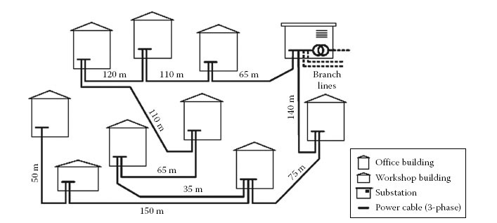
FIGURE 2.1
Topology of the low-voltage grid.
At first, a model for NB-PLC channels is given and a measurement methodology for obtaining the channel characteristics is described. In Sections 2.3 through 2.6, results of the evaluation of the essential channel properties, noise scenario, attenuation, signal-to-noise ratio (SNR) and access impedance are presented.
In order to describe the power line channel between a PLC transmitter (Tx) and a PLC receiver (Rx) within power line networks, we employ an expanded one-way linear time-varying model. As shown in Figure 2.2, it consists of mains access impedance, a linear filter and an additive noise source. t and f indicate the time and the frequency domains, respectively. It is used to describe the time-variant feature. The time-varying access impedance is the equivalent impedance seen into a power outlet. Together with the equivalent time-invariant output impedance of the transmitter, it determines the signal level that can be injected into the power line network. Let x(t) and sA(t) denote the original and the injected signals, respectively. X(t,f) and SA(t,f) are their spectral components, respectively. The signal level ratio of sA(t) to x(t) can be obtained by
(2.1) |

FIGURE 2.2
Equivalent electrical channel model.
HA(t,f) is usually frequency selective. The magnitude of HA(t,f) is usually smaller than 1 at most frequencies. This frequency-selective attenuation is caused by an impedance mis-matching and called coupling loss [1]. Many efforts have been made to compensate for the coupling loss. For example, adaptive algorithms and special coupling circuitry have been developed to match the impedance during the transmission [2]. The coupling loss can also be reduced by decreasing . For systems with these features, the influence of can be neglected. The received signal sR(t) is usually the attenuated and distorted counterpart of sA(t). For a linear system, the relation between sR(t) and sA(t) can be described by a TF H(t,f) in the frequency domain or by an impulse response h(t,τ) in the time domain. Generally speaking, h(t,τ) gives the response at time t caused by an impulse excitation applied at time t−τ.t and τ are also called the time of the observation instant and the time of excitation, respectively [3].sR(t) is related to sA(t) by
(2.2) |
h(t,τ) and H(t,f) fulfil the relation:
(2.3) |
The additive noise n(t) is a collection of interference seen at the receiver. With respect to the time variation, it is believed that the equivalent input impedance of many connected electrical appliances vary periodically and synchronous to mains frequency or to its harmonics. This phenomenon causes periodic frequency-selective fading both for transmit signals and interferences [4]. At the same time, many appliances themselves generate noise synchronously to the mains voltage [5,6].
From a signal processing point of view, the received signal r(t) is obtained by
(2.4) |
in the time domain or
(2.5) |
in the frequency domain. The channel TF H(t,f) describes the ratio (magnitude and phase) between the voltage level seen at the receiver and the voltage level injected into the grid (at a certain frequency and at a certain instant of time). In general, the channel TF is not symmetric for NB-PLC channels.
2.2 Measurement of Channel Parameters
The main emphases of this section are practical methods for the determination of noise, attenuation and impedance. Applicability for the variety of scenarios observed in reality is a key point for the selected approaches. Representative results will be presented and discussed.
Noise and access impedance have a cyclostationary behaviour and therefore the channel TF and the SNR are cyclostationary too. For this reason, the measurements applied were synchronised with the mains zero crossings. Due to the time variance of the channel, all parameters have to be determined simultaneously or at least within a short time. Multiple distributed measurement devices are involved in the procedure so that an overall picture of the whole grid can be obtained at one time. The following steps are performed periodically:
• Investigation of the idle channel: At the beginning of every cycle, the noise is recorded.
• Transmission/capturing of a test sequence: Every device (one after another) transmits a test sequence in a predefined order and synchronised with the mains. The sequence consists of sinusoidal signals at discrete frequencies.
The analysis of the captured data is done offline after the measurement. Every mains period is segmented into 20 intervals and statistics of selected parameters are calculated. Analysis of these statistics yields the short-time behaviour (within one measurement cycle) as well as the long-time behaviour of the channel.
In order to obtain all relevant parameters, a systematic measurement has to be carried out. Three highly flexible measurement and communication platforms [7] have been deployed for investigating low-voltage grids.
Each platform allows coupling arbitrary test signals into the power line as well as receiving and capturing signals. The received signal is streamed in realtime to a PC via USB interface. Therefore, signals of arbitrary length can be captured. For transmitting and receiving, a sample rate of 1.333 MSamples/s is used, which allows observations in the low-frequency range up to 500 kHz. The platform is synchronised with mains frequency. In addition, the device can also be configured as an orthogonal frequency-division multiplexing (OFDM) modem for data transmissions. The measurement campaign is divided into multiple measurement cycles. Totally, three steps are carried out during each cycle. In the first step, all three platforms record the local noise at the same time for 30 s. The second step measures the TFs from one location to another. The channel transfer characteristics feature usually no symmetry (see Section 2.4). Thus, each link has to be measured for both directions. As a result, there are totally six directions to investigate using three measurement platforms. One of the three platforms is allowed to transmit sounding signals while the other two must record the distorted signals for the estimation of channel distortions. In this way, always two directions are investigated at the same time. When one platform finishes the transmission, it switches into the receiving mode, and another platform starts to transmit sounding signals. This process continues until the attenuation values are captured for all six directions.

FIGURE 2.3
Measurement locations.
Several measurement campaigns have been carried out in a small low-voltage grid. The measurement results presented in this chapter are mainly based on two measurement campaigns: a 24 h measurement comprising three locations marked as S1, S2 and S3 in Figure 2.3 and another campaign also comprising three locations marked as S1, S3 and S4 in Figure 2.3. In addition, impedance measurements have also been taken in a suburban and a rural low-voltage grid for the investigation of the access impedance in Section 2.6.
Noise plays a significant role in the channel impairment. On the one hand, the transmit signal is largely attenuated; thus, the communication quality is mostly determined by the different noise scenarios seen at the receiver. On the other hand, the noise scenario deviates from the traditional AWGN model. It has more complicated spectral characteristics and features time-varying behaviours. It is necessary to analyse the noise in detail and deploy realistic noise scenarios to evaluate NB-PLC systems. This part describes the analysis of the noise scenario recorded during the measurement campaigns. At first an overview of the behaviour of the noise is given. This includes the short-time behaviour within one mains period as well as the long-time characteristics within hours or days. In the subsequent sections, a detailed analysis of the different kinds of noise is done. The typical noise scenario is divided into three classes: narrowband interferers, impulsive noise and coloured background noise. In addition, a new subclass in the narrowband noise class will be discussed. Interferers in this subclass have each a swept frequency. Due to this spectral feature, it is also named swept-frequency noise (SFN) in the following.
For the in-depth analysis, Nc mains cycles of the noise are captured and each mains cycle is segmented into 20 intervals (Figure 2.4), which leads to a time duration of about 1 ms (in a 50 Hz environment) and a length of L samples (about 1333 samples at 1.333 MSamples/s). Depending on the actual period length of the mains cycle, this value may vary slightly.
At first, the total noise power of each mains cycle segment is calculated (for each of the Nc mains cycles). For each of the intervals, the power spectral density is calculated by using the spectral estimator
(2.6) |
where
denotes the lth sample value within the ith interval and the nth mains cycle
wL is a Blackman–Harris window with a length equal to the length of one interval
Mean value and variance in both time and frequency domains for every mains cycle interval are evaluated.
Due to the varying impedance of the low-voltage grid at frequencies up to 500 kHz, not power but voltage amplitude has been examined and therefore the results are indicated in dBV2 or dBV2/Hz, respectively.
Figure 2.5a shows a result of the typical noise observed close to the consumer unit, that is, at the location of the electricity meter, of a building. Statistics of the total noise signal power within a mains cycle interval are shown in the upper part.
The signal energy calculated for intervals of 1 ms per mains cycle varies strongly within one mains cycle, but is periodic with 10 ms. Between different intervals within one mains cycle, deviations of >15 dB can be observed. The noise energy is mainly concentrated at the maximum and the minimum of the mains voltage.

FIGURE 2.4
Mains cycle segmentation.
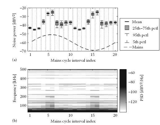
FIGURE 2.5
Received noise power over mains cycle interval. (a) Statistics of overall noise power and (b) noise power distribution over frequency (mean value).
In Figure 2.5b, the frequency spectrum of one mains cycle is shown. The noise power is concentrated to its largest extent on frequencies below 70 kHz. The noise bandwidth exceeds this frequency band at the same time intervals as the noise power per cycle part increases in the time domain. This is due to the mostly impulse-like characteristics of the time signal at these instants of time. Although the noise bandwidth is increased, however, most of the additional power introduced by impulses is still located below 70 kHz. Furthermore, narrowband noise components become apparent at various frequencies. The respective powers of these narrowband interferers vary only slightly over in-cycle time and in general strongly depend on the particular location of the measurement.
For the long-term analysis, we concatenate the courses of the median noise signal power over the mains cycle obtained from the short-term analyses.Figure 2.6 depicts the results for a 24 h measurement. The characteristic pattern of the noise power over the mains cycle remains almost unchanged over several hours. A clear distinction can be made between daytime and night-time. Noise power reduces significantly during night-time.
In summary of the overview of the noise scenario, the median noise signals are found to be approximately cyclostationary for relatively long periods of time. The course of the median noise power within a mains cycle shows characteristic patterns that remain constant for interval lengths in the order of hours. Depending on the instant of time within the mains cycle, the noise power distribution (noise power spectral density) over frequency varies in accordance with the noise power over time, since noise power maxima in the time domain coincide temporally with increased noise bandwidth.
In the following sections, a detailed analysis of the different noise classes is done.
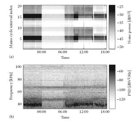
FIGURE 2.6
Noise power distribution over 24 h: (a) overall noise power within each mains cycle interval and (b) noise power distribution over frequency (up to 100 kHz).
This interference class is characterised by a significant noise level in the frequency domain compared to the background noise [1]. Disturbances at frequencies such as 25, 30, 49, 55, 75 and 82 kHz have been measured. They could be probably caused by switched power supplies. It has also been reported that the narrowband noise occurs mostly at frequencies below 140 kHz or above 410 kHz. The average bandwidth is about 3 kHz [8]. The narrowband interferers with time-invariant amplitude level have been well investigated. Modelling and emulating this kind of noise is also straightforward. Due to the time-varying nature of the power line network, the envelopes of a number of narrowband interferers also exhibit dynamics. The following parts introduce an approach for the estimation of the time-varying envelopes. Finally, a simplified model will be proposed for describing these envelopes.
2.3.2.1 Estimation of the Noise Powers
Figure 2.7a shows a segment of a noise acquired in a university laboratory. This segment lasts for 40 ms. The noise waveform in the time domain is dominated by impulsive disturbances. Furthermore, the overall envelope of the non-impulsive components changes with time. As shown in the spectrogram of the short-time Fourier transform (STFT) in plot (Figure 2.7b), there is a significant spectral component at around 64 kHz with a bandwidth of 4 kHz. The spectral density changes periodically. The local maxima are synchronised to the peak of the mains voltage. It is a good example of the narrowband interference with the cyclostationary features. In order to estimate the time dependence of its envelope, the influence of the other noise types such as the coloured background noise and the impulsive noise should be reduced as much as possible.

FIGURE 2.7
Narrowband noise with cyclostationary feature: (a) waveforms of noise and scaled mains in the time domain and (b) STFT spectrogram of noise (Blackman window, window length: 500 μs, overlap ratio: 83.33%). Both (a) and (b) share the same abscissa.
Figure 2.8 shows the STFT of the noise segment from another point of view.bM denotes the frequency band that contains the most significant noise power.bL and bR are the direct neighbouring bands to the left and right of bM, respectively. bL and bR have the same band-widths as bM. Gaps are inserted between bL and bM as well as between bM and bR so that the tails of each band will not interfere the other two bands.
The PSD of the background noise is relatively small compared to that of the narrowband noise. Therefore, for simplicity it is assumed that the background noise has the same noise power spectral density in all three bands. The spectra of short impulses usually exhibit wideband character. The PSD values are decreasing over frequency. Since these three bands are relatively short in comparison with the bandwidth of the impulsive noise, and they are close to each other, it is assumed that the power of the impulsive noise is a linear function of the frequency. Therefore, the power falling into bM is approximated by the mean value of the noise powers in bL and bR for this impulsive noise:
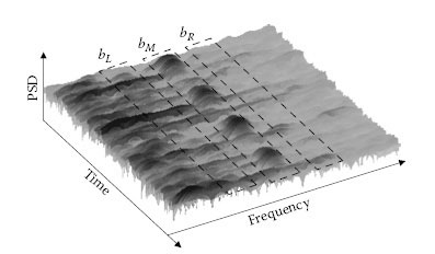
FIGURE 2.8
STFT of noise segment.bM is the middle frequency band.bL and bR are the left and right neighbouring bands, respectively.
(2.7) |
where and denote the power values of impulsive noise in logarithmic scale in bM, bL and bR, respectively. The linear-scale noise power in the middle band can be estimated using
(2.8) |
2.3.2.2 Reconstruction of Noise Waveforms
Figure 2.9 shows a flow chart for the steps to reconstruct the narrowband interferer nnbn(t) in the time domain. The basic idea is to estimate the envelope AM(t) and the oscillation waveform separately and then modulate using AM(t). Three FIR band-pass filters are used to obtain the waveform of the noise components located in each band.fM, fL and fR denote the middle frequencies of bM, bL and bR, respectively. Each filter is followed by a square operator and a low-pass filter with cut-off frequency fE. These two components are used to estimate the time-variant envelope of the total noise power falling in each frequency band.Ptotal(t), PL(t) and PR(t) denote the envelopes for the middle, the left and the right band, respectively. Figure 2.10a shows an example of the estimated envelopes for PL(t), Ptotal(t) and PR(t), respectively. The zones A1 to A5 cover the impulses that superimpose the narrowband interferer, while B1 and B2 cover the impulses appearing in the intervals between two narrowband interferers.nM(t) in Figure 2.10b is the filtered waveform corresponding to the narrowband interferer superimposed by impulsive and background noise.PL(t) and PR(t) are used to estimate the non-narrowband noise power PM(t) for the middle band.

FIGURE 2.9
Flow chart for detecting and extracting a single-frequency narrowband interferer.

FIGURE 2.10
(a) Estimating envelopes for all three sub-bands and (b) extracting the envelope of the narrowband interferer. Both (a) and (b) share the same abscissa.
In the next step, PM(t) is subtracted from Ptotal(t) and the difference ΔP(t) contains mainly the narrowband interferer. The error caused by the background noise can be further reduced by smoothing ΔP(t) properly. A comparator compares the smoothed ΔP(t) with a threshold xth. A value greater than xth indicates a valid envelope for the narrowband noise; otherwise, it is considered to be invalid and is forced to be zero. In this way, the power envelope of the narrowband interferer Pnbn(t) can be estimated. Its square root AM(t) is the expected envelope of nnbn(t).
The key aspect in the extraction of is to keep in phase with nM(t). The first idea is to estimate the phase of nM(t) and use it to synthesise a sinusoidal waveform. The phase estimation algorithm can be very simple if the frequency does not change over time; otherwise, a sophisticated frequency tracking strategy must be implemented. An alternative method is to estimate and compensate the fluctuation in the envelope of nM(t). The spectral feature is not affected in this way; therefore, it can also be applied even if nM(t) exhibits a time-varying frequency. This method is implemented by simply dividing nM(t) by Atotal(t), which denotes the square root of Ptotal(t).
In the last step, nnbn(t) is obtained by multiplying by AM(t). After having estimated the envelope and synthesised the narrowband interferer, nnbn(t) is removed from the original noise n(t) in the time domain.Figure 2.11 shows the remaining noise waveform in Figure 2.11a and the spectrogram of the STFT in Figure 2.11b. The investigated narrowband interferer disappears from the noise segment, while the background noise and the impulsive noise are not affected in comparison with those in Figure 2.7.
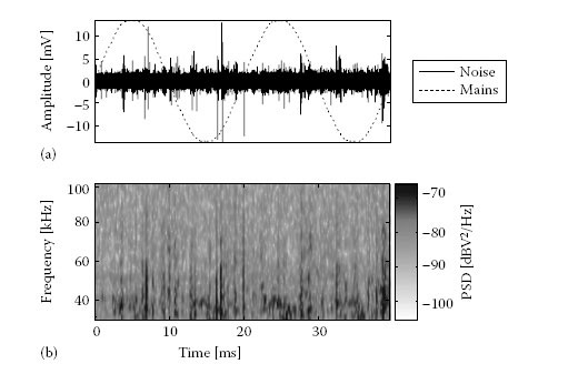
FIGURE 2.11
Waveform and STFT of residual noise; the cyclostationary narrowband disturbance has been removed. (a) Waveforms of modified noise and scaled mains in the time domain and (b) STFT of modified noise (Blackman window, window length: 500 μs, overlap ratio: 83.33%). Both (a) and (b) share the same abscissa.
2.3.2.3 Modelling Noise Envelope
The individual envelope can be modelled by one or more unsymmetrical triangular functions. The shape and the location of the normalised peak is determined by
(2.9) |
where t1, t2 and t3 are time points for the beginning, peak and end of the triangular curve, respectively.Figure 2.12 shows a normalised measured envelope and the reconstructed artificial envelope in plot (Figure 2.12a). The simulation is a sum of three fundamental shapes y1(t), y2(t) and y3(t).
In addition to the typical narrowband interferers, a subclass of interferers with time-varying frequencies has been observed in both indoor channel and the access domain. Due to the feature in the frequency domain, it is called SFN in the following parts.
2.3.3.1 Typical Waveform and STFT
Figures 2.13 through 2.15 show some measured SFNs. A measurement was made in a university laboratory where several PCs, fluorescent lamps, an uninterruptible power supply (UPS), a printer and several measurement devices form the appliance scenario. The noise waveform shown in Figure 2.13a is filtered by a band-pass FIR filter with a passband between 22 and 35 kHz. The scaled mains voltage is shown in the same plot to illustrate the synchronisation of the noise envelope with the mains frequency. Obviously, the noise envelope reaches the maximum at the same time as the mains voltage reaches the absolute peak value. The spectrogram of the STFT in Figure 2.13b shows two intersecting periodic traces. The first trace starts with 22 kHz at about 2 ms and increases to 32 kHz linearly within 5 ms. The second frequency trace decreases from 30 to 22 kHz in the same time interval.

FIGURE 2.12
Measured and simulated envelope of narrowband interferers.

FIGURE 2.13
Measured periodic noise with rising and falling swept frequencies at the same time: (a) waveform in time domain; the envelope fluctuates periodically and synchronised by mains voltage and (b) spectrogram of STFT applied to the waveform.
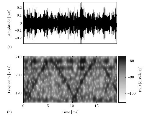
FIGURE 2.14
Measured periodic noise with sequential rising and falling swept frequencies: (a) waveform in time domain and (b) STFT.

FIGURE 2.15
Measured noise with rising and falling swept frequencies at substation: (a) waveform in time domain and (b) STFT.
Figure 2.14 gives another example obtained at a transformer substation. Again, two periodic frequency traces can be observed. Similar to those traces in Figure 2.13, the frequencies here also change linearly and periodically. Nevertheless, the frequencies sweep in a much higher range, between 185 and 210 kHz. There is no overlapped area, and these two traces appear one after the other. In addition, the noise level does not show a significant fluctuation over time.
Figure 2.15 shows a third example. The noise level is much higher than the first two examples. The waveform looks like a damped oscillation with duration of about 2 ms. The spectrogram of the STFT illustrates a more complicated pattern. Obviously, the frequency does not change linearly over time. Instead, two convex-shaped traces can be observed. The longer trace starts with 140 kHz and decreases to 45 kHz. At the same time, the PSD increases to its maximum at 45 kHz. In the second part, the frequency increases until it reaches 140 kHz again. The second trace seems to be the first harmonic.
This waveform appears as a single noise event in our measurement. However, similar patterns can also occur periodically with a period of 10 ms [9] has reported multiple periodic noise of this kind and has named them recurrent oscillations. An example is shown in Figure 2.16 for a quick comparison. The noise has been recorded in the direct vicinity of a fluorescent lamp after this lamp had been turned on. The filtered noise waveform reaches almost 2 V. The individual oscillations have quite similar envelope as the one shown in Figure 2.15a. The spectral patterns between 30 and 140 kHz in the spectrogram also match the convex shape shown in Figure 2.15b very well.
All examples have some points in common. In the frequency domain, their instantaneous frequencies have small bandwidths but change with time, either linearly as shown in Figures 2.13 and 2.14, or nonlinearly such as the pattern in Figures 2.15 and 2.16 The sweeping bandwidth can range from tens to hundreds of kHz. Furthermore, almost all NB frequency bands could be disturbed. In the time domain, their envelopes can be periodic and synchronous to the mains frequency, or relatively constant. They can even be aperiodic and appear as individual lobes with high noise levels.

FIGURE 2.16
Periodic damped oscillation reported in [9]: (a) periodic waveform in time domain and (b) spectrogram of STFT, the scale of the colour map is ignored and only the spectral patterns are shown for simplicity. Both plots share the same abscissa.
One main source of this noise class are active power factor correction (PFC) circuits in power supply units of many end-user appliances, such as fluorescent lamps and PCs.Figure 2.17 shows a simplified circuit of a switch mode power supply (SMPS) with an inserted active PFC module.
In an SMPS without the PFC circuit, the input capacitor C is placed directly behind the rectifier diodes D1 through D4. Current iM is drawn from mains to charge C. As shown in Figure 2.18, C will only be charged when the rectified voltage u1 exceeds the voltage uC across C. As a result, iM has large spikes during the charging of the capacitor and is zero otherwise. This kind of waveform contains large amount of harmonics. At the same time, the power factor – defined as the ratio of the real power to the apparent power – is very low. A low power factor burdens the power utilities because they have to deliver more power than necessary. Meanwhile, the harmonic distortions degrade the power quality and causes electromagnetic compatibility (EMC) problems.

FIGURE 2.17
Simplified circuit of PFC boost pre-regulator. (From Fairchild semiconductor, Power factor correction (PFC) basis, Application note 42047, Rev.0.9.0, August 19, 2004.)

FIGURE 2.18
Voltage and current waveforms in an SMPS without any PFC module [11]: (a) voltage waveforms and (b) current waveforms, iME is the expected current waveform for a unity power factor.
The active PFC module is used to keep the current in phase with the mains voltage and to minimise the input current distortion so that the power factor can be raised. As shown in Figure 2.17, the PFC circuit is actually a boost converter that is mainly composed of an inductor (L), a pulse-width modulation (PWM) and a power MOSFET as a switch (S). The boost converter will be able to provide a higher voltage u2 than the peak value of u1 at its output. Simultaneously, iL must be well controlled so that iM is proportional to uM at any given instant. Implementation details of the control unit can be found in [10,11].Figure 2.19 shows waveforms of iM, iL and the PWM signal uPWM when the PFC operates in continuous mode. Suppose the inductor L is uncharged initially. When the switch closes at t0, uPWM becomes logic high. The inductor current iL increases linearly:
(2.10) |
where uL is the voltage across L and can be approximated as a constant within tON:
(2.11) |
The switch opens (low level of uPWM within time window tOFF) as soon as iL(t) reaches iMAX(t) at t1 and the inductor starts to discharge:
(2.12) |

FIGURE 2.19
Waveforms of current and PWM control signals generated by PFC circuit in continuous mode of operation..
where uL is now the voltage difference between u1 and uC:
(2.13) |
Due to the feature of the boost converter, uC will be greater than u1; thus, uL is now a negative value. Therefore, iL maintains its direction and decreases linearly. As soon as iL drops to iMIN, the switch closes again. In this way, the current drawn from mains iM is kept within the area defined by iMAX and iMIN. Its average value iAVE follows um and therefore is in phase with the mains voltage. Depending on the value of iMIN(t), the PFC module can operate in either discontinuous or continuous modes. In the first mode, iMIN(t) is zero over the entire mains cycle.iL can reach zero, and the current waveform swings between 0 and iMAX. If iMIN(t) is greater than zero and is synchronised with iMAX(t), such as the one in Figure 2.19, iL can never reach zero during the switching cycle.
The HF components in iM can be converted to voltage by any connected impedance. Although many SMPS have EMI filters inserted between their rectifier bridges and the power plugs, these filters are usually less effective to reduce the differential-mode noise for the frequency range up to 150 kHz. Therefore, most noise spectral components can still appear in mains and can be coupled into NB-PLC systems.Figure 2.20a shows a band-pass filtered waveform of iM. The spectrogram of the STFT is shown in Figure 2.20b. Similarities can be observed in both the noise waveform and the spectral characteristics between the synthesised noise and the measured noise shown in Figures 2.15 and 2.16.
More and more active PFC modules are being applied to reduce the harmonics emitted by end-user devices and to comply with international standards such as IEC 61000-3-2. Furthermore, active PFC circuits are the most favourable solutions to limit harmonics for lighting equipment with HF-ballast [9]. Therefore, the influence of the SFN on the system performance of NB-PLC will become larger. It is important to improve the robustness of communication systems against the SFN. Meanwhile, it is necessary to add this noise class to the noise scenario and to emulate it as accurately as possible.

FIGURE 2.20
HF components of iM obtained by applying a band-pass filter. Passband: 20–150 kHz: (a) filtered waveform and (b) spectrogram of STFT..
Impulsive noise is usually grouped into three different classes: periodic impulsive noise asynchronous to the mains frequency mainly caused by switched power supplies, periodic impulsive noise synchronous to the mains frequency caused by switching of rectifier diodes of power supplies and asynchronous impulsive noise originated from transients caused by switching events. Setting aside the time behaviours such as inter-arrival time, individual impulses have some features in common. In the time domain, the impulses are peaks with short duration and high magnitude levels. Instead of random waveforms of the background noise, the most impulsive noise have deterministic appearance patterns, such sharp rising edges followed by damped oscillations, low-level oscillations terminated by sharp endings [12], impulse chains either equal or not equal spaced [13]. In the frequency domain, the impulsive noise can be distinguished from the background noise by raised wideband PSD. Most measured impulses exceed the background noise spectral density for at least 10–15 dB within most portions of the frequency range. These common features apply not only for broadband PLC but also for NB-PLC.Figure 2.21a shows a noise segment dominated by rich impulsive noise and the background noise. All the narrowband interferers have been removed using the method introduced in Section 2.3.2.1.Figure 2.21b shows its instantaneous power and Figure 2.21c is a detailed view of the part between 16 and 17.5 ms. The difference between the level of the background noise n1(t) and the nnbn(t) of the impulse n2(t) is very large.

FIGURE 2.21
Measured noise in time domain: (a) noise waveform n(t), (b) n2(t) and (c) detailed view of n(t), corresponding to (c) in plot (a).
2.3.5 Coloured Background Noise
The coloured background noise is a collection of low-level noise from all possible sources. Its average power level is dependent on the number and type of connected and active electrical devices. Therefore, it can also be considered to have cyclostationary characteristics [6,13]. In order to investigate the time variance, it is necessary to divide the noise waveform into multiple segments and to estimate the instantaneous PSD of each segment. For this purpose, STFT is performed on the remaining noise waveform from which the narrowband and the impulsive noise have been removed. In addition to the variance in the time domain, the coloured background noise is supposed to have a smooth spectrum, the power spectral density is a decreasing function of the frequency [1,8]. Therefore, the STFT result is smoothed in the time and the frequency domains, respectively.Figure 2.22a shows the overlapped PSDs of all noise segments. The averaged PSD can be approximated by the sum of two exponential functions:
(2.14) |
where f is the frequency in kHz.Table 2.1 shows a set of coefficients that fits the averaged PSD.
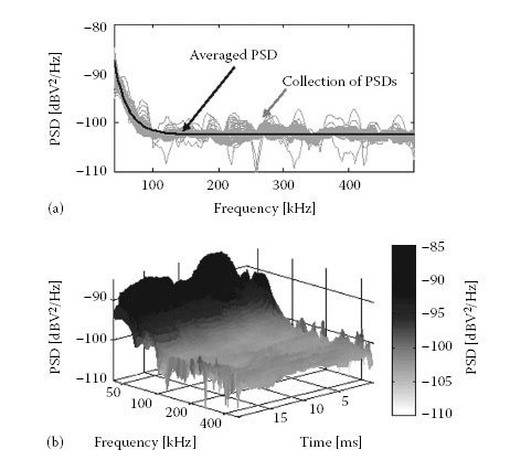
FIGURE 2.22
PSD of background noise. (a) PSD overlapped over time axis and (b) time–frequency view of PSD.
Coefficient of Polynomial
a |
b |
c |
d |
0.4413 |
–0.12 |
3.132 × 10⁻⁴ |
–1.32 × 10⁻⁴ |
Recommended Parameters
A0 |
A1 |
b |
c |
d |
200 |
1 |
–0.12 |
3 × 10⁻⁴ |
–3 × 10⁻⁴ |
Figure 2.22b shows the smoothed STFT of the remaining noise. The PSD fluctuation over time can clearly be recognised in the frequency range below 100 kHz. The maximum of the noise level is synchronous with the peak of the mains voltage. Perturbations can also be observed at higher frequencies. Since the noise level is comparatively low, these perturbations are ignored for simplicity.
Let m(t) denote the mains voltage, the parameter a(t) can be obtained by
(2.15) |
where A0 and A1 determine the scaling factor and the minimum level of the fluctuation, respectively. Table 2.2 lists a set of recommended parameters for modelling the time-variant. PSD of the background noise.
The channel attenuation is evaluated at discrete frequencies. For this purpose, a test sequence synchronised with the mains is transmitted. The sequence consists of sinusoidal signals at discrete frequencies fk at time index k consecutively by every device like illustrated in Figure 2.23a. The signals are captured by the receiver. By monitoring the injected test signal at the transmitter, any influence of the coupling circuits (assuming linear behaviour of the components) and the variation of the impedance at the transmitter can be compensated. The signal flow is depicted in Figure 2.23b.
With the Fourier transform of the transmitted signal S(f), the channel TF H(f) and of the noise N(f) assuming that
(2.16) |
the modulus of the channel TF at discrete frequencies fk can be estimated in the frequency domain by evaluating
(2.17) |

FIGURE 2.23
Evaluation of the attenuation: (a) test sequence flow and (b) signal path.
It is important to note that gives the ratio between the received voltage level and the transmitted voltage level for a certain frequency. Its attenuation is highly influenced by the particular appliances connected close to the particular receiver location. Therefore, the TF is not symmetric in general and has to be observed in both directions.
Mean value and variance for every mains cycle interval is calculated, as in the case of the noise scenario analysis.Figure 2.24 depicts exemplarily the resulting channel attenuation (up to 100 kHz) between two measurement locations over 24 h.
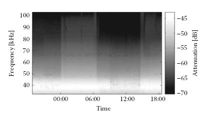
FIGURE 2.24
Variation of the attenuation over 24 h (S1 → S3).

FIGURE 2.25
Channel attenuation for downlink and uplink (S1 → S3).
Obviously, the TF varies over time, but the variation remains comparably small and the overall characteristics of the TF do not change during any of the observed intervals. Contrary to this, the differences between uplink and downlink can be significant. An example is shown in Figure 2.25.
The notch in the uplink is caused by narrowband interferers; due to low SNR, the signal attenuation cannot be calculated reliably for this frequency.
Having performed the analysis of the TF, the received signal level is known at each frequency. The next step is to obtain an estimate of the noise level. It is assumed that the behaviour of the noise energy at a certain frequency within a short period of time and within a small bandwidth is approximately constant. Thus, for time and frequency index k (see also Section 2.4), the Fourier transform of the noise estimate can be obtained by taking the mean value of the received noise in the pause prior to and after the test sequence and the energy at frequencies fk−4 and fk+4 while the signal fk is being transmitted:
(2.18) |
The modulus of the SNR can then easily be obtained by
(2.19) |
This estimation only holds true for assumption (Equation 2.16) in the evaluation of the TF. The proposed method is a pragmatic approach, since it is restricted to SNRs well above 0 dB. This is considered sufficient for our investigations because of the high energy of the transmitted test sequence. In fact, the energy of the test signal sequence is much higher than would be reasonable for any real implementation of a communication system.
Similar to the analysis of the noise scenario at first, the short-time behaviour within one mains cycle is investigated. The SNR for one frequency varies within one mains cycle. An example is shown in Figure 2.26. There is a clear variation within one mains cycle and an even stronger deviation relative to the median within the same mains cycle interval.
Considering the mean value of the SNR over one mains cycle and investigated for the whole time of 24 h and for all test frequencies basically reflects the results of the preceding analysis of noise scenario and TF and is depicted in Figure 2.27: the SNR remains constant for long periods of time.
In addition, Figure 2.28 displays statistics of the SNR at a receiver input. The overall SNR appears to be very high. However, these values should be put into perspective by the fact that the transmitter level is Umeas = 2.8 V and the observation window for each transmitted sinusoidal test signal is 20 ms. In other words, the SNR depicted would be valid for a single carrier system with a symbol rate of rmeas = 50 Bd. For simplification, we assume a Gaussian distribution for each frequency slot. A rough estimate of the actual SNR value for a communication system operating at a symbol rate of rcom and a transmit amplitude of Ucom can then be obtained from the measured SNR values by

FIGURE 2.26
Statistics of the SNR at 32.5 kHz within one mains cycle (s1 ↔ s4).

FIGURE 2.27
Variation of the SNR over 24 h (S1 ↔ S3).
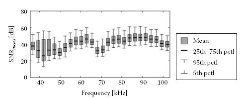
FIGURE 2.28
Statistics of the SNR for different frequencies (S1 ↔ S3).
(2.20) |
For a symbol rate of rcom = 10 kBd and a transmit amplitude of Ucom = 1 V, this leads to a reduction of the SNR of about 32 dB compared to the measurement results. In this case, the SNR between about 67 and 72 kHz given in Figure 2.28 would be reduced to about 0 dB. Obviously using a communication system utilising this frequency band would not make much sense in this environment.
For a multi-carrier system, the higher peak-to-average ratio of the transmit signal (compared to a single carrier system) in conjunction with a fixed maximum output amplitude of the transmitter can reduce this value additionally.
Exact knowledge of the impedance is a key aspect for power line modem development as well as for modelling channel transfer characteristics. Hence, this aspect is described explicitly.
The impedance seen at a particular point in a low-voltage grid is a superposition of any appliances online and its connecting lines. Although a lot of results regarding access impedance in the low-frequency range have been reported in the last few years – for example, [14,15,16] – updated measurements are needed due to the replacement of many appliances connected to the grid. Especially in the last years, more and more devices use SMPA.
Usually, a vector network analyser (VNA) is used for determination of scattering parameters. However, the expected impedance in the frequency ranging up to 500 kHz is very low and therefore there is a huge difference between the impedance measured and the internal impedance of the VNA, which is usually 50 Ω. In any case, a coupling circuit is needed to connect the VNA to the mains. This coupling circuit needs to be characterised in detail and its influence has to be compensated properly. Furthermore, the noise level in the live mains is high; therefore, for measuring very low impedance with an absolute value below 1 Ω, high power is needed to obtain accurate results. Hence, we choose direct measurement of current and voltage at the primary side of a coupling circuit for our measurements. Our test set-up for determination of the channel attenuation (see Section 2.4) can be used to evaluate the access impedance ZA simultaneously. This is illustrated in Figure 2.29. A shunt for measuring the current was inserted in the transmit path. The waveform generator includes a powerful front-end, which is able to deliver high currents to measure even very low impedance down to 0 Ω.A schematic of the set-up is depicted in Figure 2.29.

FIGURE 2.29
Impedance measurement set-up.
Every measurement is synchronised to the zero crossings of the mains cycle to allow an analysis of the cyclostationary behaviour of the power line channel.
To compensate for parasitic effects of the shunt resistor and the series impedance of the circuit, two measurements are done for the calibration: one with the output shorted (Um1/USh1) and one with a defined reference load of ZRef = 1 Ω (Um2/USh2):
(2.21) |
(2.22) |
The impedance of the shunt ZSh and the parasitic series impedance Zp can be estimated by
(2.23) |
(2.24) |
With Equations 2.21 through 2.24, the access impedance can be expressed as
(2.25) |
This is evaluated 20 times within each mains cycle to account for its variance. Measurements have been executed on different three-phase low-voltage distribution grids. The measurement equipment was connected as close as possible to the consumer unit. Three representative results are shown in Figure 2.30. In small buildings where all appliances are usually very close to the house connection box, the impedance is usually very low and irregular. Figure 2.30 shows a snapshot taken in a detached house. The dashed line is a snapshot taken at the same place but with a single additional energy-saving lamp (ESL) switched on. The example illustrates that the access impedance is mainly dominated by appliances with low input impedance and that are not very distant from the measurement location. This is caused by the fact that the modified access impedance can be seen as a parallel circuit of the input impedance of the appliance and the originally measured access impedance without the additional device. For low frequencies, the decoupling influence of the wires can be observed only for very long distances.

FIGURE 2.30
Access impedance measured at different premises (mean value).
At bigger buildings (block of flats and office building), the general behaviour is more regular. The resistance, as well as the (inductive) reactance, increases towards higher frequencies. The loads are farther away from the house connection point, which leads to an overall higher impedance. The absolute value of the impedance up to 100 kHz is usually below 10 Ω; towards lower frequencies, values below 1 Ω could be observed.
The impedance is stable over long periods of time, that is, in the order of hours. However, abrupt changes can occur by switching operations. The cyclic variation within one mains cycle (20 ms at 50 Hz) depends mainly on the nearby appliances. The variation for the three examples is depicted in Figure 2.31.
Contrary to the detached house, nearly no variation can be observed at the office building or the block of flats. This holds also true for a long-time observation of about 36 h, which is depicted in Figure 2.32. Despite the impedance drop at the beginning and at the end of the measurement – which was caused by switching on a fluorescent lamp very close to the measurement location – nearly no variation of the impedance can be observed at all.
The results obtained from different measurements have shown that for buildings with no appliances close to the house connection box, the impedance is inductive in general and increasing towards higher frequencies. For small buildings, where the length of the cables is shorter in general, the behaviour of the impedance is not predictable and depends mainly on the properties of the devices close to the consumer unit.
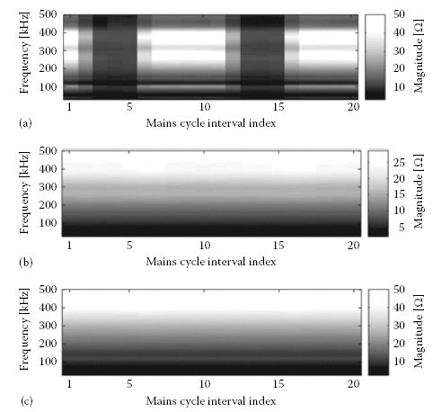
FIGURE 2.31
Variation of the access impedance within one mains cycle: (a) detached house (close to an ESL), (b) block of flats and (c) office building.

FIGURE 2.32
Long-time behaviour of the access impedance.
By means of the proposed measurement procedure, it is possible to investigate real-world power line channels comprehensively with respect to properties of the low-voltage mains grid relevant to communication systems. The suggested procedure allows for both short-term and long-term evaluation of different links of the grid at the same time. The measurement procedure has successfully been implemented and yielded valuable information on the channel properties in a small low-voltage network supplied by a single transformer substation. The noise signal power distribution over time and over frequency is periodic with the mains cycle period and its distribution patterns remain stable for periods of time mainly in the order of hours. Its overall characteristics depend strongly on location and on time of day in most cases.
Beside the well-investigated noise classes background and impulsive noise, a detailed look on the noise scenario identified two steady appearing noise classes: narrowband interferers with time-variant amplitude and switched frequency noise. Both have been investigated in detail and appropriate models have been proposed.
The influence of SFN on NB-PLC systems will be an important aspect in the near future due to the increasing number of SMPS in low-voltage grids. Our proposed model for SFN provides a good basis for comprehensive investigations.
The conclusions drawn from the measurement results presented earlier show that the channel TF is stable over long periods of time, but its overall characteristics depend on location. Its characteristics need not necessarily be symmetric. In conjunction with the noise observed at a receiver, this leads to a high variation of the SNR at the receiver, which is the crucial factor for reliable data transmission.
In general, reliable communication in the LF range is feasible for moderate data rates. However, a fixed communication set-up may fail due to the varying conditions. In fact, an adaptive communication approach is required for reliable NB-PLC systems.
Finally, a field study of an NB channel and noise emulator can be found in Chapter 21.
1. O. G. Hooijen, A channel model for the residential power circuit used as a digital communications medium, IEEE Trans. Electromagn. Compat., 40(4), November 1998, 331–336.
2. W. Choi and C. Park, A simple line coupler with adaptive impedance matching for power line communication, IEEE International Symposium Power Line Communications and its Applications, Pisa, Italy, 2007, pp. 187–191.
3. T. A. C. M. Claasen and W. F. G. Mecklenbraeuker, On stationary linear time-varying systems, IEEE Trans. Circuits Syst., 29(3), March 1982, 169–184.
4. M. H. L. Chan and R. W. Donaldson, Attenuation of communication signals on residential and commercial intrabuilding power-distribution circuits, IEEE Trans. Electromagn. Compat., EMC-28(4), November 1986, 220–230.
5. F. J. Cañete, J. A. Cortés, L. Dİez and J. T. Entrambasaguas, Analysis of the cyclic short-term variation of indoor power line channels, IEEE J. Sel. Areas Commun., 24(7), July 2006, 1327–1338.
6. M. Katayama, T. Yamazato and H. Okada, A mathematical model of noise in narrowband power line communication systems, IEEE J. Sel. Areas Commun., 24(7), July 2006, 1267–1276.
7. M. Sigle, M. Bauer, W. Liu and K. Dostert, Transmission channel properties of the low voltage grid for narrowband power line communication, in IEEE International Symposium Power Line Communication and Application, Udine, Italy, 2011, pp. 289–294.
8. J. Bausch, T. Kistner, M. Babic and K. Dostert, Characteristics of indoor power line channels in the frequency range 50–500 kHz, IEEE International Symposium on Power Line Communications and its Applications, Orlando, FL, March 2006, pp. 86–91.
9. A. Larsson, On high-frequency distortion in low-voltage power systems, Doctoral thesis, Universitetstryckeriet, Luleå, Sweden, 2011.
10. Fairchild semiconductor, Power factor correction (PFC) basics, Application note 42047, Rev. 0.9.0, August 19, 2004.
11. U. Tietze, C. Schenck and E. Gamm, Electronic Circuits: Handbook for Design and Application, 2nd edn, Spinger, New York, 2008.
12. M. Zimmermann and K. Dostert, Analysis and modeling of impulsive noise in broad-band powerline communications, IEEE Trans. Electromagn. Compat., 44(1), February 2002, 249–258.
13. J. A. Cortes, L. Diez, F. J. Canete and J. J. Sanchez-Martinez, Analysis of the indoor broadband power-line noise scenario, IEEE Trans. Electromagn. Compat., 52(4), November 2010, 849–858.
14. M. Arzberger, K. Dostert, T. Waldeck and M. Zimmermann, Fundamental properties of the low voltage power distribution grid, International Symposium on Power Line Communications (ISPLC), Proceedings, Essen, Germany, 1997.
15. O. G. Hooijen, A channel model for the low-voltage power-line channel: Measurement- and simulation results, Power Line Communications and Its Applications, Proceedings, Essen, Germany, 1997.
16. M. Katayama, S. Itou, T. Yamazato and A. Ogawa, A simple model of cyclostationary power-line noise for communication systems, International Symposium on Power Line Communications (ISPLC), Proceedings, Tokyo, Japan, 1998.