
Narrowband PLC Channel and Noise Emulation
CONTENTS
21.2 Emulating Narrowband Interferer
21.3 Emulating SFN Using Chirp Function
21.4 Emulating Time-Domain Waveform of Impulsive Noise
21.5 Emulating Time-Varying Background Noise
21.6 Emulation of Channel Transfer Function
21.6.1 Direct Convolution and FFT Convolution
21.6.3 Frequency Sampling Method
21.6.4 Extension of the Frequency Sampling Method
21.6.6 Realisation of Short-Term Time Variance
21.7 Emulator-Based Test Platform
21.8 Performance Evaluation of an OFDM System
21.8.2 Channel Transfer Function
21.8.3 Emulating Noise Scenario
With the advent and popularity of Smart Grids and advanced meter reading, more and more NB-PLC systems are available on the market. It becomes more difficult for customers to choose the best solution for their application. At the same time, system designers and researchers are developing a new generation of PLC modems. For system verification and benchmark testing, engineers are no longer satisfied with test methods and equipment adopted from other communication industries. For example, a vector signal generator is very popular in mobile phone and wireless tests. You can build a transmitter in it, generate the test signal to investigate the receiver and add noise and attenuation, so that the transmit signal seems to be distorted by a real channel. This method is accurate and flexible. However, it needs exact details of the device under test (DUT). If you want to test several devices of different technologies, you have to build a transmitter for each one. You can also connect the transmitter and receiver with a switchable attenuator; noise can be generated by using a low-cost function generator. Spectrum analysers and oscilloscopes can be used to measure signals and noise at the receiver. If the attenuation can work for both directions, a bidirectional communication can be tested. However, usually, the attenuator is flat for wide frequency range, so the performance against frequency-selective attenuation cannot be evaluated. It has low flexibility and also high cost. Alternatively, you can connect the DUT to mains network directly. Although such test results are highly realistic, they suffer from the lack of reproducibility and low flexibility.
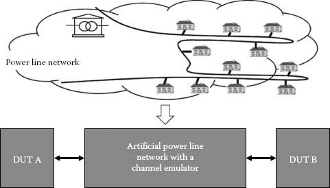
FIGURE 21.1
Test PLC systems using emulated channels.
Traditional equipment and approaches make the test of NB-PLC systems quite challenging. The new idea is to develop a hardware device, with which the sophisticated behaviours of real power line networks can be reproduced in a laboratory any time, as shown in Figure 21.1. Since it simulates the real-life power line channel in hardware, it can be called a channel emulator. The channel emulator indeed opens a new path to the flexible, reliable and technique-independent performance evolution of PLC modems.
An NB-PLC channel emulator has been developed according to the channel model mentioned in Chapter 2. As shown in Figure 21.2, the hardware design is composed of four modules: the input module emulates the access impedance with digitally switchable passive LCR networks. The analogue front end (AFE) contains a 12-bit analogue-to-digital converters (ADC) and two 14-bit digital-to-analogue converters (DACs). The sampling rates of the ADC and the DACs are configurable and set to 2 MS/s. Two additional digital-controlled attenuators are utilised to achieve a wide range of the signal-to-noise ratio (SNR) value with high accuracy. Each of the attenuators has a dynamic range of more than 75 dB with a resolution of 0.37 dB. The field-programmable gate array (FPGA) is the key component for the signal-processing part of the channel emulation. It implements digital filters and stores the impulse response values for multiple different channels. The frequency resolution of the reproduced transfer function can reach 2 kHz. The filter can be reloaded with a new set of coefficients within 10.5 μs during the filtering operation. The noise unit reproduces the noise scenario. The time variance control unit manages the switching among the access impedances, the updating of the digital filter and the modification of the noise parameters. The event table holds the time schedule of the switching events. The SNR unit determines the attenuation values for the signal and the noise paths. The output module scales the output to an appropriate voltage level. The emulator is connected to a computer via a standard serial interface, so that the emulation process can be controlled externally.

FIGURE 21.2
Block diagram of NB-PLC channel emulator.
21.2 Emulating Narrowband Interferer
The emulation of narrowband noise covers noise types with sinusoidal waveform. According to [1], this kind of noise has a bandwidth of several kHz. The amplitude level is greater than that of background noise. A narrowband noise model features three parameters: the centre frequency fm, the bandwidth Δf and the amplitude ANBN. The centre frequency refers to the fundamental oscillation of the noise. The centre frequency may change permanently, and its variation range is indicated by the bandwidth. The amplitude is a measure of the noise voltage level. The generation of a sinusoidal waveform is based on the phase accumulation method. As shown in Figure 21.3, this method utilises a phase accumulator and a look-up table. The phase accumulator consists of an adder and a phase register. The current phase P(n + 1) results from the modulo-N sum of the previous phase P(n) with the phase increment I:
(21.1) |
The look-up table is also called phase-to-amplitude converter. It contains one period of a sinusoidal waveform. The phase P(n) is fed to the look-up table as an address input, under which the amplitude value appears at the output. Multiplied with the factor ANBN, the amplitude values finally form the narrowband noise nbn with its fundamental oscillation.
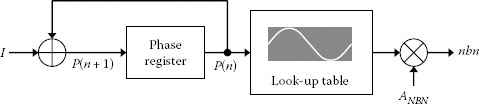
FIGURE 21.3
Phase accumulation unit.
The centre frequency fm depends on the clock frequency fa, on the number of stored amplitude values N as well as on the phase increment Im, that is,
(21.2) |
The variation of the centre frequency can be realised by incrementing or decrementing the phase increment I, that is,
(21.3) |
When I reaches its lower limit Imax−, it will be incremented by ΔI with each clock. When I reaches the upper limit Imax+, it is decremented by ΔI with each clock. The resulting instantaneous frequency f(I) is
(21.4) |
As a result, the bandwidth can be calculated by
(21.5) |
21.3 Emulating SFN Using Chirp Function
Due to the distinct spectral features of the SFN, it is reasonable to treat SFN in the frequency domain. The SFN can be modelled by a superposition of multiple chirp functions, such as
()
where
N is the number of fundamental chirp waveforms
mn(t) and fn(τ) are the envelope and the instantaneous frequency of the nth chirp, respectively
For the periodical noise with superimposed linear chirps and time-varying envelopes, the instantaneous frequency is obtained by
(21.7) |
where
f0 and f1 are the start and stop frequencies, respectively
Δτ is the duration within which the frequency changes from f0 to f1
mn(t) can be approximated by the scaled waveform of the mains voltage
The emulated noise together with coloured background noise is shown in Figure 21.4.
The chirp (see Chapter 2) has an instantaneous frequency which changes nonlinearly. By curve fitting the frequency trace, the instantaneous frequency can be approximated by
(21.8) |
where
τ0 is the time corresponding to the minimum frequency f0
f1 is the maximum frequency
The harmonic frequencies can also be modelled in Equation 21.8 conveniently. The envelope can be approximated by a Chebyshev window function whose Fourier transform side lobe magnitude is 120 dB below the main lobe magnitude. The synthesised noise waveform is shown in Figure 21.5.

FIGURE 21.4
Synthesised periodic noise with rising and falling swept frequencies. (a) Waveform in time domain and (b) shortterm Fourier transform (STFT).
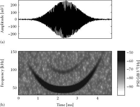
FIGURE 21.5
Synthesised periodic noise with nonlinearly swept frequencies. (a) Waveform in time domain and (b) STFT.
21.4 Emulating Time-Domain Waveform of Impulsive Noise
Since many impulsive noise types have similar magnitudes as the background noise, in the case where the time-domain noise waveform plays a less important role as the noise power spectral density (PSD), it can be assumed that the impulsive noise has a random waveform, and the appearance of such an impulse only raises the spectral level of the background noise shortly. This kind of impulsive noise can be generated by switching the background noise on and off according to a control pulse sequence. As shown in Figure 21.6, coloured background noise serves as noise source. The scaling unit determines the maximum amplitude of the noise. A switch is inserted between the noise source and the scaling unit. The switching sequence generator launches a sequence of ‘1’ or ‘0’. ‘1’ switches the noise source on to the scaling unit. The width of the pulse is determined by the duration of a ‘1’ level. If the ‘1’ level repeats within constant intervals, periodic impulsive noise is produced. Otherwise we get aperiodic impulsive noise. The former can be defined as synchronous with the mains frequency, if it repeats, for example, every 10 or 20 ms. All other rates correspond to periodic impulsive noise asynchronous with the mains frequency. The emulation of the time behaviour will be introduced later in the next section.

FIGURE 21.6
Generation of impulsive noise with stochastic waveform.
When an oscillation with exponential decay is expected, the impulsive waveform can be controlled by using three parameters: the pulse width, the maximal amplitude and the frequency of the oscillation. The noise can be modelled by modulating a sinusoidal waveform
(21.9) |
with an exponentially attenuated envelope
(21.10) |
where
ω0 = 2πf0 is the circular frequency of the sinusoidal signal
A0 is the initial amplitude
a0 is the time constant of the exponential decay
The modulated signal can be expressed as
(21.11) |
The implementation of the noise is shown in Figure 21.7. A segment of an exponential function with 1000 samples as well as a period of a sinusoidal signal with the same number of samples is created in MATLAB® first and stored as a look-up table within the FPGA hardware. The step width of the generated addresses can be configured with the parameters Δm and Δn. x1 and y1 are outputs of both look-up tables. They are multiplied with each other, and the product sequence forms the modulated exponentially decaying oscillation z.
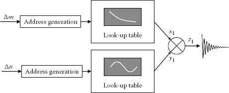
FIGURE 21.7
Emulation of impulsive noise with exponentially decayed waveform.
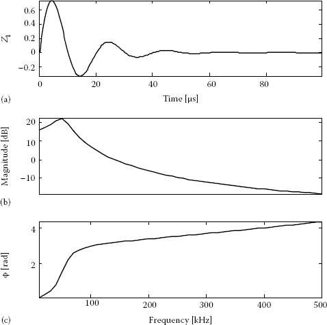
FIGURE 21.8
Emulated impulsive noise (a) waveform, (b) magnitude of the FFT and (c) phase vector of the FFT.
Combining both into the expressions of both signals, we get
(21.12) |
and
(21.13) |
where Ts is the period of the clock, with which samples are read out of the look-up tables. Changing the step widths of both addresses provides a variation of the sampling period. This can also be interpreted as an alteration of the time constant of the exponential decay and the frequency of the oscillation, respectively. In this way, both signals can be configured conveniently. An example of the emulated impulsive noise is shown in Figure 21.8.
21.5 Emulating Time-Varying Background Noise
Figure 21.9a shows the simulated PSDs; plot (b) shows the time–frequency representation of the simulated PSDs. It can be seen that the fundamental features of the time variance are reconstructed.

FIGURE 21.9
Emulated background noise. (a) PSD overlapped over time and (b) time–frequency representation of PSD.
21.6 Emulation of Channel Transfer Function
This part deals with the emulation of channel transfer function (CTF). From the signal processing’s point of view, the CTF influences the transmit signal in the form of a convolution of the transmit signal with the channel impulse response. To emulate the CTF means to implement the convolution algorithm. A starting point is the measured CTF in the form of magnitude, phase response and group delay denoted by and τ(i), respectively.
21.6.1 Direct Convolution and FFT Convolution
There are two possibilities to implement the convolution. One is the conventional convolution in the time domain using a digital filter. The other is the block convolution in the frequency domain. The first method obtains the channel impulse response samples and saves them as coefficients of the FIR filter. The transmit signal is correlated with the impulse response samples. The block convolution is based on the principle that a convolution in the time domain corresponds to a multiplication in the frequency domain. It converts the transmit signal in the frequency domain, multiplies the signal spectrum by the CTF and converts the products back in the time domain via IDFT. It takes advantages of the highly efficient fast Fourier transform (FFT), thus it is also called FFT convolution. By using the FFT algorithm to calculate the DFT, this kind of convolution can be faster than directly convolving the time-domain signals. Common methods to implement the FFT convolution are the overlap-add, the weighted overlap-add and the overlap-save methods. Details of these methods can be found in Ref. [2]. By comparing the number of major operations, it has been realised that the overlap-add method can be faster and more efficient than the FIR-based time-domain convolution if the filter order exceeds 20 or 40 for complex- and real-valued filters, respectively. Besides the implementation efficiency, the implementation must be able to reproduce time-varying convolution because typical NB-PLC channels exhibit time-varying responses. For this purpose, the FFT convolution could be quite simple and straightforward. Multiple CTFs can be stored in advance. A switch from one CTF to the other refers to a change of channel response. The switch rate depends on the length of each FFT block. In principle, the CTF shall not change during a FFT block. Therefore the time resolution can be as high as one FFT block for the emulation of time-varying CTF [3].
One disadvantage of the FFT convolution is an inherent delay within the signal-processing chain. To investigate this delay in detail, we use an overlap-add-based system as an example. Figure 21.10 illustrates a simplified block diagram. The system uses a NFFT point – FFT convolution to emulate the filtering effect of power line channels. The clock cycles that the FPGA spends in these modules and the corresponding redundancies are denoted by N1 through N4 and τ1 through τ4, respectively. The channel is supposed to have an impulse response of Nir points. It is padded with (NFFT – Nir) zeros, converted to frequency response H and stored in the system. The transmit signal is converted to digital samples by the ADC. The ‘overlap-add input’ module collects (NFFT – Nir) samples, adds Nir zeros to them to build a FFT block and delivers this block to the ‘FFT’ module. As a result, the first sample si(1) must wait for at least N1 sampling periods until it can be processed by the FFT module, and
(21.14) |
The ‘FFT’ module performs a NFFT point FFT on the block. The FPGA needs N2 clock cycles to finish the FFT. The frequency of this clock can be different from the signal sampling rate. The FFT results are delivered to the next module one by one. At the same time, they are multiplied by H. In this case, the multiplication lasts for at least NFFT clock cycles. The product vector is converted to waveform in the time domain by an IFFT of the same length as the FFT. The IFFT needs the same clock cycles as the FFT module. The ‘overlap-add output’ module adds the current IFFT block to the previous one with an appropriate superimposition. Finally, the output value corresponding to si(1) is obtained. The delays caused by each module are listed in Table 21.1.

FIGURE 21.10
Implementation of overlap-add method.
Delays Caused by Modules

The represented system uses 4096 point FFT and IFFT. The signal is sampled at 100 MS/s. The channel impulse response is supposed to be 15.36 μs; therefore, the length of the impulse response is 1536 samples. Each signal block contains 2560 samples, leading to a latency of 2560 sample periods in the input module. The FPGA needs 12,445 clock cycles for calculating FFT or IFFT [4]. Suppose the FFT, IFFT and the multiplications are performed at the maximum clock rate, for example, at 395 MHz for a Virtex 5, as a result, the latencies of the FFT and IFFT are both 31.51 μs, and the multiplication lasts for 10.37 μs. The minimum total latency reaches 99 μs, more than six times the channel impulse response. Applying the same conditions for convolution with a sample rate of 2 MS/s, the total latency is about 1.35 ms. Note that this large latency is not caused by the data transmission channel, but by the convolution algorithm itself. It may not impair the data transmission which deploys a preamble for the frame synchronisation, because both the preamble signal and the transmit signal are delayed identically. However, there are systems that use the zero crossings of the mains voltage for the purpose of bit and symbol synchronisation. Systems based on this kind of synchronisation are most S-FSK and other single-carrier systems as well as some orthogonal frequency division multiplexing (OFDM) systems [5]. The latency in the convolution can introduce an ‘artificial’ synchronisation error which degrades the data transmission in an unwanted manner. Therefore, it has serious consequences for the investigation of communication systems.
In contrast to the FFT convolution, the direct convolution does not have the inherent delay. The latency can be reduced by shifting the filter kernel properly. Nowadays, the development of silicon makes the implementation of complicated signal-processing algorithms possible for real-time applications. As a result of the comparison of both convolutions, we have selected direct convolution in the time domain for emulating the CTF.
Most efforts are made in the design of the filter kernel for direct convolution applications. The simplest and most straightforward way is the windowed frequency sampling method. The filter kernel can be obtained by performing an IFFT on the desired frequency response.
21.6.3 Frequency Sampling Method
The filter length is denoted by Nfir; therefore, the filter has an order of Nfir − 1. The frequency samples are expressed in linear scale
(21.15) |
The sampled values are given for the frequency of interest. The vector for the IFFT should be filled carefully so that the output of the IFFT is a real vector. For this purpose, the real and the imaginary parts should have an even and odd symmetry around the sample 0, respectively [6]. These symmetries are illustrated in Figure 21.11 where the zero-frequency bin is shifted to the centre. The real and imaginary parts are both normalised, and the plot has been blown up so that the significant values of both parts can be seen clearly.
The direct result of the IFFT cannot be used as a filter kernel. It may cause aliasing in the time domain during a convolution. The dashed curve in Figure 21.12 presents the IFFT result of the CTF that is shown in Figure 21.11. The IFFT result needs to be shifted and windowed to obtain a valid filter kernel [6]. Obviously, the direct IFFT has significant side lobes. The shifted IFFT does not go towards zero on both sides, leading to aliasing in the time domain, side lobes in the frequency domain and a loss of dynamic range of the filter response.
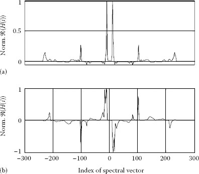
FIGURE 21.11
Frequency domain vector: (a) even symmetry for real part and (b) odd symmetry for imaginary part. The vector has 1000 samples, and the plot is enlarged, so that the frequency interval with significant energy, that is, between -240 and 240, is clearly visible.
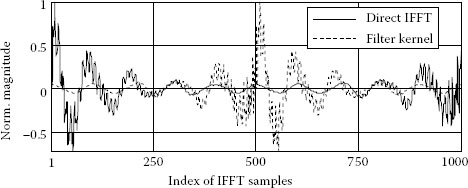
FIGURE 21.12
Direct output of IFFT and corresponding filter kernel.
To reduce the unwanted effects, the shifted IFFT vector can be multiplied by a window function. A window function has a bell-like waveform with its maximum in the middle, and both ends decline to zero. In this work, the Kaiser window function is used. The Kaiser window approximates the prolate-spheroidal wave functions in terms of the zero-order modified Bessel function. It tries to maximise the restricted energy in the frequency band of interest [7]. The Kaiser window is defined by
(21.16) |
I0(x) is the zero-order modified Bessel function of the first kind
(21.17) |
where α is the parameter which defines the width of the window. In the frequency domain, it determines the attenuation of the side lobes. Figure 21.13 shows the Kaiser window with α = 32 and the windowed filter kernel. The side lobes are reduced largely, while the most significant part between index 250 and 750 is well preserved.
The original filter kernel itself causes a delay of Nfir/2. The delay can be reduced by padding the right side with zeros and shifting the filter kernel to the left. The delay is constant for all frequencies. It is actually the latency of the FIR filter. Suppose this latency is denoted by tL. It must be considered in the filter design by adding it as a constant to the desired group delay. The delayed version of the desired complex CTF is obtained by
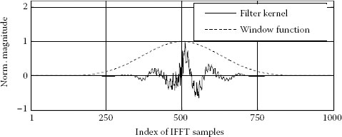
FIGURE 21.13
Kaiser window function with α = 32 and windowed filter kernel.
(21.18) |
where Nshift denotes the number of samples by which the sampled CTF vector should be shifted. Let fs be the sampling rate, Nshift can be obtained by
(21.19) |
The filter kernel should also be shifted to the left by Nshift samples in the time domain. And the resulting filter kernel is
(21.20) |
The operation (Equation 21.20) discards the part h(1) through h(Nshift) and leads to the loss of signal energy. If the shifting is driven too much to the left or to the right, a large part of the filter coefficients with significant energy may get lost. The deviation from the desired CTF becomes unacceptable. The phase error reaches 35° at 199 kHz. The maximum relative error of the group delay exceeds 18%. Another problem caused by windowing is the badly controlled error on either side of a discontinuity of the desired magnitude response. The frequency response between two adjacent samples is not constrained; therefore, the resulting frequency can deviate from the desired response between the samples. The obtained filter kernel is supposed to be suboptimal.
21.6.4 Extension of the Frequency Sampling Method
Sharp corners of the magnitude response can be smoothed by the aforementioned processing steps. Except that, most parts of the magnitude response can be preserved. It could be less critical for real PLC channels, because those sharp corners as shown in the first plot of Figure 21.14 are quite rare to see in the frequency range of interest. Therefore, this work focuses on reducing the error of the phase and the group delay responses. An iterative algorithm is presented to reduce the phase error below a defined boundary eb(f):
(21.21) |
The boundary is defined by
(21.22) |
where
e1 e2 and e3 are tunable parameters
is the desired magnitude response in linear scale
Obviously, the boundary is frequency dependent if e1 is a nonzero value. The phase errors at frequencies with high magnitude attenuation are less critical than those at other frequencies. Therefore, they are constrained with fewer efforts. In principle, the lower the magnitude attenuation, the lower the boundary of the phase error. The parameter e3 is constant over all sampled frequencies and determines the offset component of the phase error boundary. e2 adjusts the boundary difference between frequencies with high and low attenuation levels. A larger e2 leads to a larger boundary difference. e1 determines the ratio of the frequency-selective boundary component to the offset component. The steps listed in Table 21.2 are to be considered for the error reduction.

FIGURE 21.14
Deviation from desired CTF due to shifting, truncating and zero padding, as described by Equation 21.20. (a) Magnitude response, (b) error of phase response and threshold, (c) group delay and (d) relative error of group delay
Figure 21.15 shows an example of the result. The boundary is frequency dependent. The peak values of the boundary have good correlation to high magnitude attenuation. Compared with the plots shown in Figure 21.14, the phase and group delay errors are largely reduced at the cost of errors on sharp turns of the magnitude response. Large errors of phase and group delay occur at frequencies around 16, 84, 188, 230, 328, 404 and 490 kHz, at which the magnitude suffers from high attenuation and meanwhile features sharp corners. The group delays corresponding to moderate and low magnitude attenuation are even lower than 1%. The expected value of the relative error is as low as 1.71%. This coefficient set has a relatively large e2 in comparison with e3. The boundary differences at different frequencies dominate the boundary curve.
Steps to Reduce CTF Error
Step Index |
Operation |
1 |
Perform shift and truncate on the filter kernel using Equation 21.20 and obtain hshift1. |
2 |
Perform FFT on hshift1, obtain Hshift1 and calculate phase error Δ φ1. |
3 |
Multiply Hshift1 by exp(j ⋅ Δ φ1), perform IFFT and obtain hshift2. |
4 |
Repeat steps 1 and 2 once and calculate Hshift2, Δ φ2 and |
5 |
Multiply Hshift2 by , perform IFFT and obtain hshift3. |
6 |
Repeat steps 1 and 2 and calculate Hshift3 and Δ φ3. |
7 |
Check inequality of Equation 21.21, and find frequency bins fx at which the inequality is not fulfilled. |
8 |
Multiply Hshift3(fx) by exp[j ⋅ Δ φ3(fx)], perform IFFT and obtain hshift4. |
9 |
Repeat steps 6, 7 and 8 until the phase errors at all frequencies fulfil Equation 21.21 |

FIGURE 21.15
Improved results by applying iterative error reduction, e1 = 10−9, e2 = 1.9, e3 = 7.9 × 10⁻³, E{e(τ)} = 1.71%. (a) Magnitude response, (b) error of phase response and threshold, (c) group delay and (d) relative error of group delay.
The iterative extension to the frequency sampling method provides a flexible and straight-forward way to design FIR filters with custom frequency responses. In addition, the redundancy of the implemented filter can also be reduced to fulfil requirements in real-time applications. It is suitable for both short and long FIR filters with respect to the filter length. Nevertheless, unlike in conventional optimisation algorithms, the obtained filter coefficients using this method are still suboptimal. The user has to tune parameters e1 through e3 to obtain satisfied coefficients. The quality also depends on the specification of the error boundary. The iteration could have convergence problem if the boundary is not defined appropriately.
The emulated CTF is verified with a vector network analyser (VNA). Figure 21.16 compares the desired CTF (desired), the designed CTF (SIM), using the extended frequency sampling approach and the measured CTF (MEA) of the hardware implementation. For the magnitude response, the overall quality of the emulation is high. There are deviations of the measured magnitude from the design in the frequency range 400–500 kHz. This is caused by the antialiasing filter which has a 6 dB drop around 800 kHz. The measured group delay exhibits good agreement.
21.6.6 Realisation of Short-Term Time Variance
It has been mentioned that the channel response features both the long- and the shortterm variances. This part focuses on the emulation of the latter situation. Reference [3] models the time variance with eight fundamental states per mains cycle. To improve the time-frame resolution, a linear interpolation is performed on the fundamental states. As a result, more frequency responses are created – one for each frame – and the resolution reaches one response per time frame. With the help of the linear interpolation, the change of frequency response reaches a smooth transition. The FFT-based fast convolution provides a convenient way for the linear interpolation in the frequency domain. A new frequency response can be calculated by simply adding an increment to the previous one at each frequency. Consider the linear interpolation

FIGURE 21.16
Comparison of desired, simulated (SIM) and measured (MEA) CTF. (a) Magnitude response and (b) group delay.
(21.23) |
where n, m and k are indexes for the interpolated state, the fundamental states and the frequency bin, respectively. The increment ΔHm(k) is obtained by
(21.24) |
where Tm is the duration of the mth fundamental state. Obviously, ΔHm(k) remains constant within a fundamental state.
For the FIR filter-based direct convolution which is implemented in this work, it is desirable to realise the spectral interpolation with the help of operations in the time domain. In the time domain, the impulse response is obtained by
(21.25) |
Applying Equation 21.23 in Equation 21.25, a new impulse response can be expressed by the impulse response of the previous state and an increment
(21.26) |
where Δhm(i) is the inverse DFT of ΔHm(k). Since ΔHm(k) does not change within the mth state, Δhm(i) also remains unchanged. Figure 21.17 shows the frequency responses of six fundamental states, denoted by S1 through S6. These frequency responses are not from real-life measurements; instead, they are created artificially so that the state transitions can be observed clearly. S1, S2, S3 and S4 have band-pass characteristics. The attenuation level in S5 decreases linearly with frequency. S6 has a random frequency response. These fundamental states are interpolated linearly with 49 additional states between two consecutive fundamental states. Figure 21.18 shows the spectra of the fundamental and the interpolated states. The transmissions are smoothed and the boundaries are blurred.
The direct convolution delivers the output for each new input at the sampling rate. Theoretically, the resolution can be as high as the sample period if the new filter coefficients are also available within each sample period. Therefore, the resolution is only determined by the speed at which a complete coefficient set can be delivered to the FIR filter.
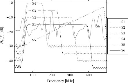
FIGURE 21.17
Frequency responses of the fundamental states S1 through S6.

FIGURE 21.18
Interpolated states of frequency response.
21.7 Emulator-Based Test Platform
Figure 21.19 shows an emulator-based test environment. It consists of a PC, a channel emulator, two coupling circuits (CCs), two line impedance stabilisation networks (LISNs) and an uninterruptible power supply (UPS). DUTs are connected to the platform by plugging the transmitter and the receiver in the reserved Tx/Rx sockets, respectively, corresponding to path P2 and P7. At the same time, interfaces of the DUTs for digital values are connected to the test server via P1 and P8. The PC is a test server. It generates diverse channels, configures the DUTs, controls the emulator and manages the whole test process. The UPS provides mains voltage as a power supply and a synchronisation source for zero-crossing detection-based DUTs. Meanwhile, it isolates the test environment from real mains networks. Each of the LISN provides well-defined stable impedance to the test environment and prevents the transmitted signal from reaching the receiver via the mains voltage path P9–P10–P11.
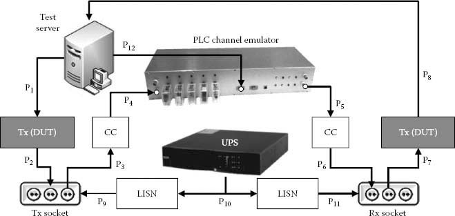
FIGURE 21.19
Channel emulator-based test platform.
High-frequency noise coming from the UPS can also be filtered by the LISNs. The CCs are necessary to separate the emulator from the high-voltage side and to exchange the ‘pure’ communication signals between the emulator and the DUTs. From the signal/data flow point of view, there is a closed loop: digital values, also called test patterns, are generated by the test server and transferred to the transmitter via P1. The analogue transmit signal is generated, and it reaches the emulator via P3 and P4.
21.8 Performance Evaluation of an OFDM System
Due to the capability of reproducing real-world channel characteristics, NB-PLC systems can be evaluated in laboratorial conditions using the proposed test platform. In order to investigate how well the laboratorial performance matches the system performance in the real channels, a case study has been performed. This case study consists of three steps. First of all, relevant channel characteristics such as the attenuation and noise scenarios are measured. Data transmissions are made using two OFDM-based PLC systems in each measurement pause. The bit error rate (BER) in each data transmission is recorded for an assessment of the link quality. Subsequently, the channel properties are characterised and reproduced using a PLC channel emulator. The same PLC systems are connected to the emulator. The same data transmissions are made, and the BER values are measured as well. Finally, the BER values obtained at the platform are compared with those BER values measured in the real PLC channels. The detailed procedure and the comparison result will be given in this part.
As mentioned in Chapter 2, the FPGA used for the measurement platform also hosts a flexible and easily adaptable OFDM modem core. Different multi-carrier systems can be configured conveniently. A simple OFDM realisation is configured on the FPGA for the case study. The system is using 48 carriers, ranging from 79 to 95 kHz. Each carrier is modulated with differential binary phase shift keying (DBPSK) for a robust data transmission. Each platform is equipped with a zero-crossing detector for mains voltage. The OFDM symbols are synchronised to the falling edges of the mains zero crossings. The total symbol duration – including a guard interval – is set to 1/6 of the mains period, that is, 3.3 ms in a 50 Hz environment. The frame length is nine OFDM symbols. 200 frames of random values are generated for each BER test. This corresponds to 86,400 bits binary data and results in accuracies of 1% and 3.4% for measuring BER values of 0.1 and 0.001, respectively [8].
21.8.2 Channel Transfer Function
It has been shown in Chapter 2 that the attenuation in NB-PLC channels exhibits small variation and weak time-varying feature. The difference between the highest and the lowest attenuation values is smaller than 10 dB. The variation of the attenuation at the same frequency does not exceed 6 dB, and it becomes even smaller towards higher frequencies. Therefore, the measured attenuation profiles are averaged first, and then only the averaged attenuation is emulated for each data link. Furthermore, the measured attenuation profiles are interpolated so that the frequency resolution of the measurement can be matched to that of the emulation. Figure 21.20 shows both the measured and the reproduced attenuation profiles. The asterisks correspond to the measured attenuation values, and the solid lines are the emulated CTFs. The reproduced channels have almost the same frequency-selective attenuation as their real-world counterparts. There is an error of 1.5 dB at around 30 kHz for the link from S1 to S3. However, its influence is neglectable since it is relatively small compared to the attenuation value (more than 50 dB) at this frequency, and it lies outside of the transmission band. The coupling loss is relatively small since the transmitter of our platform has very low output impedance. Therefore, its influence is neglected, and the access impedance is not emulated for this work.
21.8.3 Emulating Noise Scenario
For the noise emulation, we take the scenario measured at S2 as an example. Since the data transmission is made between 60 and 100 kHz, the noise is analysed and emulated for this frequency range. Due to the time-varying and frequency-selective nature, the analysis is performed in time and frequency domains using STFT. Figure 21.21 shows the waveform and the PSD in (a) and (b), respectively. Narrowband interferers with periodical fading can be observed at around 65.5, 67.5, 71, 76.5 and 88 kHz in (b). All the fadings seem to be synchronous with mains voltage and appear every 10 ms. A total of 12 narrow spectral peaks are found within 40 ms. They are the spectral components of broadband impulsive noises. By applying the analysis approach introduced in Chapter 2, these impulses can be divided into three groups. The group index and the arrival times of the individual impulses are shown in Table 21.3. It is obvious that the impulse in each group has a repetition rate of 100 Hz. Last but not least, the coloured background noise has weak time-varying feature in this frequency range. It can be modelled by a time-invariant exponential function of the frequency. By applying the emulation approaches for each noise type, the overall noise scenario is reproduced for S2. As shown in Figure 21.22, the emulated noise scenario retains the essential characteristics.

FIGURE 21.20
Comparison of measured and emulated transfer functions. The asterisks correspond to the measured attenuation values, and the solid lines are the emulated CTFs. Transfer functions for links (a) S2 → S3 and S1 → S3, (b) S3 → S1 and S2 → S1 and (c) S3 → S2 and S1 → S2.
Figure 21.23 illustrates the BER results measured during the channel measurement (‘MEA’ bars) and in the emulator-based test platform (‘EMU’ bars). The link from S3 to S2 has the best communication quality, while the two links between S1 and S2 as well as the link from S2 to S1 have very high BER values. The BER results obtained by using the test platform are very close to those of the field tests. Therefore, the laboratorial test platform can also be used to predict the system performance in the real-life channel. We can even produce worst-case channel conditions obtained from measurements and apply them to test different PLC systems. Systems that pass through these worst cases could have reliable and robust performance later in the real-life application. In this way, the complexity and period of selecting the best PLC solution can be largely reduced.
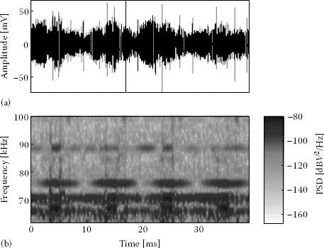
FIGURE 21.21
Measured noise scenario for S2. (a) Noise waveform in the time domain and (b) STFT of the noise waveform.
Arrival Time and Group Index
Group Index |
Arrival Time (ms) |
1 |
3.3, 13.3, 23.3, 33.3 |
2 |
5.5, 15.5, 25.5, 35.5 |
3 |
6.8, 16.8, 26.8, 36.8 |

FIGURE 21.22
Emulated noise scenario for S2. (a) Amplitude over time and (b) PSD over frequency and time.

FIGURE 21.23
Comparison of BER results.
This chapter has introduced a channel emulator for NB-PLC channels in LV mains networks. The channel emulation is based on a three-stage equivalent electrical model. A test bed has been built by using this emulator for the evaluation of data transmission on the physical (PHY) layer. Digital FIR filters are utilised to emulate the CTF. An extended frequency sampling algorithm provides a flexible and straightforward way to design such FIR filters for emulating any customised complex-valued CTF. In addition, recommendations are given to reduce the redundancy of the implemented filters, so that requirements for real-time applications can be met.
Narrowband interference features significant noise levels in the frequency domain in comparison with background noise. Envelopes of a number of narrowband interferers exhibit strong dynamic and time-varying features. A band-pass filtering-based approach is proposed for the estimation of the time-varying envelopes. This approach can detect broadband impulsive noise and eliminate its influences on the estimation. The typical sinusoidal waveform of narrowband interference can be generated by using the phase accumulation method. The estimated envelopes can be modelled by unsymmetrical triangular functions. In addition to the typical narrowband interferer, a class of interferers with time-varying frequencies, called swept-frequency noise in this thesis, has been observed both in indoor and access domain. Such interference is usually caused by active power factor correction (PFC) circuits in power supply units of many end-user appliances, such as fluorescent lamps and PCs. Emulation is possible by using chirp functions.
For impulsive noise, detection can be made by comparing the power of segmented noise waveforms with a constant threshold. In cases where the exact course of a noise waveform is unimportant, impulsive noise can be generated by switching the background noise on and off according to a control pulse sequence. Otherwise, it can be emulated as an exponentially attenuated oscillation. For coloured background noise, an accurate estimation can only be made after all the other noise classes have been removed. Its power level depends on the number and type of connected and active electrical devices. Coloured background noise also exhibits cyclo-stationary characteristics synchronous with the mains frequency, and its smoothed spectrum can be approximated by the sum of two exponential functions.
A case study made in a small low-voltage grid on a university campus has shown that the test results obtained by using the test platform are very close to those of the field tests. Therefore, the laboratorial test platform can also be used to predict the system performance in the real-life channel. The channel emulator indeed opens a new path to the flexible, reliable and technology-independent performance evaluation of PLC modems.
1. J. Bausch, T. Kistner, M. Babic and K. Dostert, Characteristics of indoor power line channels in the frequency range 50–500 kHz, in IEEE International Symposium on Power Line Communications and Its Applications, Orlando, FL, 2006, pp. 86–91.
2. L.R. Rabiner and B. Gold, Theory and Application of Digital Signal Processing, Prentice-Hall, Englewood Cliffs, NJ, 1975.
3. F.J. Cañete, L. Díez, J.A. Cortés, J.J. Sánchez-Martínez and L.M. Torres, Time-varying channel emulator for indoor power line communications, in IEEE Global Communications Conference, New Orleans, LA, 2008, pp. 2896–2900.
4. XILINX, LogiCORE IP fast Fourier transform v7.1, product specification, DS260, March 2011.
5. T. Kistner, M. Bauer, A. Hetzer and K. Dostert, Analysis of zero crossing synchronization for OFDM-based AMR systems, in Proceedings of the IEEE International Symposium on Power Line Communications and Its Applications, Jeju Island, Korea, April 2008, pp. 204–208.
6. S.W. Smith, The Scientist and Engineer’s Guide to Digital Signal Processing, 2nd edn., California Technical Publishing, San Diego, CA, 1999.
7. F.J. Harris, On the use of windows for harmonic analysis with the discrete Fourier transform, Proc. IEEE, 66(1), 51–83, January 1978.
8. M.G. Bulmer, Principles of Statistics, Dover Publications, Inc., New York, 1979.