
Chapter 5
Graphene Nanotechnology
Katsunori Wakabayashi
Department of Nanotechnology for Sustainable Energy, Kwansei Gakuin University, Gakuen 2-1, Sanda 669-1337, Hyogo, Japan
5.1 Introduction
Graphene, a single-layer hexagonal lattice of carbon atoms, is a fascinating system for fundamental studies in condensed matter physics, as well as a promising candidate material for future applications in carbon-based nanoelectronics and molecular devices [1–4]. Since the honeycomb crystal structure of graphene consists of two nonequivalent sublattices, graphene has a unique band structure for the itinerant ![]() -electrons near the Fermi energy. In particular, the motion of electrons in graphene near the Fermi energy is well described by the massless Dirac equation (Weyl equation). Since electrons in graphene have Dirac electron nature, graphene provides an environment for highly unconventional two-dimensional (2D) electronic properties [5–7] such as the half-integer quantum Hall effect [2, 3], the absence of backward scattering [6, 8, 9], Klein tunneling [10]. Owing to its high electronic mobility [11] and thermal conductivity [12], graphene is recognized as one of the key materials for realizing next-generation electronic devices.
-electrons near the Fermi energy. In particular, the motion of electrons in graphene near the Fermi energy is well described by the massless Dirac equation (Weyl equation). Since electrons in graphene have Dirac electron nature, graphene provides an environment for highly unconventional two-dimensional (2D) electronic properties [5–7] such as the half-integer quantum Hall effect [2, 3], the absence of backward scattering [6, 8, 9], Klein tunneling [10]. Owing to its high electronic mobility [11] and thermal conductivity [12], graphene is recognized as one of the key materials for realizing next-generation electronic devices.
In nanometer-sized graphene-based electronic devices, the effect of edges on the electronic properties of graphene becomes crucial. The presence of edges in graphene has strong implications for the low-energy spectrum of the ![]() -electrons [13–15]. There are two basic edge shapes, armchair and zigzag, which determine the properties of graphene ribbons. It has been shown that nanoribbons with zigzag edges (zigzag nanoribbons) possess localized edge states with energies close to the Fermi level [13–17]. In contrast, edge states are absent for ribbons with armchair edges.
-electrons [13–15]. There are two basic edge shapes, armchair and zigzag, which determine the properties of graphene ribbons. It has been shown that nanoribbons with zigzag edges (zigzag nanoribbons) possess localized edge states with energies close to the Fermi level [13–17]. In contrast, edge states are absent for ribbons with armchair edges.
The presence of graphene edge states results in a relatively large contribution to the density of states (DOS) near the Fermi energy in a nanoscale graphene system. Thus, these edge states induce the ferrimagnetic spin polarization along the zigzag edge [13, 16]. The properties of such magnetic states has been widely studied theoretically [13, 16, 18–23]. Since the structural or chemical modification of graphene edges affects the electronic states near the Fermi energy [23–27], they can be used to design the functionality of nanocarbon systems.
Several routes have been reported for the synthesis of graphene nanoribbons: a top-down approach using lithographic patterning of graphene samples [28, 29], solution dispersion and sonication [30], longitudinal unzipping of carbon nanotubes [31, 32]. In addition, recent bottom-up synthesis approach provides graphene nanoribbons with the atomically precise edge structures on metal surface [33–35]. Transport measurements were also demonstrated by several groups [28, 36–42].
In this chapter, we briefly review the theoretical aspects of nanoscale edge effects on electronic and magnetic properties of graphene system and discuss the possible application for the nanoscale devices.
5.2 Electronic States of Graphene
Electronic states of graphene near the Fermi energy are governed by ![]() -electrons which originate from
-electrons which originate from ![]() orbital of carbon atoms. Here we shall briefly review the
orbital of carbon atoms. Here we shall briefly review the ![]() -band structure of a graphene sheet [43]. Figure 5.1a and b show the lattice structure and the first Brillouin zone (BZ) of graphene, respectively. Graphene has a honeycomb lattice structure, and thus its first BZ is hexagonal. The corners of the first BZ are called
-band structure of a graphene sheet [43]. Figure 5.1a and b show the lattice structure and the first Brillouin zone (BZ) of graphene, respectively. Graphene has a honeycomb lattice structure, and thus its first BZ is hexagonal. The corners of the first BZ are called ![]() or
or ![]() points, which are also referred to as Dirac points because the energy spectrum at these corners can be described by the massless Dirac equation (Weyl equation). A single-orbital nearest-neighbor tight-binding model for the
points, which are also referred to as Dirac points because the energy spectrum at these corners can be described by the massless Dirac equation (Weyl equation). A single-orbital nearest-neighbor tight-binding model for the ![]() -electron network gives energy dispersion of graphene in momentum space as
-electron network gives energy dispersion of graphene in momentum space as ![]() , namely,
, namely,
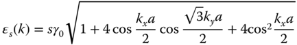
with ![]() 1.
1. ![]() is the transfer integral between nearest-neighbor carbon sites, which has been estimated to be about 2.75 eV in a graphene system [5]. Because one carbon site has one
is the transfer integral between nearest-neighbor carbon sites, which has been estimated to be about 2.75 eV in a graphene system [5]. Because one carbon site has one ![]() -electron on average, only the
-electron on average, only the ![]() band is completely occupied. Thus,
band is completely occupied. Thus, ![]() and
and ![]() correspond to the conduction and valence bands, respectively. Figure 5.1c depicts the energy band structures of graphene with the corresponding DOS. Thus, the Fermi energy is at
correspond to the conduction and valence bands, respectively. Figure 5.1c depicts the energy band structures of graphene with the corresponding DOS. Thus, the Fermi energy is at ![]() , and
, and ![]() and
and ![]() become Fermi points. Figure 5.1d is the 3D plot of energy band structure in 1st BZ.
become Fermi points. Figure 5.1d is the 3D plot of energy band structure in 1st BZ.
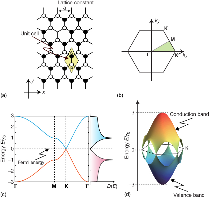
Figure 5.1 (a) Graphene sheet in real space, where the black (white) circles denote A(B)-sublattice sites;  is the lattice constant and
  and
and  are the primitive vectors. (b) First BZ of graphene.
  ,
,  ,
,  . Note that there are three
  and
and  points, which can be connected by the reciprocal lattice vectors. (c) Energy band structure of graphene within the irreducible BZ with the DOS. (d) 3D plot of energy band structure.
5.3 Graphene Nanoribbons and Edge States
The presence of a graphene edge has a strong impact on the electronic states of Dirac electrons. There are two types of graphene edge: armchair and zigzag edges. These two edges have a 30![]() difference in their orientation within the graphene sheet. A large difference in the
difference in their orientation within the graphene sheet. A large difference in the ![]() -electronic structures is induced by the two types of graphene edges [13]. In particular, a zigzag edge exhibits localized states, whereas an armchair edge does not exhibit such localized states. The appearance of graphene edge states is a source of the peculiar magnetic and transport properties of nanoscale graphene, as will be discussed in the following section.
-electronic structures is induced by the two types of graphene edges [13]. In particular, a zigzag edge exhibits localized states, whereas an armchair edge does not exhibit such localized states. The appearance of graphene edge states is a source of the peculiar magnetic and transport properties of nanoscale graphene, as will be discussed in the following section.
The graphene nanoribbon model is useful for analyzing the electronic states of nanographene. Because of the periodicity along the longitudinal direction of nanoribbons, we can define the crystal momentum (wave number ![]() ) so as to apply the ordinal approach of solid state physics to these systems. The lattice structures of graphene nanoribbons are shown in Figure 5.2a and b. Figure 5.2a shows a graphene nanoribbon with armchair edges (armchair nanoribbon). Figure 5.2b shows a graphene nanoribbon with zigzag edges (zigzag nanoribbon).
) so as to apply the ordinal approach of solid state physics to these systems. The lattice structures of graphene nanoribbons are shown in Figure 5.2a and b. Figure 5.2a shows a graphene nanoribbon with armchair edges (armchair nanoribbon). Figure 5.2b shows a graphene nanoribbon with zigzag edges (zigzag nanoribbon).
We define the width of a graphene ribbon as ![]() , where
, where ![]() is the number of dimer (two carbon sites) lines for an armchair nanoribbon and the number of zigzag lines for an zigzag nanoribbon. Here all dangling bonds at graphene edges are terminated by hydrogen atoms.
is the number of dimer (two carbon sites) lines for an armchair nanoribbon and the number of zigzag lines for an zigzag nanoribbon. Here all dangling bonds at graphene edges are terminated by hydrogen atoms.
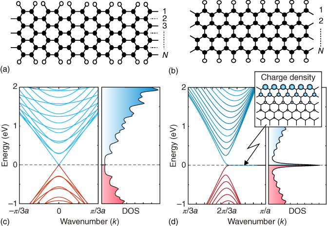
Figure 5.2 Structure of (a) armchair nanoribbon and (b) zigzag nanoribbon.  defines the ribbon width. (c) Energy band structure
  and DOS
  of armchair nanoribbons with
  (
( nm) and (d) zigzag nanoribbons with
  (
( nm). The inset shows the charge density distribution in real space at Fermi energy.
Note that the same number ![]() for both zigzag and armchair ribbons does not give the same ribbon width when the ribbons are measured by the same unit of length. Therefore, when we compare the physical quantities of zigzag and armchair ribbons with the same width
for both zigzag and armchair ribbons does not give the same ribbon width when the ribbons are measured by the same unit of length. Therefore, when we compare the physical quantities of zigzag and armchair ribbons with the same width ![]() , we will use the following definition
, we will use the following definition
where ![]() = (0.246 nm) is the lattice constant of graphene.
= (0.246 nm) is the lattice constant of graphene.
Figure 5.2c shows the DOS and energy band structures of armchair ribbons with width ![]() (
(![]() nm). The top of the valence band and the bottom of the conduction band are located at
nm). The top of the valence band and the bottom of the conduction band are located at ![]() . It is known that armchair nanoribbons become metallic when
. It is known that armchair nanoribbons become metallic when ![]() , where
, where ![]() . For semiconducting ribbons, the direct band gap decreases with increasing ribbon width and approaches zero in the limit of very large
. For semiconducting ribbons, the direct band gap decreases with increasing ribbon width and approaches zero in the limit of very large ![]() . For narrow undoped metallic armchair nanoribbons, an energy gap can be formed by Peierls instabilities at low temperatures [22, 44–46].
. For narrow undoped metallic armchair nanoribbons, an energy gap can be formed by Peierls instabilities at low temperatures [22, 44–46].
For zigzag ribbons, however, a remarkable feature arises in the band structure, as shown in Figure 5.2d. The top of the valence band and the bottom of the conduction band are always degenerate at ![]() , and the degeneracy of the center bands at
, and the degeneracy of the center bands at ![]() does not originate from the intrinsic band structure of the graphene sheet. These two special center bands flatten with increasing ribbon width. A pair of partial flat bands appears within the region
does not originate from the intrinsic band structure of the graphene sheet. These two special center bands flatten with increasing ribbon width. A pair of partial flat bands appears within the region ![]() , and makes the sharp peak in the DOS at the Fermi energy especially when the ribbon width is nanometer scale. The electronic states in the partial flat bands of the zigzag ribbons can be understood as localized states near the zigzag edge (edge states) as shown in the inset of Figure 5.2d [13–15, 47–49].
, and makes the sharp peak in the DOS at the Fermi energy especially when the ribbon width is nanometer scale. The electronic states in the partial flat bands of the zigzag ribbons can be understood as localized states near the zigzag edge (edge states) as shown in the inset of Figure 5.2d [13–15, 47–49].
The edge states are reasonably robust even if the graphene edge does not have a clear zigzag edge. Actually, a general edge structure that is not parallel to the armchair edge can have a zero-energy edge state, which was shown by analogy to the condition of the zero-energy Andreev bound state in an unconventional superconductor [50]. In addition, the analytical form of full energy spectrum and corresponding wave functions for the nearest-neighbor tight-binding model can be found in [51]. Even for an armchair edge, a localized state and a completely flat band can be obtained in the case of a strong imbalance of the on-site potential energy between two sublattice sites [25].
5.4 Spintronic Properties of Graphene
The presence of a sharp peak in the DOS near the Fermi energy should induce lattice distortion via the electron–phonon interaction and/or magnetic polarization via the electron–electron interaction. Because of the non-bonding character of the edge states, lattice distortion in the vicinity of zigzag edges is unlikely with the expected strength of the electron–phonon coupling [44]. The absence of lattice distortion was also confirmed based on the density functional theory (DFT) [22, 46].

Figure 5.3 (a) Schematic magnetic structure of a zigzag ribbon with  at
at  . (b) Energy band structure and corresponding DOS for same parameter set.
Figure 5.3a shows a schematic picture of the spin structure in real space for ![]() , which was evaluated by the mean field approximation of Hubbard model [13]. Here
, which was evaluated by the mean field approximation of Hubbard model [13]. Here ![]() is the strength of onsite Coulomb interaction between electrons. Although the vanishing total spin for the ground state is consistent with the exact statement of the half-filled Hubbard model [52], it can be seen that the magnetic moments align along a zigzag edge with a ferrimagnetic correlation. Figure 5.3b shows the energy band structure and corresponding DOS for
is the strength of onsite Coulomb interaction between electrons. Although the vanishing total spin for the ground state is consistent with the exact statement of the half-filled Hubbard model [52], it can be seen that the magnetic moments align along a zigzag edge with a ferrimagnetic correlation. Figure 5.3b shows the energy band structure and corresponding DOS for ![]() with
with ![]() . Since a finite
. Since a finite ![]() opens the band gap at
opens the band gap at ![]() accompanying with the spin polarization, the peak in the DOS at
accompanying with the spin polarization, the peak in the DOS at ![]() splits into two peaks. Recent experiment has reported the peak splitting of edge states for chiral graphene nanoribbons at low temperatures using scanning tunneling spectroscopy, which might be attributed to the occurrence of edge spin polarization [53, 54].
splits into two peaks. Recent experiment has reported the peak splitting of edge states for chiral graphene nanoribbons at low temperatures using scanning tunneling spectroscopy, which might be attributed to the occurrence of edge spin polarization [53, 54].
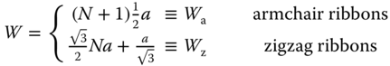
Edge spin magnetism along the zigzag edge is interesting from the viewpoint of the magnetic properties of nanographenes. In further, this magnetic states are very sensitive to the carrier doping [55]. Figure 5.4 shows the spin–spin correlation function for a zigzag graphene nanoribbon with a finite length, which is calculated by using the configuration interacation (CI) method. Here ![]() is the number of holes doped in the nanoribbon. Figure 5.4a is the spin–spin correlation function along a zigzag edge, which indicates the spin–spin correlation between a spin located 0th site of the upper (bottom) edge, that is, central site of a edge, and a spin located at
is the number of holes doped in the nanoribbon. Figure 5.4a is the spin–spin correlation function along a zigzag edge, which indicates the spin–spin correlation between a spin located 0th site of the upper (bottom) edge, that is, central site of a edge, and a spin located at ![]() th site. Since spins have ferrimagnetic correlations along a zigzag edge, they have the positive values. In zigzag nanoribbons, spin–spin correlation function does not have exponential decay, but power-low decay. This means that edge magnetism along a zigzag edge is rather robust and even after hole doping. On the other, Figure 5.4b is the spin–spin correlation function between upper and bottom edges. Negative values indicate that edge spins are antiferromagnetically coupled between upper and bottom edges. Interestingly, this antiferromagnetic correlation is rapidly decreased by the hole doping. In fact, the spin excitation energy becomes almost zero by hole doping, that is, magnetic ground state are expected.
th site. Since spins have ferrimagnetic correlations along a zigzag edge, they have the positive values. In zigzag nanoribbons, spin–spin correlation function does not have exponential decay, but power-low decay. This means that edge magnetism along a zigzag edge is rather robust and even after hole doping. On the other, Figure 5.4b is the spin–spin correlation function between upper and bottom edges. Negative values indicate that edge spins are antiferromagnetically coupled between upper and bottom edges. Interestingly, this antiferromagnetic correlation is rapidly decreased by the hole doping. In fact, the spin excitation energy becomes almost zero by hole doping, that is, magnetic ground state are expected.
Figure 5.4 Hole doping effect on edge magnetism of graphene nanoribbon. Spin–spin correlation function for a zigzag graphene nanoribbon with a finite length (a) along the zigzag edge and (b) between upper and lower edges.  is the number of holes. Here,
  .
.

Figure 5.5 Energy band structure and corresponding DOS for (a) zigzag graphene nanoribbon with all the edge carbon atoms replaced by boron atoms for  = 8. The solid lines and dashed lines denote the up- and down-spin states. (b) Their spin density profiles. The calculation was performed by the first-principles calculation.
The magnetic and transport states of zigzag nanoribbons can be chemically modified by replacing all the edge carbon atoms by boron atoms. As shown in Figure 5.5a, the linear energy bands appear near the Fermi energy resulting in the appearance of the mobile electrons, that is, metallic behavior. However, as each boron atom has one less electron compared to the carbon atom, the system becomes hole doped and the ground state shows ferromagnetic behavior with parallel alignment of spins along the same edge as well as within opposite edges, as can be seen in Figure 5.5b. There have been several other interesting reports about the possible ways to achieve the half-metallic or ferromagnetic behavior in graphene systems.
5.4.1 Electric Field Induced Half-Metallicity
The application of a transverse electric field to a zigzag nanoribbon can lift the spin degeneracy and induce a half-metallic state [56]. Half-metallic materials are crucial for the application of spintronics devices because they can be used as the source of spin-polarized current or as a spin-filtering device. A schematic figure of the DOS for half-metallic materials is drawn in Figure 5.6a. In half-metallic materials, the spin degeneracy near the Fermi energy is lifted, and one of the two spin states becomes absent. Thus, only one spin component contributes to the electronic conduction as a spin-polarized current.
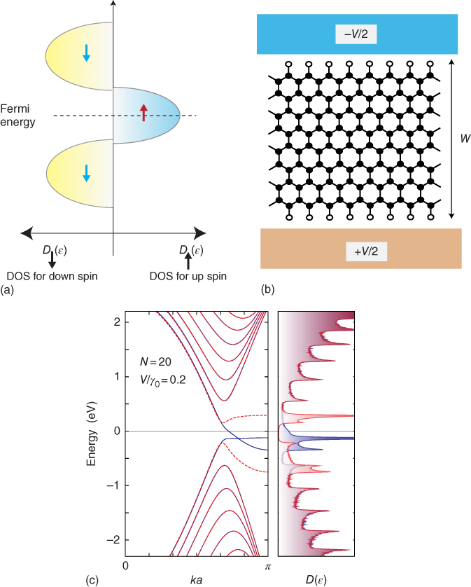
Figure 5.6 (a) Schematic figure of DOS for half-metallic materials. The left (right) side shows the DOS for  - (
- ( -) spins. The degeneracy between two spins is lifted. Since only one of the two spin states has a finite DOS near the Fermi energy, only up spin states (in this case) contributes to electronic conduction. Thus, half-metallic materials can be a source of spin-polarized current or spin-filtering materials because the other spin states (in this case, down-spin) do not allow conduction. (b) Schematic figure of zigzag nanoribbons with the application of a transverse electric field. (c) Energy band structures and corresponding DOS for zigzag nanoribbons with
  . Here the hopping between next nearest neighbor sites is included. The applied electric field is
  . The solid lines and dashed lines in (c) denote down- and up-spin states. Here the calculation was performed by the mean field Hubbard model with the Coulomb interaction of
  . In addition, the second nearest neighbor hopping term with the magnitude of
 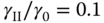 is included.
The conceptual setup for an electric-field-induced half-metallic device is shown in Figure 5.6b. The electric voltage ![]() is applied along the transverse
is applied along the transverse ![]() direction of zigzag nanoribbons; thus, the electric field
direction of zigzag nanoribbons; thus, the electric field ![]() is given by
is given by ![]() . Figure 5.6c shows the energy band structure and corresponding DOS in the presence of an electric field, where the spin degeneracy is lifted. Here, the energy gap for the up-spin starts closing with increasing electric field, while that for the down-spin remains open. In this situation, only up-spins become metallic in the vicinity of
. Figure 5.6c shows the energy band structure and corresponding DOS in the presence of an electric field, where the spin degeneracy is lifted. Here, the energy gap for the up-spin starts closing with increasing electric field, while that for the down-spin remains open. In this situation, only up-spins become metallic in the vicinity of ![]() under the application of transverse electric field, that is, the system becomes half-metallic. The critical electric field strength beyond which the system behaves as half-mettalic, decreases with increase in width of the zigzag nanoribbon [56, 57].
under the application of transverse electric field, that is, the system becomes half-metallic. The critical electric field strength beyond which the system behaves as half-mettalic, decreases with increase in width of the zigzag nanoribbon [56, 57].
5.5 Summary
In this chapter, we have briefly reviewed nanoscale effects on the electronic properties of graphene. The presence of a graphene edge crucially affects the electronic states of nanoscale graphene (nanographene). Two typical types of graphene edges, namely, we al armchair and zigzag edges exhibit completely different electronic properties. Although the presence of an armchair edge tends to preserve the properties of Dirac fermions of graphene, the presence of a zigzag edge is detrimental to Dirac fermions and induces localized edge states at the Fermi energy. Since the presence of edge states produces a non-negligible large peak in the DOS at the Fermi energy of nanographene, the magnetic properties of nanographene are considerably different from those of graphene. We have also seen that the strong Fermi instability of the edge states induces the ferrimagnetic spin polarization even along the zigzag edge. The careful control and theoretical designing of such magnetic states will serve to realize carbon-based spintronic devices.
Since the field of graphene nanotechnology is still growing, we could not include all the important topics in this single chapter. It is also known that the lattice defect or vacancy can also be source of magnetism [58]. The spin–orbit interactions can also be tuned by the hydrogenation to induce the spin-Hall effect [59]. In further, the presence of edge states in graphene nanoribbons becomes a source of a perfectly conducting channel, that is, absence of Anderson localization [50, 60–62]. This peculiar transport properties of nanoribbons will serve to design the ultra-low power consumption electronic devices composed of carbon nanomaterials [41].
The recent rapid progress in graphene research has revealed the unconventional electronic properties of massless Dirac fermion systems. However, we have seen that graphene can exhibit a strong nanoscale edge effect. Such an effect might be the origin of the diverse of physical and chemical properties of aromatic molecules. Further exploration of the physics of nanoscale graphene will be demanded for the realization of carbon-based devices.
References
- 1 Novoselov, K.S., Geim, A.K., Morozov, S.V., Jiang, D., Zhang, Y., Dubonos, S.V., Grigorieva, I.V., and Firsov, A.A. (2004) Electric field effect in atomically thin carbon films. Science, 306 (5296), 666–669.
- 2 Novoselov, K.S., Geim, A.K., Morozov, S.V., Jiang, D., Katsnelson, M.I., Grigorieva, I.V., Dubonos, S.V., and Firsov, A.A. (2005) Two-dimensional gas of massless Dirac fermions in graphene. Nature, 438 (7065), 197–200.
- 3 Zhang, Y.B., Tan, Y.W., Stormer, H.L., and Kim, P. (2005) Experimental observation of the quantum hall effect and Berry's phase in graphene. Nature, 438 (7065), 201–204.
- 4 Geim, A.K. and Novoselov, K.S. (2007) The rise of graphene. Nat. Mater., 6 (3), 183–191.
- 5 Neto, A.H.C., Guinea, F., Peres, N.M.R., Novoselov, K.S., and Geim, A.K. (2009) The electronic properties of graphene. Rev. Mod. Phys., 81 (1), 109–162.
- 6 Ando, T. (2005) Theory of electronic states and transport in carbon nanotubes. J. Phys. Soc. Jpn., 74 (3), 777–817.
- 7 Ando, T. (2008) Physics of graphene - zero-mode anomalies and roles of symmetry. Prog. Theor. Phys. Suppl., 176, 203–226.
- 8 Ando, T. and Nakanishi, T. (1998) Impurity scattering in carbon nanotubes - absence of back scattering. J. Phys. Soc. Jpn., 67 (5), 1704–1713.
- 9 Ando, T., Nakanishi, T., and Saito, R. (1998) Berry's phase and absence of back scattering in carbon nanotubes. J. Phys. Soc. Jpn., 67 (8), 2857–2862.
- 10 Katsnelson, M.I., Novoselov, K.S., and Geim, A.K. (2006) Chiral tunnelling and the Klein paradox in graphene. Nat. Phys., 2 (9), 620–625.
- 11 Bolotin, K.I., Sikes, K.J., Jiang, Z., Klima, M., Fudenberg, G., Hone, J., Kim, P., and Stormer, H.L. (2008) Ultrahigh electron mobility in suspended graphene. Solid State Commun., 146 (9-10), 351–355.
- 12 Balandin, A.A., Ghosh, S., Bao, W.Z., Calizo, I., Teweldebrhan, D., Miao, F., and Lau, C.N. (2008) Superior thermal conductivity of single-layer graphene. Nano Lett., 8 (3), 902–907.
- 13 Fujita, M., Wakabayashi, K., Nakada, K., and Kusakabe, K. (1996) Peculiar localized state at zigzag graphite edge. J. Phys. Soc. Jpn., 65 (7), 1920–1923.
- 14 Nakada, K., Fujita, M., Dresselhaus, G., and Dresselhaus, M.S. (1996) Edge state in graphene ribbons: nanometer size effect and edge shape dependence. Phys. Rev. B, 54 (24), 17 954–17 961.
- 15 Wakabayashi, K., Fujita, M., Ajiki, H., and Sigrist, M. (1999) Electronic and magnetic properties of nanographite ribbons. Phys. Rev. B, 59 (12), 8271–8282.
- 16 Wakabayashi, K., Sigrist, M., and Fujita, M. (1998) Spin wave mode of edge-localized magnetic states in nanographite zigzag ribbons. J. Phys. Soc. Jpn., 67 (6), 2089–2093.
- 17 Wakabayashi, K. (2000) Low-energy physical properties of edge states in nano-graphites. PhD thesis. University of Tsukuba, http://hdl.handle.net/2241/2592 (accessed 8 August 2017).
- 18 Wakabayashi, K. and Harigaya, K. (2003) Magnetic structure of nano-graphite mobius ribbon. J. Phys. Soc. Jpn., 72 (5), 998–1001.
- 19 Fernandez-Rossier, J. and Palacios, J.J. (2007) Magnetism in graphene nanoislands. Phys. Rev. Lett., 99, 177 204.
- 20 Palacios, J.J., Fernandez-Rossier, J., Brey, L., and Fertig, H.A. (2010) Electronic and magnetic structure of graphene nanoribbons. Semicond. Sci. Technol., 25 (3). doi: 10.1088/0268-1242/25/3/033003.
- 21 Hikihara, T., Hu, X., Lin, H.H., and Mou, C.Y. (2003) Ground-state properties of nanographite systems with zigzag edges. Phys. Rev. B, 68 (3), 035 432.
- 22 Son, Y.W., Cohen, M.L., and Louie, S.G. (2006) Energy gaps in graphene nanoribbons. Phys. Rev. Lett., 97 (21), 216 803.
- 23 Kusakabe, K. and Maruyama, M. (2003) Magnetic nanographite. Phys. Rev. B, 67 (9), 092 406.
- 24 Wassmann, T., Seitsonen, A.P., Saitta, A.M., Lazzeri, M., and Mauri, F. (2008) Structure, stability, edge states, and aromaticity of graphene ribbons. Phys. Rev. Lett., 101 (9), 096 402.
- 25 Wakabayashi, K., Okada, S., Tomita, R., Fujimoto, S., and Natsume, Y. (2010) Edge states and flat bands of graphene nanoribbons with edge modification. J. Phys. Soc. Jpn., 79 (3), 034 706.
- 26 Dutta, S., Manna, A.K., and Pati, S.K. (2009) Intrinsic half-metallicity in modified graphene nanoribbons. Phys. Rev. Lett., 102 (9), 096 601.
- 27 Kan, E.J., Li, Z.Y., Yang, J.L., and Hou, J.G. (2008) Half-metallicity in edge-modified zigzag graphene nanoribbons. J. Am. Chem. Soc., 130 (13), 4224–4225.
- 28 Han, M.Y., Özyilmaz, B., Zhang, Y.B., and Kim, P. (2007) Energy band-gap engineering of graphene nanoribbons. Phys. Rev. Lett., 98 (20), 206 805.
- 29 Chen, Z.H., Lin, Y.M., Rooks, M.J., and Avouris, P. (2007) Graphene nano-ribbon electronics. Physica E, 40 (2), 228–232.
- 30 Li, X.L., Wang, X.R., Zhang, L., Lee, S.W., and Dai, H.J. (2008) Chemically derived, ultrasmooth graphene nanoribbon semiconductors. Science, 319 (5867), 1229–1232.
- 31 Kosynkin, D.V., Higginbotham, A.L., Sinitskii, A., Lomeda, J.R., Dimiev, A., Price, B.K., and Tour, J.M. (2009) Longitudinal unzipping of carbon nanotubes to form graphene nanoribbons. Nature, 458 (7240), 872–876.
- 32 Dai, H.J., Jiao, L.Y., Jiao, L.Y., Zhang, L., Wang, X.R., and Diankov, G. (2009) Narrow graphene nanoribbons from carbon nanotubes. Nature, 458 (7240), 877–880.
- 33 Cai, J.M., Ruffieux, P., Jaafar, R., Bieri, M., Braun, T., Blankenburg, S., Muoth, M., Seitsonen, A.P., Saleh, M., Feng, X.L., Mullen, K., and Fasel, R. (2010) Atomically precise bottom-up fabrication of graphene nanoribbons. Nature, 466 (7305), 470–473.
- 34 Liu, J., Li, B.W., Tan, Y.Z., Giannakopoulos, A., Sanchez-Sanchez, C., Beljonne, D., Ruffieux, P., Fasel, R., Feng, X., and Müllen, K. (2015) Toward cove-edged low band gap graphene nanoribbons. J. Am. Chem. Soc., 137 (18), 6097–6103. doi: 10.1021/jacs.5b03017.
- 35 Ruffieux, P., Wang, S., Yang, B., Sánchez-Sánchez, C., Liu, J., Dienel, T., Talirz, L., Shinde, P., Pignedoli, C.A., Passerone, D., Dumslaff, T., Feng, X., Müllen, K., and Fasel, R. (2016) On-surface synthesis of graphene nanoribbons with zigzag edge topology. Nature, 531, 489–492. doi: 10.1038/nature17151.
- 36 Molitor, F., Guttinger, J., Stampfer, C., Graf, D., Ihn, T., and Ensslin, K. (2007) Local gating of a graphene hall bar by graphene side gates. Phys. Rev. B, 76 (24), 245 426.
- 37 Wang, X.R., Ouyang, Y.J., Li, X.L., Wang, H.L., Guo, J., and Dai, H.J. (2008) Room-temperature all-semiconducting sub-10-nm graphene nanoribbon field-effect transistors. Phys. Rev. Lett., 100 (20), 206 803.
- 38 Tapaszto, L., Dobrik, G., Lambin, P., and Biro, L.P. (2008) Tailoring the atomic structure of graphene nanoribbons by scanning tunnelling microscope lithography. Nat. Nanotechnol., 3 (7), 397–401.
- 39 Stampfer, C., Gutttinger, J., Hellmueller, S., Molitor, F., Ensslin, K., and Ihn, T. (2009) Energy gaps in etched graphene nanoribbons. Phys. Rev. Lett., 102 (5), 056 403.
- 40 Miyazaki, H., Odaka, S., Sato, T., Tanaka, S., Goto, H., Kanda, A., Tsukagoshi, K., Ootuka, Y., and Aoyagi, Y. (2008) Coulomb blockade oscillations in narrow corrugated graphite ribbons. Appl. Phys. Express, 1 (2), 024 001.
- 41 Baringhaus, J., Ruan, M., Edler, F., Tejeda, A., Sicot, M., Taleb-IbrahimiAmina, A., Li, A.-P., Jiang, Z., Conrad, E.H., Berger, C., Tegenkamp, C., and de Heer, W.A. (2014) Exceptional ballistic transport in epitaxial graphene nanoribbons. Nature, 506, 349–354. doi: 10.1038/nature12952.
- 42 Sprinkle, M., Ruan, M., Hu, Y., Hankinson, J., Rubio-Roy, M., Zhang, B., Wu, X., Berger, C., and de Heer, W.A. (2010) Scalable templated growth of graphene nanoribbons on SiC. Nat. Nanotechnol., 5 (10), 727–731. doi: 10.1038/nnano.2010.192.
- 43 Wallace, P.R. (1947) The band theory of graphite. Phys. Rev., 71 (9), 622–634.
- 44 Fujita, M., Igami, M., and Nakada, K. (1997) Lattice distortion in nanographite ribbons. J. Phys. Soc. Jpn., 66 (7), 1864–1867.
- 45 Hod, O., Peralta, J.E., and Scuseria, G.E. (2007) Edge effects in finite elongated graphene nanoribbons. Phys. Rev. B, 76 (23), 233 401.
- 46 Miyamoto, Y., Nakada, K., and Fujita, M. (1999) First-principles study of edge states of H-terminated graphitic ribbons. Phys. Rev. B, 59 (15), 9858–9861.
- 47 Kobayashi, Y., Fukui, K., Enoki, T., Kusakabe, K., and Kaburagi, Y. (2005) Observation of zigzag and armchair edges of graphite using scanning tunneling microscopy and spectroscopy. Phys. Rev. B, 71 (19), 193 406.
- 48 Kobayashi, Y., Fukui, K., Enoki, T., and Kusakabe, K. (2006) Edge state on hydrogen-terminated graphite edges investigated by scanning tunneling microscopy. Phys. Rev. B, 73 (12), 125 415.
- 49 Niimi, Y., Matsui, T., Kambara, H., Tagami, K., Tsukada, M., and Fukuyama, H. (2005) Scanning tunneling microscopy and spectroscopy studies of graphite edges. Appl. Surf. Sci., 241 (1-2), 43–48.
- 50 Wakabayashi, K., Takane, Y., Yamamoto, M., and Sigrist, M. (2009) Edge effect on electronic transport properties of graphene nanoribbons and presence of perfectly conducting channel. Carbon, 47 (1), 124–137.
- 51 Wakabayashi, K., Sasaki, K.I., Nakanishi, T., and Enoki, T. (2011) Electronic states of graphene nanoribbons and analytical solutions. Sci. Technol. Adv. Mater., 11, 054 504. doi: 10.1088/1468-6996/11/5/054504.
- 52 Lieb, E.H. (1989) Two theorems on the Hubbard-model. Phys. Rev. Lett., 62 (10), 1201–1204.
- 53 Tao, C., Jiao, L., Yazyev, O.V., Chen, Y.C., Feng, J., Zhang, X., Capaz, R.B., Tour, J.M., Zettl, A., Louie, S.G., Dai, H., and Crommie, M.F. (2011) Spatially resolving edge states of chiral graphene nanoribbons. Nat. Phys., 7, 616–620.
- 54 Magda, G.Z., Jin, X., Hagymasi, I., Vancso, P., Osvath, Z., Nemes-Incze, P., Hwang, C., Biro, L.P., and Tapaszto, L. (2014) Room-temperature magnetic order on zigzag edges of narrow graphene nanoribbons. Nature, 514, 608–611. doi: 10.1038/nature13831.
- 55 Dutta, S. and Wakabayashi, K. (2012) Tuning charge and spin excitations in zigzag edge nanographene ribbons. Sci. Rep., 2, 519. doi: 10.1038/srep00519.
- 56 Son, Y.W., Cohen, M.L., and Louie, S.G. (2006) Half-metallic graphene nanoribbons. Nature, 444 (7117), 347–349.
- 57 Dutta, S. and Pati, S. (2008) Half-metallicity in undoped and boron doped graphene nanoribbons in presence of semilocal exchange-correlation interactions. J. Phys. Chem. B, 112, 1333–1335.
- 58 Yazyev, O. and Helm, L. (2007) Defect-induced magnetism in graphene. Phys. Rev. B, 75, 125 408.
- 59 Balakrishnan, J., Koon, G.K.W., Jaiswal, M., Castro Neto, A.H., and Özyilmaz, B. (2013) Colossal enhancement of spin–orbit coupling in weakly hydrogenated graphene. Nat. Phys., 9, 284–287. doi: 10.1038/nphys2576.
- 60 Wakabayashi, K., Takane, Y., and Sigrist, M. (2007) Perfectly conducting channel and universality crossover in disordered graphene nanoribbons. Phys. Rev. Lett., 99 (3), 036 601.
- 61 Wakabayashi, K., Takane, Y., Yamamoto, M., and Sigrist, M. (2009) Electronic transport properties of graphene nanoribbons. New J. Phys., 11, 095 016.
- 62 Yamamoto, M., Takane, Y., and Wakabayashi, K. (2009) Nearly perfect single-channel conduction in disordered armchair nanoribbons. Phys. Rev. B, 79 (12), 125 421.