
Chapter 13
Optically Active Organic Field-Effect Transistors
Yutaka Wakayama
International Center for Materials Nanoarchitectonics (WPI-MANA), National Institute for Materials Science (NIMS), 1-1 Namiki, Tsukuba, 305-0044, Japan
13.1 Introduction
Electronic devices consisting of organic materials have attracted considerable attention owing to their potential advantages, such as low production cost, large-scale manufacture, solution processability, and mechanical compatibility with plastic substrates. These advantages make it possible to present a new paradigm called “flexible electronics” [1–5]. The organic field-effect transistor (OFET) is a key device in flexible electronics [6–8]. Recently, field-effect carrier mobility has reached 20 cm2 V−1 s−1, which is high enough for practical applications [9]. These achievements have been realized as the result of steady efforts to produce new organic semiconducting materials [10, 11] and to understand the fundamental thin-film growth mechanism [12, 13]. The next stage as regards commercialization is to establish a cost-effective process for large-scale device integration.
Meanwhile, a new trend has recently appeared, where novel functionalities originating in molecules have been incorporated into conventional OFETs. Various functions have been integrated into OFETs including gas sensing, optical switching, memory, spintronics, and light emission [14–20]. These functionalities can be realized owing to the diversity of organic materials. For example, molecular structures can be designed according to the required functions. Among optical functionalities in particular, molecular structures can be tuned to adjust the light-absorbing wavelength. This diversity is an advantage of organic materials.
This chapter reviews optically active OFETs, in which optical functionalities are integrated in conventional transistors. The major merits of such OFETs are the wide wavelength light absorption range and the high responsivity of organic materials to light stimulation. Light signals can be effectively converted into electrical current and amplified in three-terminal transistor structures. These merits enable us to develop various OFETs, such as phototransistors, nonvolatile memories, and optical switching devices. Phototransistors realize the fullest effective photoelectric conversion of the organic materials. Then, the optically generated electrical currents in phototransistors are transient. In contrast, light-induced conformational changes in photochromism are generally permanent. Therefore, photochromism in transistors has other fascinating characteristics, for example, light irradiation permits optical switching with a memory effect and logic circuit patterning, which are impossible to realize in their inorganic counterparts. First, the recent progress in phototransistors is briefly introduced. Then, the focus is on the effective use of photochromic reactions in OFETs used for optical memories, sensors, and switching devices. Finally, a cutting-edge technique, namely, the laser patterning of electrical circuits on thin films of photochromic molecules is described.
13.2 Phototransistors
Optically generated charge carriers (holes/electrons) can be collected in a drain electrode under appropriate source–drain and gate bias voltages. As a result, phototransistors have the potential for use as photoelectric conversion devices, optical sensors, and switching devices. The device has a bottom-gate-type structure, because the channel layers receive light from the top. The three-terminal device architecture of the transistors offers advantages over two-terminal diodes because the transistors can both reduce noise and amplify the electrical signal. Therefore, the organic compounds used for phototransistors require both high optical sensitivity and high carrier mobility.
There are two key parameters for evaluating phototransistor performance. These parameters are photoresponsivity (R = (Ilight − Idark)/L) and photosensitivity (P = (Ilight − Idark)/Idark), where Ilight and Idark represent drain current under light and dark conditions, and L is the intensity of irradiated light. P depends on L, but R depends only on wavelength, and is normalized by L. Thus, the R value is comparable to that of other phototransistors. The assessment criterion for R is 300 A W−1, because this value has been reported for a conventional single-crystal Si phototransistor. To meet this requirement, various device types have been developed. This chapter summarizes recent progress in organic phototransistors by categorizing the dimensionality of organic semiconductors into three types, namely, single crystals (3D), thin films (2D), and nanowires (1D), as illustrated in Figure 13.1.

Figure 13.1 Categorization of phototransistors according to the dimensions of organic semiconductor channels: (a) 3D single crystals, (b) 2D thin films, and (c) 1D nanowires. Each category has its merits and demerits.
13.2.1 Single-Crystal-Based and Nanowire-Based Phototransistors
A major merit of single crystals is that they allow us to examine the fundamental physics of phototransistors [21–24]. Another merit is high carrier mobility, which provides target values. Kim et al. developed a phototransistor based on an anthracene single crystal, whose carrier mobility is in the 0.2–1.6 cm2 V−1 s−1 range [21]. They observed a high R of 1.0–1.1 × 10⁴ A W−1, which is higher than that of a conventional Si phototransistor. On the basis of this excellent R value, they demonstrated a P of 1.4 × 10⁵ under a very low incident light intensity of 1.4 µW cm−2. Moreover, they revealed that an anthracene single crystal has a highly ordered face-to-face arrangement that causes strong intermolecular π–π interactions and promotes the charge transport of photogenerated carriers. This is the main reason for the excellent phototransistor properties that they observed. Jiang et al. reported phototransistors with single crystals of tetracyanoquinodimethane (TCNQ) and tetrathiafulvalene (TTF) [23]. In particular, the TCNQ phototransistor exhibited a fast switching speed of 500 ms. The phenomenon is related to the band gaps and the densely packed molecular arrangement. The low HOMO–LUMO (highest occupied molecular orbital–lowest occupied molecular orbital) gap of TCNQ (2.25 eV), compared with that of TTF (2.76 eV), allows the easy excitation of electrons from HOMO to LUMO. Mukherjee et al. also developed a TCNQ-based phototransistor with a faster switching speed of 10 ms [24]. Here, a polymeric gate dielectric was used, which was effective in reducing carrier trapping sites at the gate insulator/channel layer interface and in improving the switching speed. As described, single crystals have several advantages for phototransistors. However, these crystals are not suitable for practical applications because they are fragile and have poor mass producibility.
Recently, one-dimensional nanowire structures have attracted attention for use with phototransistors. This is because nanowire-based phototransistors have three major advantages. The first is compatibility with flexible devices due to elongated dimension. Second, carrier mobilities are improved due to the single-crystal structure. The third merit is a high surface-to-volume ratio for effective photon-carrier conversion. Hoang et al. synthesized single-crystalline nanowires of π-extended porphyrin derivatives for transistor channels and achieved high performance levels of R = 2.2 × 10⁴ A W−1 and a carrier mobility of 2.90 cm2 V−1 s−1 [25]. This high performance was mainly realized using H-aggregated dimeric porphyrin pairs in the crystalline nanowires, promoting intermolecular π–π interactions, and improving the transport of photogenerated carriers. A similar single-crystal nanowire phototransistor was developed by Yu et al. [26]. The nanowires, which consisted of perylene-based derivatives (BPE-PTCDI), were grown along the a-axis direction with the shortest π-planar distance of 3.4 Å, which is advantageous for effective charge transport along the long axis of the nanowire. The well-ordered molecular alignment exhibited a high R of 1.40 × 10³ A W−1, P of 4.93 × 10³, and a mobility of 1.13 cm2 V−1 s−1 at an optimized wavelength of 532 nm. In this manner, excellent performance has been reported for nanowire transistors [27–30]. However, there is a hurdle to be overcome. Although most of the reported nanowires have been produced via “bottom-up” self-assembly processes, these processes are unsuitable for well-ordered device integration. Thus, the next challenge will be to establish “top-down” nanowire alignment techniques. A promising candidate is a nano-imprinting technique, which allows us to design nanowire arrays [31, 32]. Furthermore, this technique improves the chain alignments of π-conjugated polymers via the nano-confinement effect, which leads to improved carrier transport [33–35].
13.2.2 Thin-Film-Based Phototransistors
Two-dimensional thin films are the most suitable for realistic device applications because of the availability of a wide range of materials and compatibility with practical device structures. However, such advantages have a trade-off relationship with device performance. Cho et al. achieved high values of R (2500–4300 A W−1) and P (4 × 10⁴) using 1,2,4,5-tetra(50-hexyl-[2,20]-bithiophenyl-5-vinyl)-benzene (4(HPBT)-benzene) and 1,2,4,5-tetra(50-hexyl-[2,20]-terthiophenyl-5-vinyl)-benzene (4(HP3T)-benzene) [36]. Although these values are lower than those reported for single crystals, they are the best performance obtained with thin-film organic phototransistors. Pal et al. produced a poly(3-hexylthiophene-2,5-diyl) (P3HT)-based phototransistor using a drop-casting technique, with R = 250 A W−1 and P = 3.8 × 10³ [37]. Other thin-film-based phototransistors have been developed from 2,5-bis-biphenyl-4-yl-thieno[3,2-b]thiophene (BPTT) [38], titanyl phthalocyanine (TiOPc) [39], pentacene [40], and 2,7-bis-(N,N8-diphenylamino)-28,78-bis(biphenyl-4-yl)-9,98-spirobifluorene [41], with R values ranging from 1.3 to 82 A W−1.
For practical applications, other device parameters should be optimized, namely, the operating voltage, threshold voltage, and switching speed. Salinas and Halik inserted a fullerene-attached self-assembled monolayer (C60-SAM) between a gate dielectric Al2O3 layer and a transistor channel layer [42]. The C60 works as an acceptor to reduce the operating voltage. Mok et al. developed a phototransistor with a P3HT-TiO2 composite film [43]. The P3HT absorbs light to produce excitons, and the TiO2 enhances carrier dissociation by trapping electrons to increase the hole density in the P3HT. Such trapped carriers in turn effectively reduce the threshold voltage. Pyo et al. used fluorinated Cu-phthalocyanine (F16CuPc) for the phototransistor channel. Although the R value was very low (about 1.5 mA W−1), they achieved a fast switching speed of less than 10 ms [44, 45]. A key component in this study was poly(4-phenoxy methylstyrene) (P4PMS), which was used as a gate insulating layer. The surface of P4PMS is hydrophobic and has no OH groups that would act as a charge trapping site. These features of P4PMS improved the switching speed. A similar phototransistor with F16CuPc on a polyimide substrate was produced to create a flexible phototransistor [46]. Thus, thin-film-based phototransistors allow us to employ various material engineering and interface engineering approaches to develop device performance.
13.3 Photochromism in OFETs
Some sorts of organic compounds exhibit reversible changes in molecular structures when subjected to alternate UV and visible light exposure. Those compounds are generally referred to as “photochromic molecules,” which have binary, or even ternary, metastable conformations. Typical photochromic reactions can be divided into three types: open-/closed-ring isomerization of diarylethene (DAE), non-ionic/ionic isomerization of spiropyran and cis/trans isomerization of azobenzene (Figure 13.2a). These conformational changes accompany variations in physical properties such as energy level, π-conjugation, color, and polarity. As discussed in the previous section, the photogenerated electrical currents in phototransistors are transient phenomena. In contrast, photo-induced changes in physical properties can remain even after light irradiation has ceased. Therefore, photochromism is particularly applicable to optical memory. Although such potential applications were first proposed a few decades ago, practical devices have not yet been developed. The challenge is to find a way to incorporate photochromism into actual device structures. This section introduces various attempts to incorporate photochromism into OFET device architectures, where the transistor properties can be modulated by a light stimulus in addition to gate and drain bias voltages. These attempts can be divided into three categories: interface engineering, doping in channel/dielectric layers, and the direct use of photochromic layers as channel layers (Figure 13.2b).

Figure 13.2 (a) Reversible changes of photochromic reactions with UV–vis light irradiation: open-/closed-ring isomerization of diarylethene (DAE), ionic/nonionic states of spiropyran, and cis-/trans-conformations of azobenzene. (b) Recent studies of photochromism in organic field-effect transistors at interfaces/surfaces, in channel/dielectric layers, and as the channel layer.
13.3.1 Interface Engineering
A transistor channel, in which drain current flows, is generated by a gate bias voltage in the vicinity of the channel dielectric interface. Thus, the incorporation of photochromic molecules around the channel/dielectric interface is an effective way to induce optical modulation in drain current. Yoshida et al. inserted a DAE thin film at a pentacene channel–dielectric PMMA interface [47]. UV–visible light irradiation induced open-/closed-ring isomerization in the DAE molecules. Carriers in the transistor channel were trapped or released by the corresponding reversible changes in the HOMO–LUMO levels, yielding a light-induced on/off ratio for the drain current (Ion/Ioff) = 5.0.
Troshin and coworkers reported a unique memory device operation, where a spirooxazine (or spiropyran) layer was inserted at a dielectric/fullerene (C60) channel interface [48–50]. A distinctive feature of this device is that the simultaneous application of a programming bias voltage and violet light illumination are needed to cause reversible changes in transistor properties. This is because a bias voltage and light excitation are needed simultaneously to induce a charge transfer between photochromic molecules and C60. The transferred charges cause large shifts in threshold voltage. By tuning the programming voltage, they demonstrated a multilevel nonvolatile memory operation.
Another effective interface engineering approach is to intercalate photochromic molecules at the electrode–channel interface. Then, carrier injections from metal electrodes are modulated by light-induced photochromic reactions. Zhang et al. inserted spiropyran-self-assembling monolayers (SP-SAMs) at the interface of an electrode–pentacene channel [51]. In spiropyran, the magnitude of the dipole moment can be reversibly changed by a photochromic reaction. The photo-induced dipole variation in spiropyran affected the Schottky barrier, thus varying the carrier injection. As a result, they observed an Ion/Ioff of about 1.6. Samorì and coworkers reported a similar attempt [52]. They inserted an azobenzene-SAM at the electrode–N,N′-1H,1H-perfluorobutyl dicyanoperylenecarboxydiimide (PDIF-CN2) interface. And they claimed that the reversible conformational change of azobenzene effectively changed the tunneling barrier between the metal electrode and the transistor channel. They reported an Ion/Ioff of 2.0. A drawback of azobenzene is that cis–trans isomers have different thermal instabilities; a light-produced cis-isomer reverts to a trans-isomer even under dark conditions. DAEs are advantageous in this regard. The same group demonstrated the repeatable optical switching of the drain current under UV–vis alternate light irradiation by using a DAE-SAM layer at an electrode–channel interface [53].
As discussed in the previous section, one-dimensional materials have advantages with respect to a high surface–volume ratio. Azobenzene or spiropyran was attached to the surface of 1D materials such as carbon nanotubes and polymer nanowires [54–56]. In these cases, photochromic molecules are located near the carrier flow, and therefore photochromism has a direct impact on the drain current. Bardavid et al. achieved a high Ion/Ioff of 10 [57].
13.3.2 Doping in Channel/Dielectric Layers
Mixtures of organic semiconductors and photochromic molecules have been used as transistor channels in which the drain current flows through the semiconductors and photochromic molecules work as a dopant to generate additional light-induced modulation in the electrical current. These approaches can simplify the fabrication process compared with the above mentioned interface engineering. For example, as a transistor channel Li et al. used a spiropyran-doped P3HT film [57], which can be formed with a spin-coating technique. They demonstrated repeatable photoswitching, even though the on/off ratio was very small (Ion/Ioff = 1.05). They attributed the observed photoswitching to a light-induced variation in the energy levels. UV irradiation produced an open-ring spiropyran, which involves a reduction in the LUMO level. The reduced LUMO level enhanced electron transfer from the P3HT to the Au electrode. Orgiu et al. proposed a similar approach [58]. The device and molecular structures are illustrated in Figure 13.3, where a bottom-gate and bottom-contact transistor is formed with a DAE-doped P3HT channel layer. UV irradiation produced closed-ring isomers that raised the HOMO level, which can trap holes in the channel layer to reduce the drain current. On the other hand, the open-ring isomer has a lower HOMO level and has no impact on the drain current. As a result, they realized the optical switching of the drain current (Ion/Ioff = 5.0) through the P3HT channel. They have extended this concept to a wide range of materials, namely, small semiconducting molecules [59] and n-type semiconductors [60]. In each study, they adjusted the energy levels and solubility of DAE molecules by changing the substituents on either side of the DAE main framework. Finally, they developed a multilevel nonvolatile memory [61].
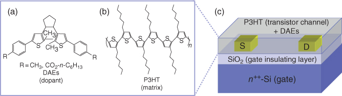
Figure 13.3 (a) DAE molecules are doped as “guests” into (b) a P3HT “host” semiconducting layer in (c) a bottom-gate, bottom-contact OFET.
In these studies, P3HT has generally been used as a host semiconducting layer. Therefore, it is meaningful to discuss the merits and demerits of P3HT for optically active OFETs. P3HT exhibits a photocurrent that should be maximized in the phototransistor because it is the main output signal, as discussed in the previous section. However, the photocurrent should be minimized for photochromism-based transistors because it hinders the drain current, which is the main output signal of these devices. Therefore, the light irradiation conditions, including power, wavelength, and irradiation time, must be carefully optimized in P3HT-based photochromic transistors. Another feature of P3HT is that long alkyl chains are attached along the polythiophene backbone. The alkyl chains allow the solution process to form crystalline thin films. As a result, high carrier mobility can be obtained. However, it should be noted that such a crystalline film has a demerit; the concentration of the dopant has an upper limit due to phase separation. Meanwhile, Ishiguro et al. took advantage of this demerit by intentionally promoting phase separation in a dual-gate transistor [62]. A spiropyran-doped P3HT film (50 wt%) splits a highly segregated bottom layer and a spiropyran-free top layer. These layers work as optically responsive and nonresponsive channels, respectively, allowing multilevel switching. They explained that the ionic polarized state of the open-ring spiropyran created scattering sites that disturbed hole transport. The molecular structures, device configuration, and transistor properties are shown in Figure 13.4.

Figure 13.4 (a) Spiropyran (SP) molecules are doped as “guests” into a P3HT “host” semiconducting layer. (b) Schematic illustrations of a dual-gate transistor, where phase-separated layers (SP-rich bottom layer and SP-free top layer) work as optically inert and active channels, respectively.
To address the issues related to P3HT, Ishiguro's group proposed an alternative host semiconducting polymer, namely, poly[bis(4-phenyl)(2,4,6-trimethylphenyl)amine] (PTAA), as a channel layer [63]. The photocurrent in PTAA is negligible and thus allows limitless light irradiation. The amorphous structure of PTAA allows a high spiropyran doping concentration of up to 70 wt%. By taking advantage of these two factors, they developed a multilevel optical switching device, in which doped and undoped PTAA layers were stacked in a dual-gate transistor configuration [64].
Doping polymeric dielectric layers with photochromic molecules is also an effective way to modify the transistor properties [65, 66]. The spiropyran molecules are dispersed in a PMMA dielectric layer. The photochromic reaction of spiropyran is accompanied by a reversible change in the dipole moment, leading to the photo-induced modification of the dielectric capacitance. An optical switching ratio of Ion/Ioff = 2.0 was reported.
13.3.3 Photochromic Thin Film as Transistor Channel
In general, gate bias voltages generate drain current modulations on the order of 104–106 in OFETs. However, the light-induced Ion/Ioff ratios in the abovementioned studies were only in the 10–80% range and so were much smaller than those of bias-induced current modulations. This is mainly because the photochromic molecules were doped as “guests” into the “host” semiconducting channels. Small amounts of dopant can cause only a marginal modulation in the drain current. In contrast, recent studies have used photochromic molecules directly as transistor channels, aiming at improving Ion/Ioff. Hayakawa et al. used a DAE molecule directly as the transistor channel so that photochromism had a direct impact on the drain current [67]. The device configuration, molecular structures, transfer curves, and optical switching behavior are shown in Figure 13.5. A key point regarding the molecular structure is that the main framework of the DAE was sandwiched by biphenyl substituents. Then, the photochromic reaction between open- and closed-ring DAE is accompanied by a large change in the π-conjugation. And, as a result, a phase transition was induced between the semiconductor and the insulator by alternate UV–vis light irradiation. The DAE film with a closed-ring isomer showed hole transport under certain gate and drain bias voltages; the closed-ring isomer worked as a p-type semiconductor. Meanwhile, the visible light irradiation produced an open-ring isomer, which was an insulator as no electrical current was observed in the transfer curve. With this advantage, they achieved an extremely high on/off ratio of Ion/Ioff = 300. Furthermore, they improved the Ion/Ioff ratio to on the order of 103 by inserting interlayers at the electrode/channel interface and the channel/dielectric layer interface [68]. Based on these achievements, they demonstrated the laser drawing of one-dimensional (1D) channels on an OFET with a photochromic DAE layer. The next section describes such state-of-the-art work on the laser patterning of electrical circuits [69].
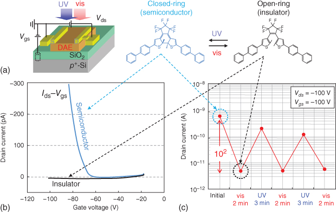
Figure 13.5 (a) Device configuration and molecular structures of DAE. (b) Transfer curves of closed- and open-ring isomers. (c) Optical switching of drain current in a DAE-based transistor.
13.3.4 Laser Patterning of Electric Circuits
An experimental setup for laser patterning and transistor measurement, and molecular structures together with their optical absorption are shown in Figure 13.6. Ne–Cd laser (325.0 nm) and He–Ne laser (632.8 nm) lines are used as the UV and vis lights, respectively. Focused beams 5 µm in diameter are irradiated onto the DAE films through an optical microscope with a 50× objective lens. The DAE transistor is put on a stage whose position can be changed with a stepping motor and an actuator-driven XY-axes stage. The setup makes it possible to perform electrical measurements and spotlight scanning simultaneously. Various kinds of electrical flow path networks, such as multichannel transistors, laser-power-controlled drain currents, branched transistor channels, and optical valves, can be formed with this setup.
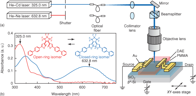
Figure 13.6 (a) Setup for optical patterning and electrical measurement. (b) Absorption spectra of closed- and open-ring DAE isomers.
Figure 13.7 shows the writing and erasing of 1D transistor channels. In Figure 13.7a, the drain current increases with the numbers of channels. Here, a UV spotlight was scanned on the open-ring (insulator) DAE thin film to bridge a pair of electrodes. The scanned area turned to the closed-ring isomer (semiconductor) to work as a transistor channel. Up to three channels were connected with the source–drain electrodes in parallel. Next, thus patterned transistor channels can be erased by scanning the same area with a vis spotlight. The drain current was decreased by erasing connected channels, as shown in Figure 13.7b. In this way, the repeatable writing/erasing of a 1D transistor channel can be easily performed.

Figure 13.7 (a) Writing 1D nanowire channels by UV spotlight scanning. (b) Erasing 1D nanowire channels by vis spotlight scanning. Drain currents are increased (or decreased) with the numbers of the channels.
The drain current is proportional to the ratio of the open-/closed-ring isomers, and the ratio is controllable by controlling the laser power. Therefore, the drain current can be precisely controlled by tuning the irradiated laser power. Figure 13.8 shows stepwise drain currents passing through a 1D transistor channel. Here, UV and vis spotlights with different intensities were scanned sequentially on the DAE film. As shown here, a multilevel drain current can be achieved by controlling the laser power.
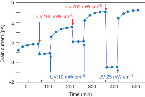
Figure 13.8 Stepwise control of drain current through a 1D channel. Drain current can be tuned by adjusting the power of the scanning UV and vis spotlight.
A key feature of this technique is that various kinds of electrical flow paths can be patterned, for example, zigzag channels, branched channels, and optical valves. An adder circuit can be patterned on the basis of these elements, as shown in Figure 13.9. At the beginning, no current was observed in the initial state (Figure 13.9a). The first channel with a zigzag shape was drawn as shown in Figure 13.9b. Here, a certain UV intensity (UV1) yielded a drain current level “I1.” A second zigzag-shape channel was patterned in a similar manner, where the first and second channels were partially overlapped to form a branched channel (Figure 13.9c). Importantly, the second channel was drawn with higher intensity (UV2 > UV1). Therefore, the drain current through the second channel was higher than that through the first one (I2 > I1). As a result, a total current of “I1 + I2” flowed to the drain electrode. Next, a vis spotlight was irradiated on one space of the first channel to shut off the drain current through this channel (Figure 13.9d). The drain current was reduced from I1 + I2 to I2, and was restored to I1 + I2 by irradiating a UV spotlight on the same position (Figure 13.9e). In this way, the electrical current through the channels can be started and stopped repeatedly. They called this function an “optical valve.” Consequently, the drain current can be controlled at levels of I1, I2, and I1 + I2 as an example of an adder circuit operation.

Figure 13.9 Adder circuit patterning. (a) No current in initial state, (b) zigzag channel patterned by UV1 scanning to yield drain current I1, (c) branched channel patterned by UV2 to yield drain current I2, (d) vis optical valve to close the first channel, and (e) UV optical valve to open the first channel. Multiple drain current levels, I1, I2, and I1 + I2 can be controlled by the position of optical valves.
13.4 Summary and Perspectives
This chapter reviewed recent progress made on optically active OFETs by categorizing them into phototransistors and photochromic transistors. Of these, phototransistors hold promise because some of their parameters surpass those of conventional Si-based phototransistors. Durability needs to be improved. The reported photochromic transistor performance is preliminary and requires further work. However, these devices could open new frontiers for photonic and electronic devices, for example, high-density data storage, optical memory devices, highly sensitive optical sensors, and photon–electron interconnections. In addition, the laser patterning demonstrated in the previous section is achievable owing to the unique property of the DAE molecule, namely, that a semiconductor–insulator phase transition can be induced by UV–vis light irradiation. As a result, networks of the electrical paths can be drawn in an insulator thin film. Although the channel lengths were in the range of several tens of micrometers, the device size can be reduced by utilizing a near-field optical microscope. Another merit of this technique is that it can be used for patterning various logic circuits. Device architectures with multiple electrodes connected by multiple 1D channels can work as an “OR” or “AND” circuit, according to the positions of the optical valves. An example is shown in Figure 13.10. As demonstrated, this technique has the potential to be used to form various optically reconfigurable low-dimensional organic transistor circuits, which are not possible to realize with conventional thin film OFETs.

Figure 13.10 Logic circuit patterning. (a) Initial state, where prepatterned electrodes are connected by a network of 1D channels in an insulator (open-ring) thin film. According to the position of the optical valves, the electrical current paths can be controlled for (b) OR and (c) AND circuits. Here, input and output signals are denoted, I1, I2, and O, respectively.
References
- 1 Friend, R.H., Gymer, R.W., Holmes, A.B., Burroughes, J.H., Marks, R.N., Taliani, C., Bradley, D.D.C., Santos, D.A.D., Brédas, J.-L., Lögdlund, M., and Salaneck, W.R. (1999) Nature, 397, 121.
- 2 Spanggaard, H. and Krebs, F.C. (2004) Sol. Energy Mater. Sol. Cells, 83, 125.
- 3 Lu, G., Usta, H., Risko, C., Wang, L., Facchetti, A., Ratner, M.A., and Marks, T.J. (2008) J. Am. Chem. Soc., 130, 7670.
- 4 Forrest, S.R. (2004) Nature, 428, 911.
- 5 Katz, H.E. (2004) Chem. Mater., 16, 4748.
- 6 Lucas, B., Trigauda, T., and Videlot-Ackermann, C. (2012) Polym. Int., 61, 374.
- 7 Hasegawa, T. and Takeya, J. (2009) Sci. Technol. Adv. Mater., 10, 024314.
- 8 Dimitrakopoulos, C.D. and Malenfant, P.R.L. (2002) Adv. Mater., 14, 99.
- 9 Minemawari, H., Yamada, T., Matsui, H., Tsutsumi, J., Haas, S., Chiba, R., Kumai, R., and Hasegawa, T. (2011) Nature, 475, 364.
- 10 Heimel, G., Salzmann, I., Duhm, S., and Koch, N. (2011) Chem. Mater., 23, 359.
- 11 Yamashita, Y. (2009) Sci. Technol. Adv. Mater., 10, 024313.
- 12 Witte, G. and Wöll, C. (2004) J. Mater. Res., 19, 1889.
- 13 Kowarik, S., Gerlach, A., and Schreiber, F. (2008) J. Phys. Condens. Matter, 20, 184005.
- 14 Guo, Y., Yu, G., and Liu (2010) Adv. Mater., 22, 4427.
- 15 Koopmans, B., Wagemans, W., Bloom, F.L., Bobbert, P.A., Kemerink, M., and Wohlgenannt, M. (2011) Philos. Trans. R. Soc. London, Ser. A, 369, 3602.
- 16 Samuel, I.D.W. and Turnbull, G.A. (2007) Chem. Rev., 107, 1272.
- 17 Sekitani, T., Yokota, T., Zschieschan, U., Klauk, H., Bauer, S., Takeuchi, K., Takamiya, M., Sakurai, T., and Someya, T. (2009) Science, 326, 1516.
- 18 Yang, G., Di, C.-A., Zhang, G., Zhang, J., Xiang, J., Zhang, D., and Zu, D. (2013) Adv. Funct. Mater., 23, 1671.
- 19 Wu, Y., Yin, Z., Xiao, J., Liu, Y., Wei, F., Tan, K.J., Kloc, C., Huang, L., Yan, Q., Hu, F., Zhang, H., and Zhang, Q. (2012) ACS Appl. Mater. Interfaces, 4, 1883.
- 20 Naber, W.J.M., Faez, S., and van der Wiel, W.G. (2007) J. Phys. D: Appl. Phys., 40, R205.
- 21 Kim, K.H., Bae, S.Y., Kim, Y.S., Hur, J.A., Hoang, M.H., Lee, T.W., Cho, M.J., Kim, Y., Kim, M., Jin, J.I., Kim, S.J., Lee, K., Lee, S.J., and Choi, D.H. (2011) Adv. Mater., 23, 3095.
- 22 Mukherjee, B., Sim, K., Shin, T.J., Lee, J., Mukherjee, M., Ree, M., and Pyo, S. (2012) J. Mater. Chem., 22, 3192.
- 23 Jiang, H., Yang, X., Cui, Z., Liu, Y., Li, H., and Hu, W. (2009) Appl. Phys. Lett., 94, 23308.
- 24 Mukherjee, B., Mukherjee, M., Sim, K., and Pyo, S. (2011) J. Mater. Chem., 21, 1931.
- 25 Hoang, M.H., Kim, Y., Kim, M., Kim, K.H., Lee, T.W., Nguyen, D.N., Kim, S.J., Lee, K., Lee, S.J., and Choi, D.H. (2012) Adv. Mater., 24, 5363.
- 26 Yu, H., Bao, Z., and Oh, J.H. (2013) Adv. Funct. Mater., 23, 629.
- 27 Kim, Y.S., Bae, S.Y., Kim, K.H., Lee, T.W., Hur, J.A., Hoang, M.H., Cho, M.J., Kim, S.J., Kim, Y., Kim, M., Lee, K., Lee, S.J., and Choi, D.H. (2011) Chem. Commun., 47, 8907.
- 28 Liu, Y., Dong, H., Jiang, S., Zhao, G., Shi, Q., Tan, J., Jiang, L., Hu, W., and Zhan, X. (2013) Chem. Mater., 25, 2649.
- 29 Wakayama, Y., Hayakawa, R., Chikyow, T., Machida, S., Nakayama, T., Egger, S., de Oteyza, D.G., Dosch, H., and Kobayashi, K. (2008) Nano Lett., 8, 3273.
- 30 Wakayama, Y., Hiroshiba, N., Hayakawa, R., Chikyow, T., and Kobayashi, K. (2012) Jpn. J. Appl. Phys., 51, 06FA01.
- 31 Chen, Y. and Luo, Y. (2009) Adv. Mater., 21, 2040.
- 32 Huang, C., Dong, B., Lu, N., Yang, B., Gao, L., Tian, L., Qi, D., Wu, Q., and Chi, L. (2009) Small, 5, 583.
- 33 Aryal, M., Trivedi, K., and Hu, W. (2009) ACS Nano, 3, 3085.
- 34 Zheng, Z., Yim, K.-H., Saifullah, M.S.M., Welland, M.E., Friend, R.H., Kim, J.-S., and Huck, W.T.S. (2007) Nano Lett., 7, 987.
- 35 Oh, S., Hayakawa, R., Pan, C., Sugiyasu, K., and Wakayama, Y. (2016) J. Appl. Phys., 120, 05501.
- 36 Cho, M.Y., Kim, S.J., Han, Y.D., Park, D.H., Kim, K.H., Choi, D.H., and Joo, J. (2008) Adv. Funct. Mater., 18, 2905.
- 37 Pal, T., Arif, M., and Khondaker, S.I. (2010) Nanotechnology, 21, 325201.
- 38 Noh, Y.-Y., Kim, D.-Y., Yoshida, Y., Yase, K., Jung, B.-J., Lim, E., and Shim, H.-K. (2005) Appl. Phys. Lett., 86, 043501.
- 39 Ji, Z., Shang, L., Lu, C., Wang, L., Guo, J., Wang, H., Li, D., and Liu, M. (2012) IEEE Electron Device Lett., 33, 1619.
- 40 Hu, Y., Dong, G., Liu, C., Wang, L., and Qiu, Y. (2006) Appl. Phys. Lett., 89, 072108.
- 41 Saragi, T.P.I., Pudzich, R., Fuhrmann, T., and Salbeck, J. (2004) Appl. Phys. Lett., 84, 2334.
- 42 Salinas, M. and Halik, M. (2013) Appl. Phys. Lett., 102, 203301.
- 43 Mok, S.M., Yan, F., and Chan, H.L.W. (2008) Appl. Phys. Lett., 93, 023310.
- 44 Mukherjee, B., Mukherjee, M., Choi, Y., and Pyo, S. (2009) J. Phys. Chem. C, 113, 18870.
- 45 Mukherjee, B., Mukherjee, M., Choi, Y., and Pyo, S. (2010) ACS Appl. Mater. Interfaces, 2, 1614.
- 46 Park, J., Mukherjee, B., Cho, H., Kim, S., and Pyo, S. (2011) Synth. Met., 161, 143.
- 47 Yoshida, M., Suemori, K., Uemura, S., Hoshino, S., Takada, N., Kodzasa, T., and Kamata, T. (2010) Jpn. J. Appl. Phys., 49, 04DK09.
- 48 Frolova, L.A., Troshin, P.A., Susarova, D.K., Kulikov, A.V., Sanina, N.A., and Aldoshin, S.M. (2015) Chem. Commun., 51, 6130.
- 49 Frolova, L.A., Rezvanove, A.A., Lukyanov, B.S., Sanina, N.A., Troshin, P.A., and Aldoshin, S.M. (2015) J. Mater. Chem. C, 3, 11675.
- 50 Rezvanove, A.A., Frolava, L.A., and Troshin, P.A. (2016) Mendeleev Commun., 26, 26.
- 51 Zhang, H., Guo, X., Hui, J., Hu, S., Xu, W., and Zhu, D. (2011) Nano Lett., 11, 4939.
- 52 Crivillers, N., Orgiu, E., Reinders, F., Mayor, M., and Samorì, P. (2011) Adv. Mater., 23, 1447.
- 53 Mosciatti, T.G., del Rosso, M., Herder, M., Frisch, J., Koch, N., Hecht, S., Orgiu, E., and Samorì, P. (2016) Adv. Mater., 28, 6606.
- 54 Kim, M., Safron, N.S., Huang, C., Arnold, M.S., and Gopalan, P. (2012) Nano Lett., 12, 182.
- 55 Guo, X., Huang, L., O'Brien, S., Kim, P., and Nuckolls, C. (2005) J. Am. Chem. Soc., 127, 15045.
- 56 Bardavid, Y., Goykhman, I., Nozaki, D., Cuniberti, G., and Yitzchaik, S. (2011) J. Phys. Chem. C, 115, 3123.
- 57 Li, Y., Zhang, H., Qi, C., and Guo, X. (2012) J. Mater. Chem., 22, 4261.
- 58 Orgiu, E., Crivillers, N., Herder, M., Grubert, L., Patzel, M., Frisch, J., Pavlica, E., Duong, D.T., Bratina, G., Salleo, A., Koch, N., Hecht, S., and Samorì, P. (2012) Nat. Chem., 4, 675.
- 59 Gemayel, M.E., Börjesson, K., Herder, M., Duong, D.T., Hutchison, J.A., Ruzié, C., Schweicher, G., Selleo, A., Geerts, Y., Hecht, S., Orgiu, E., and Samorì, P. (2015) Nat. Commun., 6, 6330.
- 60 Börjesson, K., Herder, M., Grubert, L., Duong, D.T., Selleo, A., Hecht, S., Orgiu, E., and Samorì, P. (2015) J. Mater. Chem. C, 3, 4156.
- 61 Leydecker, T., Herder, M., Pavlica, E., Bratina, G., Hecht, S., Orgiu, E., and Samorì, P. (2016) Nat. Nanotechnol., 11, 769.
- 62 Ishiguro, Y., Hayakawa, R., Chikyow, T., and Wakayama, Y. (2014) ACS Appl. Mater. Interfaces, 6, 10415.
- 63 Ishiguro, Y., Hayakawa, R., Chikyow, T., and Wakayama, Y. (2013) J. Mater. Chem. C, 1, 3012.
- 64 Ishiguro, Y., Hayakawa, R., Yasuda, T., Chikyow, T., and Wakayama, Y. (2013) ACS Appl. Mater. Interfaces, 5, 9726.
- 65 Shen, Q., Wang, L., Liu, S., Cao, Y., Gan, L., Guo, X., Steigerwald, M.L., Shuai, Z., Liu, Z., and Nuckolls, C. (2010) Adv. Mater., 22, 3282.
- 66 Lutsyk, P., Janus, K., and Sworakowski, J. (2011) J. Phys. Chem. C, 115, 3106.
- 67 Hayakawa, R., Higashiguchi, K., Matsuda, K., Chikyow, T., and Wakayama, Y. (2013) ACS Appl. Mater. Interfaces, 5, 3625.
- 68 Hayakawa, R., Petit, M., Higashiguchi, K., Matsuda, K., Chikyow, T., and Wakayama, Y. (2015) Org. Electron., 21, 149.
- 69 Tsuruoka, T., Hayakawa, R., Kobashi, K., Higashiguchi, K., Matsuda, K., and Wakayama, Y. (2016) Nano Lett., 16, 7474.