
Chapter 6
Terahertz Broadband Micro-antennas for
Continuous Wave Imaging1
6.1. Introduction
Terahertz waves (THz, 500 GHz to 5,000 GHz, typically) offer a steadily growing range of applications. Traditionally exploited by the radio astronomy and remote sensing communities for the last four decades, they are now expanding over various areas such as atmospheric and environment studies, plasma diagnostics, security, health, transport, etc. [SIE 06].
This growth has led to the introduction into the market of imaging systems based on transient THz waves generated from IR short-pulse sources (femtosecond lasers). However, those systems have begun to exhibit some limitations, in terms of sensitivity, resolution and fast image acquisition, among others.
The two approaches proposed in this chapter are dedicated to the detection of continuous THz waves (CW) using innovative bolometric sensors, to which the incident radiation is coupled by means of wideband micro-antennas, as developed in the NANOTIME project (NANostructures of Oxides for Terahertz IMaging Exploration) [NAN 05].
6.1.1. First approach
This first approach relies basically on the need for high sensitivity heterodyne THz receivers for radio astronomy and remote sensing. The superconducting hot electron bolometer (HEB) — the principle of which was introduced two decades ago [GER 90, PRO 93] — offers a competitive alternative to traditional heterodyne mixing technologies at THz frequencies. Our goal here was to design planar microantennas coupled to HEB mixers implemented with the high critical temperature superconductor YBa2Cu3O6+x (x > 0.5) — also known as YBCO, in the 1 THz to 7 THz range, typically.
Figure 6.1. Left: bolometer structure including a THz planar antenna connected to a superconducting micro-bridge; the high frequency antenna current ITHz creates thermal effects, from which the HEB behavior results within the superconducting material. Right: superconducting resistive transition of an YBCO HEB micro-bridge [PER 06]
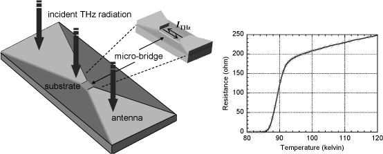
As the YBCO superconductor is highly reflecting for THz waves, the HEB device is connected to a planar antenna to optimize its coupling to the incident electromagnetic radiation (Figure 6.1, left). In addition, the 1 to 7 THz bandwidth we are seeking is much larger than the central frequency, so that introducing ultrawideband (UWB) concepts is required to ensure optimum coupling to the HEB and large radiative efficiency [POW 04]. This requirement is in contrast with the also encountered THz resonant antenna approach [YAS 03]. The impedance matching between the UWB antenna and the HEB will be ensured in view of an operating point of the latter in the middle of the superconducting transition (Figure 6.1, right), i.e. 50 Ω to 150 Ω, typically. The design of a micro-antenna suitable for cryogenic HEBs is discussed in section 6.2.
6.1.2. Second approach
This second approach involves bolometric detectors operating at room temperature, aiming at THz imaging arrays for security and biomedical applications. Here again, the electromagnetic coupling is performed with a planar micro-antenna connected to the bolometer. The latter uses a semiconductor as temperature sensing material, the YBCO semiconducting oxide phase in this case, namely YBa2Cu3O6+x (x < 0.5) [LON 08].
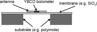
These detectors are based on the classical bolometric principle shown in Figure 6.2 (left), where the electrical resistance is a function of the incident radiation power [KRA 96]. By applying a DC bias current or voltage, the thermal effect gives rise to a voltage or current output signal, respectively, the readout of which can be performed by dedicated electronics (a CMOS ASIC, for instance [MIC 09]). In this case, the sensing YBCO film (300 nm thick, with an area of 50 × 50 μm2, typically) is contacted to planar side contacts etched on a metallic thin film (Figure 6.2a). Due to this restricted area and the low YBCO absorption at THz frequencies, the coupling efficiency to the THz radiation is improved by means of a planar antenna.
Figure 6.2. Left: general principle of a bolometer; from the temperature variation due to the absorbed input radiation results a change of the thermometer resistance. Right: crosssectional view of a metal pad — semiconducting YBCO — metal pad 2 bolometric sensor; high impedance planar structure (a) and lower impedance trilayer structure (b) (typical thicknesses: tmetal = 200 nm; tYBCO = 300 nm)
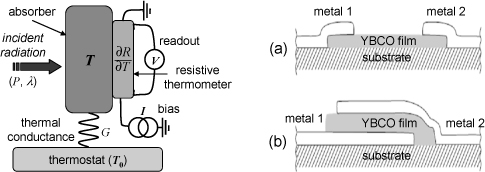
In this context, the challenges for the antenna geometry concern at first a broad bandwidth (1 to 4 THz, typically) and, secondly, the very large resistivity of the YBCO semiconductor (ρ = 300 to 600 Ω.cm). This leads to a resistance value of several MΩ in the case of a meander-shaped planar sensor, a problematic value for coupling to a regular antenna. A partial solution to this difficulty is to switch from the planar structure to a three-layer structure (Figure 6.2b [MOR 07]). As the YBCO thin film is sandwiched between extended metal layers, the impedance of the sensor is significantly reduced down to several kΩ, which leads to seeking an antenna exhibiting an impedance value typically larger than 1 kΩ. The study of wideband micro-antennas suitable to such high impedance uncooled bolometers is discussed in section 6.3.
6.2. UWB THz antennas for superconducting hot electron bolometers
6.2.1. Background on UWB antenna geometry
The antenna function is here to couple the THz radiation propagating in free space to a device with dimensions much smaller than the wavelength. We consider integrated antennas rather than waveguide coupling [KAW 01] for various reasons: lower cost, better accuracy and robustness (at higher frequencies, in particular), and planar geometry well suited to the implementation of arrays [GRO 95].
Antenna characteristics, such as input impedance, radiation pattern or polarization, are invariant under changing the physical dimensions provided similar changes are made on the wavelength or frequency. In other words, performance can be considered as invariant if the electrical dimensions remain unchanged [BAL 05]. Three principles can guide us in designing UWB antennas. Firstly, self-complementarity [MUS 96] depicts the invariance of the antenna geometry when we replace the dielectric regions with metals and vice versa (Figure 6.3a). Secondly, Babinet’s equivalence principle states that the input impedances Z1 and Z2 of two self-complementary antennas are related to the impedance of vacuum η by the relationship [KON 00]:
[6.1] ![]()
In the third place, self-similarity describes the invariance of the electromagnetic behavior when some geometrical shape is repeated at scales that are multiples with respect to each other.
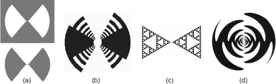
Various wideband micro-antennas exploiting the above-mentioned principles have been considered in detail by Gonzalez et al. for the medium infrared (30 THz) [GON 05]. For our application, the log-periodic [RUM 66], Sierpinski fractal [PUE 96] and sinuous [DUH 87] planar geometries were at first selected due to their widebandwidth and almost constant input impedance, before finally choosing the log-periodic antenna (Figure 6.3b). The Sierpinski (Figure 6.3c) fractal antenna was not chosen because of its multi-band — as opposed to the expected broadband — behavior (several tens of resonances within two octaves). The self-complementary sinuous antenna (Figure 6.3d) was also abandoned because of specific fabrication issues.
Figure 6.3. Some wideband planar antenna geometries (black/dark areas are metallic). From left to right: self-complementary quarter-pie bow-ties (angular concept), self-complementary log-periodic, Sierpinski fractal sieve (self-similar), self-complementary sinuous
6.2.2. The log-periodic planar geometry
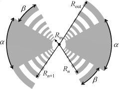
A self-complementary log-periodic planar antenna was developed for a THz mixer to couple the incoming radiation (including both signal and local oscillator) to a superconducting HEB nano-bolometer. The geometrical parameters of the antenna are specified in Figure 6.4. The expected bandwidth for this antenna, consisting of 8 pseudo-dipoles (or arms), spans from 0.9 to 7 THz (330 μm — 43 μm wavelength); the center frequency is 2.5 THz (119 μm line of the water vapor laser [KRE 88]). The key parameter is the scaling τ factor, equal to the ratio between two successive and alternating arm radii. For 8 arms, as selected, we obtain:
[6.2] ![]()
The principle of this antenna has recently been thoroughly analyzed by Scheuring et al. in terms of coupled slot lines [SCH 09]. However, we can approach the main features empirically by considering an arm as active when its length L is equal to one quarter of the effective wavelength λeff. The latter takes into account the dielectric media surrounding the antenna, of effective relative permittivity εeff, namely:
[6.3] ![]()
where λ0 is the wavelength in a vacuum.
The lengths Lmax and Lmin of the outer and inner arms of the antenna are determined from the outer and inner arm radii Rout and Rin, respectively, by using the arm angle β. We deduce the corresponding wavelengths (effective and in vacuum) and the bandwidth edge frequencies fmin and fmax as:
[6.4] ![]()
[6.5] ![]()
[6.6] ![]()
where c is the velocity of light in a vacuum.
Figure 6.4. Self-complementary log-periodic antenna with 8 arms, flare angle α = 60°, arm angle β = 30° (the self-complementarity condition is α + β = 90°. To cover the 0.9 to 7 THz bandwidth, the geometrical parameters are Rin = 7 5 μm and Rout = 58 μm
6.2.3. Input impedance of the planar log-periodic antenna
The frequency behavior of this antenna can be addressed by analyzing a few specific cases. The frequency independence of self-complementary antennas concerns only the limiting case of an infinitely small inner radius and an infinitely large outer radius. In practice, the inner radius is finite and if increased, some impedance oscillations or peaks will be present at high frequencies; similarly, the outer radius will govern the behavior at low frequencies. These intuitive observations were checked in a simple manner by comparing two antennas exhibiting the same scaling factor τ and placed on a substrate of dielectric constant εr = 10, of radii Rin = 2.8 μm and Rout = 22 μm for antenna #1, and radii Rin = 5.2 μm and Rout = 40 μm for antenna #2. These antennas were simulated with CST Microwave Studio® finite elements software [CST 09]; the results are presented in Figure 6.5 (top).
For antennas immersed in free space, we expect the impedance to oscillate around the value of η/2 ≅ 60π ≅ 189 Ω, as given by equation [6.1]. In the present case of an air-dielectric interface, we can use in its place the approximate expression [GRO 95]:
[6.7] ![]()
This expression leads to an impedance value of ≈ 80 Ω for an MgO single crystal substrate (εr = 10 for this material used in our technology). Extra simulations have shown, however, that it was preferable to use the empirical expression εeff ≅ (εr + 5)/2 for an electrically thick MgO substrate.
Figure 6.5. For the log-periodic antenna (see Figure 6.4), real part of the impedance as a function of frequency. Top: influence of the inner radius (larger for antenna #2, see text). Bottom: influence of a ground plane (no ground plane for antenna #4, see text)
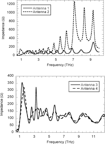
Another issue to address is the effect of a ground plane beneath the substrate. Figure 6.5 (bottom) concerns antennas in free space with dimensions Rin = 1 μm and Rout = 58 μm. The ground plane is located at 50 μm apart from antenna #3, whereas there is no ground plane for antenna #4. Note the pronounced impedance peaks for antenna #3, corresponding to constructive interference at integer multiples of λ/2. This effect is less pronounced at higher frequencies, for which the electrical distance between the antenna and ground plane increases.
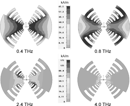
6.2.4. Surface currents of the planar log-periodic antenna
Following the basic considerations presented above (see section 6.2.2), a logperiodic THz antenna has been designed using our empirical approach [TÜR 10a]. The general validity of this approach can be checked by considering the surface current density Js as simulated with CST Microwave Studio®. For this 8-arm antenna, Js is shown in Figure 6.6 at four frequencies. At sub-THz frequency, the behavior is close to that of a quarter-pie bow-tie antenna (see Figure 6.3a) with no arm currents. Close to the bandwidth lower limit (0.9 THz), the 4 outer arms are excited. At the vicinity of the center frequency (2.5 THz) the 5th arms from the center of the structure are active, as expected for the correct operation of the antenna. At high frequencies, several arms resonate close to the center of the structure.
Figure 6.6. Surface currents of the planar 8-arm log-periodic antenna shown in Figure 6.4
6.2.5. Planar log-periodic antenna: design of a large scale microwave model
To allow measurements on large-scale models for experimental flexibility and anechoic chamber availability, the THz bandwidth of the log-periodic antenna (0.9 to 7 THz) was down-shifted to microwaves (namely 2.25 to 17.5 GHz), with a scaling factor close to 400 by wavelength in a vacuum, while keeping the same substrate dielectric constant. More precisely, the center frequency was scaled from 2.5 THz down to 6.1 GHz.
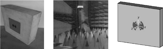
The microwave model substrate was made of ECCOSTOCK® HiK500F [EME 07] material, of thickness 101.6 mm, equivalent to the MgO substrate of thickness 0.25 mm used at THz frequencies (Figure 6.7 left). The antenna itself (of dimensions Rin = 3.0 mm and Rout = 23.2 mm) was etched on 35 μm thick copper laminated on a 1.27 mm thick substrate (Rogers® RT/Duroid 6010LM [ROG 07]). Both ECCOSTOCK® and Rogers® materials exhibit the same dielectric constant as MgO (εr = 10). The two halves of the antenna were excited symmetrically by two semi-rigid RG 405 coaxial cables passing through the substrate and soldered close to the inner arms. The antenna signal was conveyed to the network analyzer by means of a 0°–180° symmetric to asymmetric hybrid broadband coupler (ET Industries, model J-218-180) operating as a balun. The tests were conducted in an anechoic chamber (Figure 6.7 center).
Figure 6.7. Large scale log-periodic planar antenna 2–18 GHz model. Left: copper antenna etched on Rogers® laminate and glued on 30 cm × 30 cm × 10 cm ECCOSTOCK® substrate. Center: anechoic chamber (DRE / SupÉlec). Right: sketch of simulation geometry
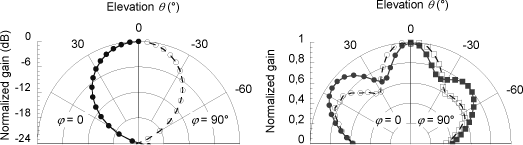
6.2.6. Radiation patterns of the planar log-periodic antenna
The E-plane (xz) and H-plane (yz) (Figure 6.7 right) gain patterns are shown in Figure 6.8 at three frequencies. The measured patterns were compared to those simulated with CST Microwave Studio® (implemented with 40×106 meshes). We can notice an overall satisfactory agreement between measurements and simulations.
Figure 6.8. Radiation gain patterns for the large scale log-periodic antenna model. Measurements (circles) are compared with simulations (thick curves) at 2 GHz / 0.8 THz, 6 GHz / 2.4 THz and 10 GHz / 4 THz
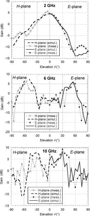
At low frequency (2 GHz / 0.8 THz), the main lobes are of comparable width and the gains at normal incidence exhibit similar values. There are nevertheless secondary lobes around θ = ± 70°, maybe due to experimental system defects such as stray reflections at substrate edges, cable imperfections or small orientation errors.
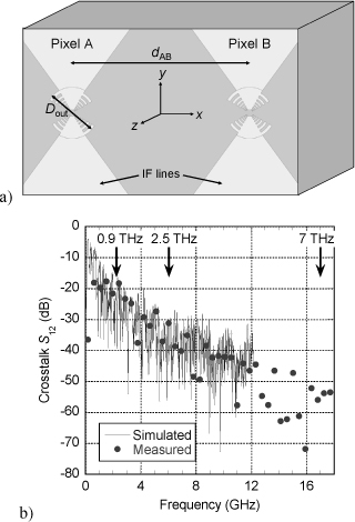
Near the center frequency (6 GHz / 2.4 THz), we observe a decrease of the gain at normal incidence, with a maximum value of about 7 dB close to θ = ± 55° as well as the already mentioned irregularities. We finally observe that the level is reduced to −10 dB at grazing incidence, which is favorable to the reduction of parasitic electromagnetic coupling (crosstalk) between neighbor elements of an imaging array of HEB detectors, as discussed in the next section 6.2.7.
At high frequency (10 GHz / 4 THz), the agreement between measurement and simulation can be considered to be correct up to about |θ| = 45°, with significant discrepancies at large elevation angles. For these frequencies, in fact, the slightest experimental imperfections significantly affect the measurements. Moreover, as the tested structure exhibits a large electrical thickness with respect to the wavelength, the losses due to higher order modes in the substrate significantly affect the overall antenna performance. This drawback can be overcome in a substrate-lens design [RUT 85], the focusing lens dielectric constant being close to that of the substrate.
6.2.7. Electromagnetic coupling between neighboring array elements
With the objective of THz imaging, we have considered the electromagnetic coupling between two log-periodic antennas A and B (i.e. first neighbor pixels of an array) lying at distance dAB along the x-axis in the E-plane (xz) according to the geometry shown in Figure 6.9a. For identical and lossless antennas without polarization mismatch, the far-field coupling coefficient CAB is a function of the gain G(θ = 90°) at 90° elevation angle (in the E-plane) according to Friis transmission equation [FRI 46]:
[6.8] ![]()
A large scale model was built, tested and simulated for two 8-arm log-periodic antennas; the results are shown in Figure 6.9b. As expected, the crosstalk decreases as the frequency increases, with C close to −20 dB at the lower specified frequency (2.25 GHz / 0.9 THz). Although this electromagnetic coupling can be considered to be low, we should also take into account not only the coupling between elements due to thermal diffusion into the substrate [GAU 01], but also the electromagnetic coupling between the intermediate frequency output lines (when the pixels operate as heterodyne mixers) [AUR 10].
Figure 6.9. a) Two neighbor log-periodic antennas (large scale model on a thick substrate) for crosstalk studies. b) For a distance dAB ≈ 3.5 × (antenna diameter Dout), crosstalk S12 = CAB (expression [6.8]) simulated with G(90°) = −6 dB as a function of the frequency
6.2.8. Log-periodic planar antenna implementation with a cryogenic THz detector
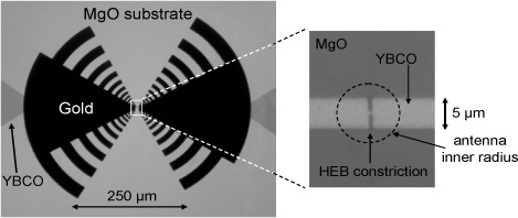
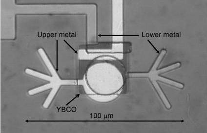
Along with the previous studies, the technological process to produce cryogenic YBCO HEB structures with metal antennas has been developed. The key geometry includes a submicron size constriction e-beam defined on a superconducting microbridge. The whole structure was etched from an ultrathin PBCO / YBCO / PBCO trilayer (PBCO: praseodymium replaces the yttrium in this compound), as shown in Figure 6.10 (right). The gold log-periodic antenna was then fabricated and contacted to the micro-bridge, as shown in Figure 6.10 (left); it consists of a 15-arm device in this case, to cover the 300 GHz to 10 THz ultra-wideband. As already mentioned, the substrate material is 250 μm thick magnesium oxide, (001) oriented MgO single crystal.
Figure 6.10. Optical micrographs of the manufactured log-periodic antenna + HEB microstructure. Left: 15-arm antenna contacting the superconducting YBCO material (outer diameter: 500 μm, inner diameter: 9.5 μm). Right: detail of the central part of the microbridge (overall dimensions: 40 μm×5 μm) etched on an YBCO-based PBCO (4 nm) / YBCO (15 nm) / PBCO (4 nm) ultrathin trilayer; the HEB effect takes place within the central constriction (0.8×0.8 μm2, e-beam lithography) [PER 07]
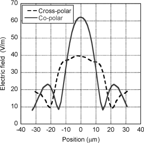
Direct detection CW measurements at 2.5 THz were performed at ≈ 70 K with our first generation test vehicle shown in Figure 6.11 (left). The co-polarization to cross-polarization ratio value was deduced from the measured detected signals in both situations as +4 dB, in line with our simulations (Figure 6.12). The spatial dependence of the cross-polarization detected signal was obtained by moving the THz focused beam longitudinally and transversely, as shown in Figure 6.11 (right). These results are consistent with the characteristics of the antenna on the one hand, and the morphology of the device on the other.
Figure 6.11. Left: THz test vehicle for the superconducting HEB detector with 15-arm logperiodic UWB antenna. The conventional polarization directions are indicated by “Copolar” and “Cross-polar”. Right: measured bolometer response at 2.5 THz (crosspolarization direction); the upper and bottom graphs are for horizontal and vertical translations of the focused THz beam (2 mm diameter), respectively [KRE 07]
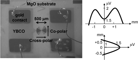
Figure 6.12. For the experimental THz log-periodic antenna, simulated electric field as a function of position from the antenna center, in both polarization orientations [TÜR 10b]
6.3. High-impedance THz antennas for semiconducting bolometers
6.3.1. High-impedance wideband structures
To take into account their implementation in planar multi-pixel bolometer arrays, the antennas must be designed to satisfy various constraints such as size, radiation pattern, polarization bandwidth and impedance. Thus, the size will determine the spatial resolution, gain and response time (through the thermal mass). The radiation pattern must exhibit a strong main lobe in the desired detection direction (perpendicular to the plane of the substrate in the present case) to improve the radiative coupling. In addition, the side lobes must be reduced to avoid detrimental effects of crosstalk between neighboring pixels. In terms of bandwidth, we can consider the various approaches that have been previously described (section 6.2.1), with the high impedance condition added. Such a constraint has also been considered when coupling THz antennas to semiconducting photodetectors or photomixers, either for short-pulse or CW operation [CAS 05, GRE 05].
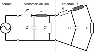
To understand how to adjust the antenna impedance to the required value (see section 6.1.2), let us address the operating principle of an antenna, by considering the general schematic of Figure 6.13. Let us recall that an antenna can be viewed as a loaded degenerate transmission line comprising the capacitive and inductive elements C’ and L’, respectively, as well as the dissipative elements related to the dielectric substrate on the one hand (G’) and metallic parts of finite conductivity (R’) on the other. For low loss materials, the expression of the line impedance can be simplified, namely:
[6.9] 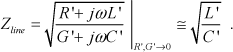
Figure 6.13. General schematic of an antenna coupled to a transmission line
It follows from this expression that the impedance of the line, thus the antenna impedance, can be increased by increasing the inductive component and reducing the capacitive component as well. This can be achieved by choosing structures with narrower metal lines in terms of increased inductance and more separated lines in terms of reduced capacitance. In the following, this approach will be applied to various types of antennas, while keeping in mind the various antenna concepts to achieve wideband operation, as already mentioned previously (see section 6.2.1).
6.3.2. Simulations and measurements: technological approach
The cross-sectional view of a THz bolometric pixel is shown in Figure 6.14. The antenna and YBCO sensor are elaborated on a thin suspended membrane such as silica (SiO2, with relative permittivity εSiO2 = 3.73), with typical thickness tmem = 300 nm, thus avoiding spurious high order modes. The membrane is supported by a substrate such as polyimide (εpoly = 3.5), of typical thickness tpoly = 2 μm. This structure will be our reference for all the antennas considered in the following. Due to the thin membrane and the reduced permittivity of the materials used in this technology, their influence (distortion of the radiation pattern and impedance reduction) has been neglected. All the simulations were performed with the temporal finite element CST Microwave Studio® software. As already mentioned in section 6.2.5, antenna measurements were conveniently performed in an anechoic chamber in the f = 1 to 4 GHz range on large-scale models (size factor ×500 to ×1,000 by wavelength in a vacuum), manufactured on Duroid 6010LM substrate [ROG 07] (εsub = 10.2, tan δsub = 0.0023, thickness tsub = 1.27 mm, with copper laminate of thickness tmet = 35 μm).
Figure 6.14. Structure of a THz bolometric pixel. Both antenna and bolometer are processed on a thin suspended membrane
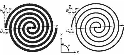
6.3.3. Wideband angular concept: spiral antenna
Two Archimedean spiral (i.e. constant-pitch) antenna structures are shown in Figure 6.15. The antenna on the left is self-complementary (the line width w is equal to the gap s) and therefore exhibits, according to Babinet’s principle, a free-space impedance ZA (Ω) ≅ 60π ≅ 189 Ω (see section 6.2.3). The antenna on the right has the same pitch (w + s), but to increase ZA, the line width has been reduced and the gap accordingly increased.
Figure 6.15. Left: self-complementary spiral THz antenna schematic, with dimensions: w = s = 5 μm and Dmax = 120 μm Right: spiral antenna modified to increase the impedance, with dimensions: w = 2 μm, s = 8 μm and Dmax = 114 μm
The simulated impedances are shown and compared in Figure 6.16a. The curves exhibit the same trends for both structures: while the imaginary part is slightly decreasing, the real part remains practically constant over the whole frequency range.
Figure 6.16. a) Simulated input impedance for both spiral antennas; circles for the self-complementary spiral (Figure 6.15 left), triangles for the non-self-complementary spiral (Figure 6.15 right). b) For two values of the reference impedance Zref, return loss of the non-self-complementary / high-impedance spiral antenna (Figure 6.15 right)
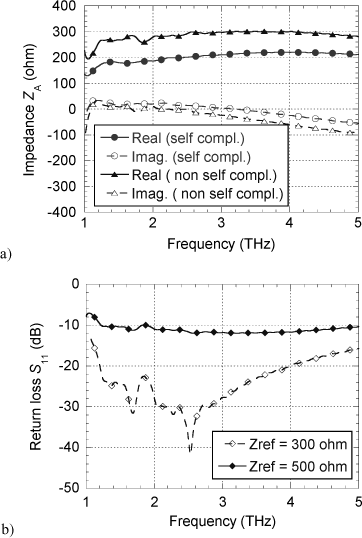
For the second (i.e. non self-complementary) structure, the impedance is increased by about 50% with respect to the first one. Its return loss S11 is shown in Figure 6.16b for two reference impedance values. The impedance of a bolometer suitable for this antenna (i.e. to keep S11 below −10 dB) cannot exceed ~ 500 Ω. The radiation pattern has a main lobe perpendicular to the plane of the substrate, with no side lobes over the whole frequency range. Figure 6.17 shows those diagrams for f = 2 THz and f = 4 THz (left and right, respectively).
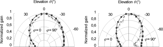
To check the consistency between simulation and experiment, the radiation patterns measured on a microwave large-scale model of the high-impedance antenna (Figure 6.15 right) were compared with simulations. Typical radiation patterns for f = 1 GHz and f = 3.5 GHz are shown in Figure 6.18 (left and right, respectively); they exhibit a satisfactory agreement between experiment and simulation.
Figure 6.17. Simulated radiation pattern of the high-impedance spiral antenna (Figure 6.15 right) at f = 2 THz (left) and f = 4 THz (right)
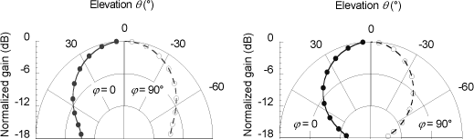
Figure 6.18. Simulated (full symbols) and measured (open symbols) radiation patterns of the high-impedance spiral antenna (Figure 6.15 right large scale model, at f = 1 GHz (left) and f = 3.5 GHz (right)
6.3.4. Modified spiral: square spiral antenna
As a consequence of the circular shape of the spiral antenna, the polarization is also circular. The signals to be detected by a bolometer connected to such an antenna can exhibit any polarization (linear, elliptical or circular). The design of an antenna allowing us to detect radiation in both linear directions at the same time can be sought if considering a square spiral shape. Moreover, square-like shapes may seem a better choice than round shapes for improved packing efficiency in view of 2D arrays. Corner regions can be expected, however, to introduce performance degradation because of discontinuities. Nevertheless, this frequently preferred antenna [GON 05, BRO 08] is briefly considered here.
Figure 6.19. Square spiral THz antenna schematic, with non-self-complementary dimensions: w = 2.5 μm, s = 12.5 μm, Lmin = 2 μm and Lmax = 127.5 μm

The geometrical layout of the modified spiral is shown in Figure 6.19. In order to increase the antenna impedance, the w/s ratio should be decreased with respect to 1 (the self-complementary condition). We have simulated this impedance for w/s = 0.2, and observed a strongly oscillating behavior, with large peaks (over 600 Ω for the real part) in the bandwidth. For this antenna and a reference impedance Zref = 400 Ω, the return loss remains below –10 dB between 1 and 3.4 THz, a noticeable degradation with respect to the circular counterpart.
The simulated radiation pattern exhibits the same features as the circular spiral, with a dominant main lobe (see Figure 6.17). Measurements on a large scale microwave model have shown a satisfactory agreement with simulations, as well.
6.3.5. Log-periodic concept: array of dipoles
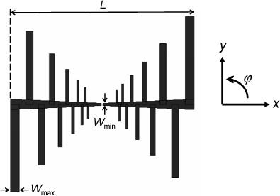
An antenna consisting of an array of coupled dipoles can be proposed as an alternative to obtaining high impedance. The dipole antenna is usually operated as a half wavelength resonator; its impedance is low because the resonator current exhibits a maximum at the central feed point. This current becomes vanishingly small, however, for a full wavelength dipole resonator, from which results — in theory — infinite input impedance. Because of the narrow bandwidth of such a resonator, the concept has been applied to a log-periodic array structure, so as to cover a large bandwidth. The final geometry is shown in Figure 6.20.
Figure 6.20. Sketch of the THz log-periodic array of dipoles, of dimensions: Wmin = 2 μm, Wmax = 7.2 μm and L = 151 μm. The scaling factor τ = 1.2 for this antenna
The overall performance is in practice limited by manufacturing parameters such as the line width, with a maximum average impedance of ≈ 300 Ω in our case, as shown by the ZA(f) graph in Figure 6.21 (left). The return loss S11 remains below −10 dB for a reference impedance Zref = 400 Ω, as shown in Figure 6.21 (right).
The results concerning the radiation pattern suggest the same conclusions as for the spiral antenna, as shown in the example in Figure 6.22 (left). Measurements on a large-scale microwave model show a good correlation with the simulations, as illustrated by the example in Figure 6.22 (right).
Figure 6.21. Log-periodic array of dipoles (Figure 6.20). Left: simulated input impedance. Right: return loss for two values of the reference impedance Zref
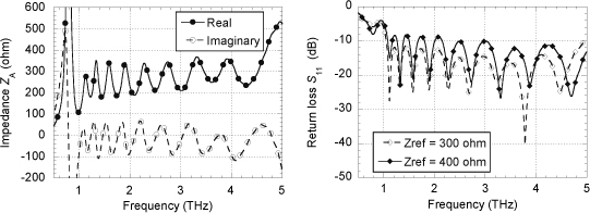
Figure 6.22. Log-periodic array of dipoles (Figure 6.20): radiation patterns. Left: simulated at f = 2 THz (squares) and f = 4 THz (circles). Right: simulated (full symbols) and measured (open symbols) of the large-scale microwave antenna model at f = 3.5 GHz
6.3.6. New concept: multi-tail dipole antenna with ground plane
We have just checked in the previous examples (Sections 6.3.3 to 6.3.5), the effectiveness of the transmission line approach to increase the input impedance of THz micro-antennas. The impedance could be increased by about 50% as compared with regular self-complementary geometries, while keeping a broadband criterion (2 octaves at least). However, our reference impedance value — at least 1 kΩ — could not be reached. We therefore turned our attention to a technique implementing a mutual coupling effect so as to obtain an additional factor of impedance increase [SYD 05]. In this approach, a planar dipole antenna was placed parallel at some distance d from a metal ground plane. The coupling to the ground plane has, however, the effect of creating narrow impedance peaks. Consequently, to expand the frequency band of the device, slightly different extension lengths have been added to obtain the “multi-tail” or “chicken leg” antenna shown in Figure 6.23.
Figure 6.23. Sketch of the multi-tail THz antenna with ground plane geometry, of dimensions: W = 5 μm, Ltail = 37 μm, L = 118 μm and d = 10 μm (air gap) [SCH 10]
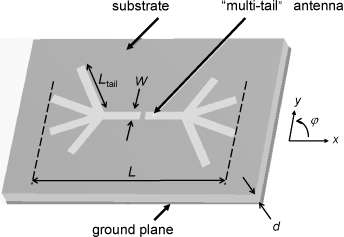
Figure 6.24. Multi-tail antenna with ground plane (Figure 6.23). Left: simulated input impedance as a function of frequency. Right: return loss for a reference impedance of 2 kΩ
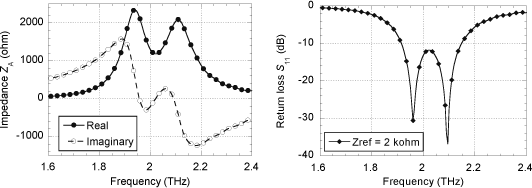
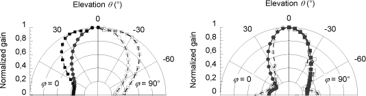
The simulated impedance of this antenna (Figure 6.24 (left)), exhibits a ≈ 15% bandwidth (according to the Re(ZA) > 1 kΩ criterion) around the center frequency. For a reference impedance equal to 2 kΩ, the bandwidth is ≈ 10% for a return loss criterion S11 < −10 dB, as shown in Figure 6.24 (right). Similarly to the antennas described above, the radiation pattern exhibits a main lobe within the bandwidth; an example is shown in Figure 6.25 (left) at f = 2.1 THz.
Figure 6.25. Multi-tail dipole antenna with ground plane (Figure 6.23): radiation patterns. Left: simulated at f = 2.1 THz. Right: simulated (full symbols) and measured (open symbols) for the large scale model at f = 2.1 GHz
In order to test a large-scale model in a microwave anechoic chamber, the antenna structure was fixed on an ECCOSTOCK® substrate (εsub = 10, tan δsub < 0.002) [EME 07] of thickness tsub = 6.35 mm and wsub = lsub = 305 mm overall dimensions. Unlike the thin membrane structure shown in Figure 6.14, this massive and thick substrate can propagate many modes. As a result, the radiation pattern exhibits side lobes (Figure 6.25 (right)), confirming the necessity of using a thin substrate in the final THz structure (such an approach also offers the advantage of a more sensitive bolometer, due to the reduced thermal conductance [JAG 09]).
Simulations and measurements are in satisfactory agreement with respect to the main lobe; the side lobe level is significantly higher for the simulation, however.
6.3.7. THz multi-tail dipole: implementation example
The development of the technological process for fabricating the semiconducting YBCO bolometer and its associated micro-antenna has been tackled. The metal/YBCO/metal trilayer was deposited sequentially on a silicon substrate coated with a thin layer of thermal oxide. The sticking of gold onto the substrate was ensured by a titanium thin film. Electrical and near infrared optical characterizations were performed to study the bolometric response [JAG 10]. The antenna was fabricated according to the multi-tail geometry (section 6.3.6), as shown in Figure 6.26.
Figure 6.26. Multi-tail dipole antenna (see Figure 6.23) coupled to a metal / YBCO / metal trilayer bolometric structure (see Figure 6.2b). Each metal level includes an antenna pad and a biasing + readout contact. The sensing YBCO layer area is 35 μm × 35 μm [JAG 10]
6.4. Conclusion
Facing a fast growing demand on THz systems generated by the diversity of applications either already implemented or potential, we have considered two types of bolometric sensors coupled to the incident radiation by planar micro-antennas.
Considering at first an ultra-wideband antenna coupled to a superconducting hot electron bolometer (HEB), we selected — among several types — the self-complementary log-periodic geometry. The substrate on which the HEB structure is fabricated should be specifically tailored to the high-Tc superconductor used (YBCO), MgO single crystal in this case. Due to the large substrate thickness (250 μm) and its high permittivity (εr = 10), many higher order modes can develop. It therefore follows that the coupling of the antenna to free space is restricted, despite the use of a reflecting ground plane at the substrate backplane. The structure was simulated with finite elements software and the appropriateness of the simulation parameters was checked with the help of a large scale microwave model, which was tested in an anechoic chamber, showing a satisfactory agreement between simulation and experiment.
To improve HEB coupling to free space, it will be necessary to use a focusing lens made from a material with permittivity close to that of the substrate and transparent to THz waves: MgO is obvious, but low-loss semi-insulating silicon (with adequate anti-reflection coating) is usually preferred. The presence of a ground plane and the use of a focusing lens are approaches compatible with THz mixer-block technology. Further development concerns the design and implementation of linear arrays of HEB + antenna pixels, a key point being to satisfy the compromise between spatial resolution and crosstalk interference between pixels. THz direct detection experiments with a first generation test vehicle (cooled down to ≈ 70 K) have also confirmed the reduced dependence of the logperiodic antenna sensitivity to the polarization direction of the incident radiation, an important feature for some applications in astronomy or atmospheric physics.
Secondly, we have suggested several wideband antenna design approaches to address the problem of efficient antenna coupling to high impedance (i.e. around 1 kΩ) semiconducting YBCO bolometers operating at room temperature. Starting at first from self-complementary spiral antennas, we have shown that suitable changes of the geometric parameters lead to an increase in the impedance by about 50% over a 2-octave bandwidth for the circular spiral, but with less improvement for the square spiral. We then proposed a log-periodic array of full-wave dipoles, for which very high impedance is in principle accessible because the feeding current is theoretically vanishingly zero at the dipole center. Geometrical and technological constraints are limiting factors, however, with a maximum impedance value of 300 Ω to 500 Ω, over a 3-octave bandwidth.
We finally proposed a novel structure consisting of a “multi-tail” or “chicken leg” dipole antenna with a reflecting ground plane that allowed us to design a 2 kΩ impedance antenna, typically, but exhibiting a bandwidth reduced to about 10% as a counterpart. Large-scale microwave models were also fabricated and measured in an anechoic chamber to consolidate the simulation results: a satisfactory agreement was observed. The processing technology of bolometer + antenna pixels is being developed to produce 2D arrays for active THz imaging.
6.5. Acknowledgments
This research project has been supported by a Marie Curie Early Stage Research Training Fellowship of the European Community’s Sixth Framework Programme under contract number MEST-CT-2005-020692. We wish to thank Dr Nicolas Ribière-Tharaud for his assistance in setting up anechoic chamber experiments at the Department of Research in Electromagnetism (DRE) in SUPELEC. We would also like to express our gratitude to Dr. Luc Duchesne, of the company SATIMO (Courtabœuf, France) for many discussions and advice on microwave simulation and measurement.
6.6. Bibliography
[AUR 10] AURINO M., KREISLER A.-J., TÜRER I., MARTINEZ A., GENSBITTEL A., DÉGARDIN A.-F., “YBCO hot electron bolometers dedicated to THz detection and imaging: embedding issues”, Journal of Physics: Conference Series, vol. 234, p. 042002, 2010.
[BAL 05] BALANIS C.-A., Antenna Theory: Analysis and Design, Third edition, John Wiley & Sons, New York, 2005.
[BRO 08] BROWN E.-R., “Terahertz Sources — Laser advances drive THz photoconductive source technology”, Laser Focus World, vol. 44, no. 6, 2008.
[CAS 05] CASTRO-CAMUS E., LLOYD-HUGHES J., JOHNSTON M.-B., FRASER M.-D., TAN H. H., JAGADISH C., “Polarization-sensitive terahertz detection by multicontact photoconductive receivers”, Appl. Phys. Lett., vol. 86, pp. 254102–254104, 2005.
[CST 09] http://www.cst.com
[DUH 87] DUHAMEL R.-H., Dual polarized sinuous antennas, U.S. Patent 4,658,262, April 14, 1987.
[EME 07] EMERSON & CUMING, Microwave Products, http://www.eccosorb.com
[FRI 46] FRIIS H.-T., “A note on a simple transmission formula”, Proc. IRE, vol. 34, pp. 254-256, 1946.
[GAU 01] GAUGUE A., TESTÉ PH., DELERUE J., GENSBITTEL A., DE LUCA A., KREISLER A., VOISIN F., KLISNICK G., REDON M., “YBaCuO Mid-Infrared bolometer: substrate influence on inter-pixel crosstalk”, IEEE Trans. Applied Supercond., vol. 11, no. 1, pp. 766–769, 2001.
[GER 90] GERSHENZON E.-M., GOL’TSMAN G.-N., GOGDIZE I.-G., GUSEV Y.-P., ELANT’EV A.-I., KARASIK B.-S., SEMENOV A.-D., “Millimeter and submillimeter range mixer based on electron heating of superconducting films in the resistive state”, Sov. Phys. Superconductivity, vol. 3, no. 10, pp. 1582–1597, 1990.
[GON 05] GONZALEZ F.-J., BOREMAN G.-D., “Comparison of dipole, bow-tie, spiral and logperiodic IR antennas”, Infrared Physics and Technology, vol. 46, pp. 418–428, 2005.
[GRE 05] GREGORY I.-S., BAKER C., TRIBE W.-R., BRADLEY I.-V., EVANS M.-J., LINFIELD E. H., DAVIES A.-G., MISSOUS M., “Optimization of photomixers and antennas for continuous-wave terahertz emission”, IEEE Journal of Quantum Electronics, vol. 41, no. 5, pp. 717–728, 2005.
[GRO 95] GROSSMAN E.-N., “Lithographic antennas for submillimeter and infrared frequencies”, IEEE International Symposium on Electromagnetic Compatibility, Atlanta, USA, August 1995, vol. 14–18, pp. 102–107.
[JAG 09] JAGTAP V.-S., SCHEURING A., LONGHIN M., KREISLER A.-J., DÉGARDIN A.-F., “From superconducting to semiconducting YBCO thin film bolometers: sensitivity and crosstalk investigations for future THz imagers”, IEEE Trans. Appl. Supercond., vol. 19, no. 3, pp. 287–292, 2009.
[JAG 10] JAGTAP V.-S., LONGHIN M., KULSRESHATH M.-K., KREISLER A.-J., DEGARDIN A.-F., “Migrating from superconducting to semiconducting YBCO thin film bolometers as future far-infrared imaging pixels”, Proc. of SPIE, vol. 7671, pp. 76710X–1/9, 2010.
[KAW 01] KAWAMURA J., TONG C.-Y.-E., BLUNDELL R., PAPA D.-C., HUNTER T.-R., PATT F., GOL’TSMAN G., GERSHENZON E., “Terahertz-frequency waveguide NbN hot-electron bolometer mixer”, IEEE Trans. Appl. Supercond., vol. 11, no. 1, pp. 952–954, 2001.
[KON 00] KONG J.-A., Electromagnetic Wave Theory, EMW Publishing, Cambridge, 2000.
[KRA 96] KRAUS H., “Superconducting bolometers and calorimeters”, Supercond. Sci. Technol., vol. 9, pp. 827–842, 1996.
[KRE 88] KREISLER A., SENTZ A., “The water-vapour discharge laser: a convenient tool for CW studies in the far-infrared”, 3rd Conference on Microwaves and Optoelectronics (MIOP), paper 7c4, Wiesbaden, Germany, March 1988.
[KRE 07] KREISLER A.-J., DÉGARDIN A.-F., AURINO M., PÉROZ CH., VILLÉGIER J.-C., BEAUDIN G., DELORME Y., REDON M., SENTZ A., “New trend in terahertz detection: high Tc superconducting hot electron bolometer technology may exhibit advantages vs. low Tc devices”, Proc. IEEE International Microwave Symposium, pp. 345–348., Honolulu, USA, July 2007.
[LON 08] LONGHIN M., KREISLER A.-J., DÉGARDIN A.-F., “Semiconducting YBCO Thin Films for Uncooled Terahertz Imagers”, Materials Science Forum, vol. 587–588, pp. 273–277, 2008.
[MIC 09] MICHAL V., KLISNICK G., SOU G., REDON M., KREISLER A.-J., DÉGARDIN A.-F., “Fixed-gain CMOS differential amplifiers with no external feedback for a wide temperature range”, Cryogenics, vol. 49, p. 615–619, 2009.
[MOR 07] MORENO M., KOSAREV A., TORRES A., AMBROSIO R., “Fabrication and performance comparison of planar and sandwich structures of micro-bolometers with Ge thermo-sensing layer”, Thin Solid Films, vol. 515, pp. 7607–7610, 2007.
[MUS 96] MUSHIHAKE Y., Self-complementary Antennas, Springer-Verlag, Berlin, 1996.
[NAN 05] http://nanotime.lgep.supelec.fr.
[PER 06] PÉROZ CH., VILLÉGIER J.-C., DÉGARDIN A.-F., GUILLET B., KREISLER A.-J., “High critical current densities observed in PrBa2Cu3O7−δ / YBa2Cu3O7−δ / PrBa2Cu3O7−δ ultrathin film constrictions”, Appl. Phys. Lett., vol. 89, pp. 142502–142504, 2006.
[PER 07] PÉROZ CH., DÉGARDIN A.-F., VILLÉGIER J.-C., KREISLER A.-J., “Fabrication and characterization of ultrathin PBCO/YBCO/PBCO constrictions for hot electron bolometer THz mixing applications”, IEEE Trans. Appl. Supercond., vol. 17–2, no. 2, pp. 637–640, 2007.
[POW 04] POWELL JOHNNA, Antenna Design for Ultra Wideband Radio, Master Thesis, Massachusetts Institute of Technology, USA, 2004.
[PRO 93] PROBER D.-E., “Superconducting terahertz mixer using a transition-edge microbolometer”, Appl. Phys. Lett., vol. 62, pp. 2119–2121, 1993.
[PUE 96] PUENTE C., ROMEU J., POUS R., CARDAMA A., “Fractal multiband antenna based on the Sierpinski gasket”, IEE Electronics Letters, vol. 32, no.1, pp. 1–2, 1996.
[ROG 07] www.rogerscorporation.com.
[RUM 66] RUMSEY V.-H., Frequency-Independent Antennas, Academic Press, New York, 1966
[RUT 85] RUTLEDGE D., “Substrate-lens coupled antennas for millimeter and submillimeter waves”, IEEE Antennas and Propagation Society Newsletter, August 1985, pp. 5–8.
[SCH 09] SCHEURING A., WUENSCH S., SIEGEL M., “A novel analytical model of resonance effects of log-periodic planar antennas”, IEEE Trans. Ant. Propag., vol. 57, pp. 3482–3488, 2009.
[SCH 10] SCHEURING A., TÜRER I., RIBIèRE-THARAUD N., DÉGARDIN A.-F., KREISLER A.-J., “Modeling of broadband antennas for room temperature terahertz detectors”, in F. SABATH et al. (eds), Ultra Wideband, Short-pulse Electromagnetics, vol. 9, pp. 277–286, 2010.
[SIE 06] SIEGEL P.-H., DE MAAGT P., ZAGHLOUL A.-I., “Antennas for terahertz applications”, IEEE Antennas and Propagation Society International Symposium, Paper 354–1, pp. 2383–2386, Albuquerque, New Mexico, USA, July 2006.
[SYD 05] SYDLO C., SIGMUND J., HARTNAGEL H.-L., MENDIS R., FEIGINOV M., MEISSNER P., “Planar Terahertz Antenna Optimisation”, Proc. IEEE/ACES International Conference on Wireless Communications and Applied Computational Electromagnetics, pp. 878–882, Honolulu, Hawaii, USA, April 2005.
[TÜR 10a] TÜRER I., GAZTELU X., RIBIÈRE-THARAUD N., DÉGARDIN A.-F., KREISLER A.-J., “Modeling broadband antennas for hot electron bolometers at terahertz frequencies”, in F. SABATH et al. (eds), Ultra Wideband, Short-pulse Electromagnetics, vol. 9, Springer, 2010, pp. 179–188.
[TÜR 10b] TÜRER I., Modelling investigations for terahertz cooled and uncooled imaging arrays, PhD Thesis, UPMC University of Paris 6, France, 2010.
1 Chapter written by Alain KREISLER, Ibrahim TÜRER, Xabier GAZTELU, Alexander SCHEURING and Annick DÉGARDIN.